Spatial-temporal redistribution of point defects in three-layer stressed
nanoheterosystems within the framework of self-assembled deformation-diffusion model
(Received November 20, 2014, in final form February 10, 2015)
Abstract
The model of spatial-temporal distribution of point defects in a three-layer stressed nanoheterosystem GaAs/InxGa1-xAs/GaAs considering the self-assembled deformation-diffusion interaction is constructed. Within the framework of this model, the profile of spatial-temporal distribution of vacancies (interstitial atoms) in the stressed nanoheterosystem GaAs/InxGa1-xAs/GaAs is calculated. It is shown that in the case of a stationary state (), the concentration of vacancies in the inhomogeneously compressed interlayer is smaller relative to the initial average value by 16%.
Побудовано модель просторово-часового розподiлу точкових дефектiв у тришаровiй напруженiй наногетеросистемi GaAs/InxGa1-xAs/GaAs з врахуванням самоузгодженої деформацiйно-дифузiйної взаємодiї. У межах цiєї моделi розраховано профiль просторово-часового розподiлу вакансiй (мiжвузлових атомiв) у напруженiй наногетеросистемi GaAs/InxGa1-xAs/GaAs та показано, що у випадку встановлення стацiонарного стану (), концентрацiя вакансiй в неоднорiдно стиснутому внутрiшньому шарi є меншою вiдносно вихiдного середнього значення на 16%.
Intensive development of nanotechnologies has provided an opportunity to create nanoelectronic devices on the basis of stressed nanoheterosystems GaAs/InxGa1-xAs/GaAs (ZnTe/Zn1-xCdxTe/ZnTe). The active region of such structures are layers InxGa1-xAs, Zn1-xCdxTe, in which the electron-hole gas is localized being bounded on two sides of the potential barriers GaAs (ZnTe).
It is known that optical and electric properties of such devices depend significantly on both the lattice deformation of the contacting systems and the spatial distribution of point defects.
Such defects can penetrate from the surface or arise in the process of epitaxial growth. Besides, diffusion processes play an important role in the technology of fabricating optoelectronic devices. They are related with the redistribution of impurities in a semiconductor structure caused by both the ordinary gradient concentration of defects and the gradient of deformation tensor.
The interaction of defects with the deformation field, created by both the mismatch of the crystal lattice of the contacting materials and the point defects, causes a spatial redistribution of the latter. It can lead both to accumulation and to a decrease of the number of defects in the active region (InxGa1-xAs, Zn1-xCdxTe) of the operating element depending on the character of the deformation created both by the mismatch between parameters of contacting crystal lattices ( () for GaAs/InxGa1-xAs/GaAs (ZnTe/Zn1-xCdxTe/ZnTe), respectively [1, 2]), and by the action of defects. In particular, it is known that the gallium arsenide grown using the method of the molecular-beam epitaxy at low temperature contains an excess of arsenic [3, 4]. Introduction of excessive arsenic causes a tetragonal distortion of the lattice material GaAs and the generation of point defects in it: interstitial atoms (As), vacancies (Ga) and antistructural defects (As), which, in turn, leads to their spatial redistribution. The lattice deformation and concentration of point defects generated under the action of the gradient of deformation tensor depend on the mismatch between the lattice parameters of contacting layers of heterostructure, the temperature of growth, molecular fluxes Ga and As, concentration and chemical nature of the doped impurities.
The strain caused by the mismatch between the lattice of the epitaxial layer and the substrate can be elastic when the thickness of the layer does not exceed a defined critical value [5]. Otherwise, mismatch dislocations are formed accompanied by a sharp worsening of both the optical and the electric characteristics of devices. However, in the layers InxGa1-xAs with the mismatch less than critical there is a significant decline of the mobility and the intensity of photoluminescence at certain terms [5], which is related to the increased number of point defects and a corresponding increase of the diffusion barrier to the atoms of the third group.
In experimental work [6], it is shown that in a heterostructure GaAs/InxGa1-xAs, the stressed quantum-size heterolayers hamper the diffusion of hydrogen and defects into the bulk of the material which leads to a substantial difference of their spatial distribution in a heterostructure and homogeneous layers. Theoretical research of the stationary distribution of defects within the framework of the self-assembled deformation-diffusion model has been considered in the work [7].
Therefore, in order to create devices with prescribed physical properties, it is necessary to construct a spatial-temporal deformation-diffusion model that describes the self-assembled deformation-diffusion processes in stressed nanoheterostructures having their own point defects and impurities.
The aim of this work is to construct a spatial-temporal deformation-diffusion model and calculate the spatial-temporal profile distribution of point defects (interstitial atoms and vacancies) in three-layer stressed nanoheterosystems GaAs/InxGa1-xAs/GaAs (ZnTe/Zn1-xCdxTe/ZnTe).
2 The model of spatial-temporal redistribution of defects
in a three-layer stressed nanoheterosystem
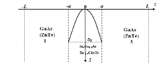
Let us consider stressed nanoheterosystems GaAs/InxGa1-xAs/GaAs (ZnTe/Zn1-xCdxTe/ZnTe) having interlayers InAs (CdTe) of the thickness , that include three layers (figure 1), where , , are the initial average defect concentrations, respectively, and , , are diffusion coefficients. Suppose that the external layers GaAs (ZnTe) are of the thickness that considerably exceeds the width of the interlayer of the heterostructure (), so deformation of these layers can be neglected [, ].
Figure 1: The model of stressed nanoheterostructures
GaAs/InxGa1-xAs/GaAs (ZnTe/Zn1-xCdxTe/ZnTe).
The mechanical deformation that occurs due to the mismatch between the lattice parameters of contacting materials of a heterosystem is approximated by the function [7]:
(1)
where is the relative change of the elementary cell volume of the grown layer on heteroboundaries ; , , where corresponds to the layers GaAs (ZnTe), corresponds to the interlayers InxGa1-xAs (Zn1-xCdxTe); are the crystal lattice parameters of the contacting materials GaAs (ZnTe) and InAs (CdTe) of the heterostructure, respectively; and are the elastic constants of the material InxGa1-xAs (Zn1-xCdxTe).
Epitaxial growth on a substrate with the mismatch between the lattice parameters takes place simultaneously with the diffusion process, which is caused by both the concentration gradient of point defects [] and the gradient parameter of deformation []. The latter induces an additional diffusion flux of defects, which is opposite to the ordinary gradient concentration flux of defects. Therefore, in the basis of this model it is necessary to put a self-assembled system of non-stationary equations for the parameter deformation and concentration of impurities in a stressed heterosystem, the redistribution of which is performed similarly to an ordinary diffusion flux,
thus, by the deformation component of the flux
where is the mechanical deformation potential, is the module of uniform compression of the -th material, is the variation of elementary cell volume at the presence of a defect in the -th layer.
Let the point defects be distributed with the initial average concentration in the -th layer in a particular heterosystem. As a result of their self-assembled interaction through the deformation field, created by both the mismatch between lattice parameters of contacting materials of a heterosystem and the presence of defects, there is a variation of the concentration profile of point defects and of the character of deformation.
The mechanical stress in epitaxial layers created by both the point defects and the mismatch between lattice parameters of contacting materials is described by the expression:
(2)
where are the density of the -th medium and the longitudinal speed of the sound, respectively.
The wave equation for the deformation parameter is of the form:
(3)
Taking into account (2), equation (3) for the renormalized deformation, looks as follows:
(4)
The equation for the defect concentration (interstitial atoms and vacancies) is of the form [7]:
(5)
where is the diffusion coefficient of point defects in the -th layer,
is the generation rate of the defects, is the lifetime of the defects in the -th layer that is determined by the frequency and the amplitude of mechanical fluctuations in the megahertz range ( Hz, ) that arise in the process of the formation of heteroboundaries in stressed nanoheterostructures and in the process of the occurrence of defects (acoustic emission) [8].
As a result, a self-assembled system of equations (4), (5) is received for determination of the spatial-temporal distribution of the concentration of defects and the deformation parameter in the different regions of the three-layer nanoheterostructure.
The defect concentration can be written in the form:
(6)
where is the spatially inhomogeneous component of the defect concentration.
Taking into account the presentation (6) in the approximation , the equation of diffusion is written as follows:
(7)
where is the generation rate of point defects under the effect of mechanical fluctuations ( Hz) that arise in the process of the formation of heteroboundaries in stressed nanoheterostructures.
A further solution of self-assembled systems of equations (4), (5) will be searched in the approximation
namely
(8)
where is the diffusion length of the defect in the -th layer.
In approximation (8), from equation (4), there will be found and it will be put into the equation (7). As a result, differential equation for determination of the spatial-temporal distribution of defects in the stressed heterosystem is received
(9)
where is the critical defect concentration, which being exceeded results in the self-organization of the defects [9].
In addition, the conditions of the equality of concentration of impurities and their fluxes must be satisfied on the boundary layer of the heterostructure shown in figure 1:
where , , ,
and boundary conditions (10) can be written:
(14)
As seen from equation (12), parameter describes the nature of the deformation effect caused both by the action of the stressed heteroboundary and the action of point defects of the type of compression or tension centers.
This parameter can take both the positive values (, ; , ) and the negative values (, ; , ).
The solution of equations (13) with boundary conditions (14) is searched in the form:
(15)
where satisfy the following equations:
(16)
with boundary conditions:
(17)
Solutions of equations (16) with boundary conditions (17) are presented in the appendix at
3 Analysis of the numerical results and discussion
Figure 2: (Color online) Profile of the spatial-temporal distribution of the vacancies concentration in a three-layer stressed nanoheterosystem having inhomogeneous-compressed interlayer ; ; ; [formula (12)].
In figures 2 and 3) there is shown the spatial-temporal redistribution of vacancies (figure 2) and interstitial atoms (figure 3) in a three-layer stressed nanoheterosystem GaAs/InxGa1-xAs/GaAs under the effect of the deformation caused by both the mismatch between parameters of the contacting lattices () and by the action of a point defect. Calculations were carried out for the following values of the parameters: ; , ( — the thickness of nanoheterostructure); ; ; ; Mbar; Mbar; Mbar; Mbar; K; eV [9]; cm2/s; µs.
As shown in figures 2 and 3, the profile of the spatial-temporal distribution of the defect concentration of the type of compression (vacancies, figure 2) or tension (figure 3) centers in a three-layer stressed nanoheterosystem is of a nonmonotonous character. If an internal epitaxial layer undergoes an inhomogeneous compression deformation () due to the mismatch between the lattice parameter of the contacting epitaxial layers, then a decrease (an increase) of the concentration of vacancies (interstitial atoms) in the interlayer of the three-layer nanoheterostructures will be observed.
If the epitaxial layer undergoes the tension deformation due to a mismatch between the lattice parameter of the epitaxial layer and the substrate (, , where is the lattice parameter of the substrate; is the lattice parameter of the stackable layer), the opposite effect will be observed: near the heteroboundary there will be accumulation of vacancies and a decrease of the concentration of interstitial atoms. This, in turn, will lead to a decrease of the tension deformation in the epitaxial layer near the heteroboundary.
Figure 3: (Color online) Profile of the spatial-temporal distribution of the concentration of interstitial atoms in a three-layer stressed nanoheterosystem having inhomogeneous-compressed interlayer ; ; ; [formula (12)].
The effect of impoverishment (enrichment) in the interlayer of vacancies (interstitial atoms) has been observed in experimental works [6, 10] after the growth (decline) of the intensity of photoluminescence in stressed nanoheterostructures.
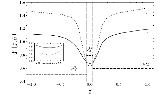
Figure 4: The cut of the spatial-temporal distribution of the concentration of vacancies along the growth axis at different times: 1 — at the moment ; 2 — ; ; ; ; [formula (12)]; .
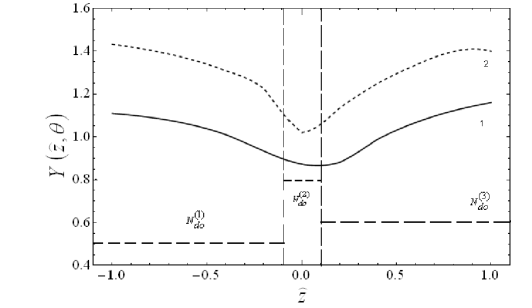
In figures 4 and 5, numerical calculations of the cut of the spatial-temporal distribution of the concentration of vacancies along the growth axis () of heterosystem at different times are presented: ; ; ( is the average time of finding the defect in one of the equilibrium positions in the interlayer nanoheterosystem, namely a settled life) and for the different thicknesses of the interlayer of a nanoheterostructure (, figure 4 and , figure 5).
Figure 5: The cut of the spatial-temporal distribution of the concentration of interstitial atoms along the growth axis at different times: 1 — at the moment ; 2 — ; ; ; ; [formula (12)]; .
As seen from figures 4 and 5, during the time interval there occurs a spatial-temporal redistribution of the defects, so that in the inhomogeneous-compressed interlayer [figure 1, region 2, formula (1)] they become smaller relative to their initial average value by at different times , , respectively. Starting from the time , there practically establishes a stationary state of the distribution of the defects in a three-layer stressed nanoheterosystem. Thus, the deformation field of the interlayer () clears away the workspace from the defects which finally makes the material of the workspace having a greater intensity of photoluminescence [10]. In exterlayers (figure 1, regions 1, 3) of the heterosystem, the concentration of the defects asymmetrically monotonously increases from the boundary of the contacting materials and becomes larger than their average value , .
If there are no defects () in the contacting materials, inhomogeneous deformation is created only due to a mismatch between the lattice parameters of contacting materials [], and in the absence of the mismatch between the lattice parameters (), the deformation [] is caused only by the point defects.
4 Conclusions
•
It has been established that the concentration profile of point defects at is of nonmonotonous character with a minimum in the middle of the interlayer InxGa1-xAs which is impoverished by the point defect of the type of compression centers when the interlayer of the heterostructure GaAs/InxGa1-xAs/GaAs undergoes an inhomogeneous compression, while in the case of inhomogeneous tension the opposite effect takes place. Thus, the deformation field and the number of the defects in the workspace of nanooptoelectronic devices can be controlled.
•
It is shown that if the ratio of the thickness of the middle layer to the thicknesses of the external layers of a nanoheterosystem GaAs/InxGa1-xAs/GaAs is , the ratio of the initial average concentrations of the vacancies in the layers of a nanoheterosystem is , , and the value of the deformation parameter is , then the established concentration of vacancies in the middle layer is less than the initial average concentration by 16 %. If the ratio , then the established concentration of the vacancies in the middle layer is larger than the initial average concentration . Such a reduction of the established concentration of the vacancies in the workspace of a nanoheterosystem is correlated with the experimental results of the work [10].
Appendix
To find the solution of differential equations (16) with boundary conditions (17), the integral Laplace transformation is used:
(18)
Then, the differential equation (16) and boundary conditions (17) take up the form:
(19)
(20)
where .
Analytical solutions of differential equations (19) in each layer are as follows:
(21)
Integration constants , , , are determined from the following system of algebraic equations:
(22)
By carrying out the inverse Laplace transformation we obtain the spatial-temporal redistribution of the point defects in the first, second and third stressed layers, respectively:
(23)
where functions , and are the solutions of differential equations (16) with boundary conditions (17), respectively:
[8]
Fracture Mechanics and Strength of Materials. Reference Guide in 4 volumes, vol. 3, Panasyuk V.V. (Ed.), Naukova Dumka, Kiev, 1988, p. 463 (in Russian).