Zigzag phosphorene nanoribbons: one dimensional resonant channels in two dimensional atomic crystals
Abstract
We theoretically investigate phosphorene zigzag nanoribbons as a platform for constriction engineering. In the presence of a constriction at one of the edges, quantum confinement of edge protected states reveals conductance peaks, if the edge is uncoupled to the other. If the constriction is narrow enough to promote coupling between edges, it gives rise to Fano-like as well as anti-resonances in the transmission spectrum. These effects are shown to mimic an atomic chain like behavior in a two dimensional atomic crystal.
pacs:
73.20.At , 73.22.-f, 73.23.-bI Introduction
Low dimensional systems have attracted the attention at least in the past fifty years, since the development of semiconductor epitaxial growth and deposition of metallic thin films Esaki and Tsu (1970). The early scenario, back in the 1960’s, as promising as it appeared, has evolved into a mainstream interest in condensed matter physics due to landmark discoveries in the late 1970s and early 1980s, like the quantum Hall effect Klitzing et al. (1980) and the conductive polymers Shirakawa et al. (1977), respectively 2D and 1D systems. The subsequent discovery of new carbon allotropes, showing stable structures either in 0D (fullerenes), 1D (carbon nanotubes) and 2D (graphene) consolidated this scenario in an exciting research field Hirsch (2010). The isolation of strictly one atom thick layers in the first years of the present century opened a wider window for both basic physics and device applications Novoselov et al. (2012). These new disruptive research efforts, initially impulsed by graphene, are nowadays detaching from carbon based roadmaps, as also envisaged, at the beginning of the graphene boost, by Novoselov, Geim and coworkers Novoselov et al. (2005).
A very recent 2D atomic crystal of black phosphorous Li et al. (2014); Koenig et al. (2014); Liu et al. (2014); Buscema et al. (2014), namely phosphorene, is a promising system in which 2D properties together with strictly 1D chain behavior are present in different energy windows, hence allowing to a same device to be tuned from a 1D to a 2D system by simply tuning the Fermi energy. In the present work we focus on the 1D energy window, created by effective doubly degenerate band (in the relevant energy scale) associated to states strongly localized at the zigzag edges Ezawa (2014); Carvalho et al. (2014) of phosphorene nanoribbons, whose properties are explored using a new strictly one dimensional resonant tunnelling device.
The double barrier resonant tunnelling device Esaki and Tsu (1970); Capasso et al. (1986); Chang et al. (1974), conceived here as an atomically precise segmentation at one of the edges, shows unusual geometry, since the direction of the barriers is perpendicular to the well and contact regionsWeisshaar et al. (1989); Wu et al. (1993). Among our findings we show that for a thin barrier case (constriction with narrow step from the upper zigzag edge), the resonant tunnelling permits a spectroscopy of the band structure of phosphorene nanoribbons in this energy window. Furthermore, progressive widening of the barriers (enhancing the step width of the constriction) therefore nearing the constriction to the other edge leads to edge coupling effects featuring resonances with Fano line shapes Miroshnichenko et al. (2010); Huang et al. (2015); Crespi et al. (2015) revealing also a new discrete/continuum states coupling system. For this latter coupled edge system, the transmission probability characteristics turn out to present clear features of both (i) the actual finite confining segment coupled to an infinite (not segmented) edge and, (ii) the properties of an infinite narrow nanoribbon with strongly coupled edges. These results are independent of the area of the device region, solely from the segmented region length and distance between the edges, revealing an effective chain-like behavior of the nanoribbon’s edges.
In what follows, we initially discuss the “bulk” electronic properties of a phosphorene nanoribbon, presenting the model calculation framework, as well as the effects of edge coupling on the conductance of these infinite zigzag ribbons that are essential to understand the resonant tunnelling spectra. Next, the geometry of the actual investigated segmented device is presented, introducing the resonant tunnelling effects. In the sequence, the core of the results is devoted to explore the segmented edge device resonant tunnelling behavior, showing how the defects on the edge may actually enrich the scenario instead of solely washing out the announced effects, giving further evidences that the phenomenon is restricted to the atoms at the very edge. Finally, the conclusions suggest a bridge between the present 1D systems embedded in a 2D crystal and ongoing research on isolated atomic chains.
II Phosphorene zigzag nanorribons and model calculation: edge coupling effects
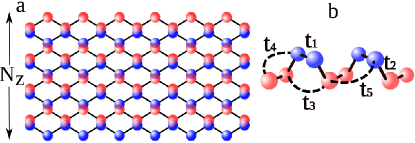
The essential atomistic aspects of the structures investigated are depicted in Fig. 1. Fig. 1(a) shows a segment of an infinite zigzag edged phosphorene nanoribbon of width = 8, the number of zigzag chains along the ribbon in this case. The tight binding hopping parameters considered, as discussed below, are indicated in Fig. 1(b).
The quite complex electronic structure of phosphorene, already at energy ranges rather close to the Fermi energy, hinders a wider use of single orbital tight-binding models in chasing the alluded electronic and transport properties of systems based on this new material. Nevertheless, the use of such model is well validated, by means of comparisons with first principle electronic structure calculations Rudenko and Katsnelson (2014), for the very energy window of interest around the gap, namely a double central band. This central band for zigzag phosphorene nanorribons has been predicted for phosphorene Carvalho et al. (2014); Ezawa (2014) and is absent in Graphene. We use here the same tight-binding parametrization for phosphorene proposed by RudenkoRudenko and Katsnelson (2014) considering a Hamiltonian , where () is the creation (annihilation) electronic operator at site and is the hopping integral between sites and . In this model, to characterize the low energy electronic properties five hopping integrals are required Rudenko and Katsnelson (2014): eV, = 3.665 eV, = -0.205 eV, =-0.105 eV and = -0.055 eV . The transmission is calculated using the recursive Green’s function Lewenkopf and Mucciolo (2013) in the phosphorene lattice representation. The left and right contacts broadening function and the self-energy of contact are calculated recursively for the semi-infinite zigzag phosphorene nanoribbons Sancho et al. (1985); other electronic properties such as the local density of states (LDOS) are also calculated.
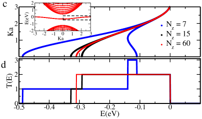

The electronic and transport properties of a host zizgzag nanoribbon in which a finite segment will be latter tailored in are also summarized in Fig. 1. The inset in Fig. 1(c) depicts the energy window of interest, showing the top(bottom) of the valence(conduction) band and an effectively degenerate central band Ezawa (2014). These central bands present cosine like dispersions characteristic for 1D systems Ezawa (2014). Indeed, the degeneracy comes from the fact that the width of the ribbon here is = 60, which guaranties that the two edges are effectively uncoupledTaghizadeh Sisakht et al. (2015). Hence this width will be chosen for the host ribbon where the constriction will be introduced.
The effect of edges coupling on the band structure can be followed in the main part of Fig. 1(c), showing a zoom of the central band energy range. Having in mind the uncoupled limit of = 60 (red curve), lifting of the central band effective degeneracy starts (in the present relevant energy scale) for = 15 (black curve) at the center of the Brillouin zone with an approximately symmetric splitting of slightly deformed cosine-like bands. Indeed an incipient overlap of wave function in this situation is illustrated in Fig. 1(e), with a noticeable amplitude of the wave function in the atomic sites well inside the ribbon (It should be noticed that corresponds to the number of zigzag chains, hence for =15, there will be 30 atomic sites in the unit cell). For extremely thin ribbons, = 7, the splitting becomes of the order of the uncoupled band widths (blue curve). More striking is the drastic change in the shape of one of the bands, showing a local maximum at the center at = 0 and a minimum at = 1.
The consequences of the edge coupling on the transmission probabilities along the edges are qualitatively significant as can be seen coming back to Fig. 1(d). Degenerate bands sum up to a plateau of = 2 (red curve). A slight lifting of the degeneracy breaks the lower threshold of the plateau introducing a = 1 step, an energy range where there is only one conduction channelEzawa (2014). However, extreme coupling leads to a = 3 plateau for , where the different states corresponding to the same energy in this band are added to the channel associated to the other cosine-like band.
III Segmented nanorribons: resonant tunnelling in 1d effective chains structures
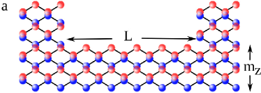
In the energy energy range of the edge states band, the “bulk” of the nanoribbon acts mainly as “in plane” substrate for the two dimensional channels at the edges. This condition, evidenced by the electronic band structure discussed in the previous section raises the question of a mean to observe experimentally those effective one-dimensional chains embedded in the rather complex phosphorene crystalline structure. In order to test our hypothesis we propose the segmented nanoribbon structure (constriction) illustrated in Fig. 2(a). The segment of a thinner region of the nanoribbon of width , also given in number of zigzag chains, is defined by a length in units of atoms removed along one zigzag direction. One essential parameter is the step width between the semi infinite upper edges and the central segment, which is simply defined as and, as will be seen below, defines the barrier thickness in the resonant tunnelling.
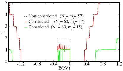
shows the transmission probabilities through two constrictions of lenght with and step widths, compared to a bare nanorribon, as a function of energy. In order to avoid any coupling between the edge states the width of the nanoribbon in the contacts is also . Transmission plateaus above (below) the edge states band are shown, for the sake of completeness, since these structures are of entirely different character than the resonances in the central band we will be focusing on. These transmission plateaus are due to the lateral confinement in a nanoribbon. This is confirmed by the green curve for , a deep step leading to a large shifting of the valence and conduction bands transmission plateaus, evidencing also the well known Fabry-Perot oscillationsSzafer and Stone (1989) due to the geometrical modulation; these effects are already well known for graphene and square lattice nanorribons with constrictions Wakabayashi and Sigrist (2000); Wakabayashi (2001); Muñoz Rojas et al. (2006); Yannouleas et al. (2015); Szafer and Stone (1989).
On the other hand, the edge states, observed here in the energy range from 0.3 eV to 0, drops to =1 with resonant peaks on top for wide constrictions and anti-ressonances for narrow constrictions. Fig. 3(a) presents a closer look at this energy range; for thin armchair steps () the red curve shows a group of 10 peaks, these resonances get thinner as the step increases (). Further diminishing , the barriers to the upper edge contacts become too large, but now the coupling to the lower edge becomes relevant. For transmission shows asymmetric Fano-like resonances at the low energy side and sharp anti-resonances at higher energies within the central band as will be discussed below. It should be recalled here that only for extremely thin nanoribbons the strong coupling between the edges widens the central band, however, it is not observed in Fig. 3(b) a plateau enlargement for because the edges of the left and right contact are not coupled (keeping the central band of the contacts unaltered).
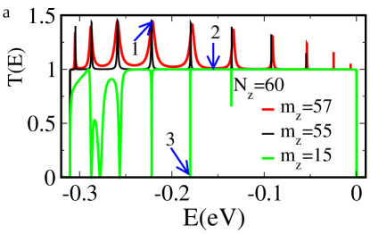
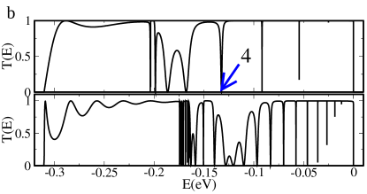
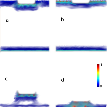
In our constriction the role of both channels (discrete states and continuum at the upper and lower edges respectively) can be made explicit by picturing the local density of states (LDOS) in Fig. 4, at the energy values indicated by arrows 1, 2, 3 and 4 in Fig. 3.
In Fig. 4(a), looking at the LDOS corresponding to a transmission peak pointed out by the arrow 1, it is clear that the higher values of LDOS appear on the edges, the confined state at the constriction in the upper edge clearly stands out. It should be noticed that this LDOS is slightly asymmetric, since the structure with equal to an even number of atoms is asymmetric (see Fig. 2(a)). This asymmetry leads to a resonance peak Buttiker (1988) superposed to the background plateau. equals to an odd number of atoms restore complete symmetry, leading to higher resonances, (not shown here). A less intense LDOS along the lower edge corresponding to the plateau can also be observed. The LDOS along the upper edge outside the constriction region is less intense in the figure scale, due to the prominence of the confined state. Far from a resonance, actually between two resonances, situation pointed out by arrow 2 in Fig. 3(a), the LDOS in the confined part of the upper edge is strongly suppressed, enhancing the contribution along the entire lower edge and the upper edge contact sections (i.e., outside the confining region), Fig. 4(b).
A quite different situation is depicted in Fig. 4(c)-(d), where the confined sate in the constriction is decoupled from the upper edge with a varible coupling to the lower edge. In Fig. 4(c), corresponding to the anti-resonance labelled as 3 in Fig. 3, we observe a faint coupling to the lower edge.
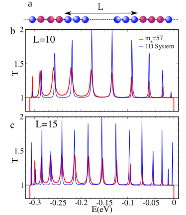
The LDOS plots reveal the unique character of the resonances observed in Fig. 3: resonant tunnelling through confined edge states in the constriction defined by an armchair-like step double barrier structure. It should be noticed that the number of resonances is identical to the number of atoms removed along the segment that define the length of the constriction, = 10, indicating that the transmission shows a spectroscopy of the 1D states at the edge of the constriction. Indeed, increasing the length of the constriction will increase at the same proportion the number of the resonances (not shown here). The fact that the resonances are insensible to the constriction width (hence the area for a fixed length) is a further indication that we are dealing with a strictly 1D effect at the edges: albeit the underlying 2D crystal, the behavior revealed here is the one of an effective atomic chain. Here we should notice that the only signature of the underlying 2D crystal is given by the resonances widths. Recalling Fig. 1(e), the resonances near the bottom of the central band, , correspond to states which deeper penetrate in the bulk, hence the barriers defined by the device steps are less effective than for resonances at higher energies. Two dimensional structured systems, like nanorribons, present transmission probabilities with multi channel contributions that are mixed by the geometrical changes along the structureMendoza et al. (2008); Datta (2005). On the other hand, one dimensional systems present single channel transmission probabilities, that are described by s-like orbital chain models. In the present case, indeed, the positions of the transmission resonances are shown in Fig. 5 to be well reproduced by a simple one dimensional double barrier quantum well modelled by a chain of s-like orbitals Datta (2005); Schulz and Gonçalves da Silva (1987). The nearest neighbor hopping () of the one dimensional chain, shown in Fig. 5(a), is calculated by eV, where is the edge states band width obtained from the red curve in Fig. 1(c). The transmission peaks of the one dimensional quantum well with and atomic sites clearly reproduce the position of the resonaces observed for phosphorene constrictions of the same length, see Fig. 5(b)-(c). The resonant peaks appear at the energies of the infinite square well energies for
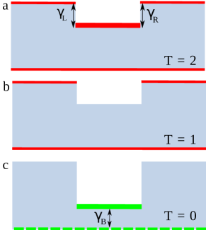
To recap, the edge states at opposite edge provide one dimensional electronic transport channels embedded in a two dimensional material and the conductance observed can be understood from simple model. The resonant peaks on top of the plateau resemble the conductance of two parallel and independent channels, as shown in Fig. 6(a). The lower edge provides a continuous channel of while the upper edge presents a quantum well with tunnelling coefficients accross the left(right) barrier defined by the vertical edges in the figure. Hence, resonant tunneling becomes only possible when the energy matches the energy of the bound states in the well. When this situation is not fulfilled the upper channel is closed and the transmission of the whole system is , see Fig. 6(b). A deeper step on the constriction, on the other hand, would lead to quasi bound states, i.e., wider barriers, connected to the upper edge contacts, but with a significant coupling, , to the bottom edge, Fig. 6(c), leading to Fano-like resonances and antiresonances in the transmission Guevara et al. (2003); Bahamon et al. (2015). This situation corresponds to quasi -bound state coupled to a continuum, leadind to fano-like asymmetric resonances and antiresonances in the transmission.
The three different line-shapes can be described by a single expression Huang et al. (2015):
| (1) |
where is the direct transmission without the presence of a scattering region, , ( is the energy of the resonant discrete state and its line width) and is the Fano asymmetry factor,which represents the ratio of the resonant tunneling channel to the channel due to the continuum (here represented by the lower edge channel). When and (no continuum channel available) a a resonance peak develops; for (both channels are relevant), an asymmetric line shape is revealed, while for an antiresonance appears.
Recalling the framework of the present work, edge confined states are supported only by zigzag edges, being absent in armchair or bearded edges Ezawa (2014); Carvalho et al. (2014). Therefore, introducing perturbations to a zigzag edge, like edge vacancies, would locally destroy these 1D states. The consequences of these perturbations are very relevant in the present early stage of phosphorene experimental development, in which only preliminary steps toward design and realization of effective devices out of the bulk in the nanoscale have been reported so far.Tayari V. et al. (2015). Hence, effects of the presence of disorder at the edges have to be considered.
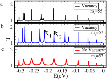
In Fig. 7 we present the transmission probability as a function of energy as well as LDOS associated to selected resonances in the presence of vacancies.
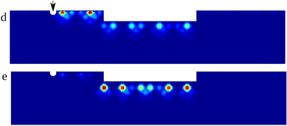
Defects are normally seen as mechanisms that hinder the observation of transport properties associated to shape modulation of nanoscopic low dimensional systems. Indeed, the resonance spectra are also dramatically modified in the present case. However, the issue can be seen from an entirely different point of view. The vacancies change locally the character of the edge, introducing actually small barriers, further dividing the system into smaller segments. The system chosen here is a device with a vacancy located at the upper edge of the left contact near the central segment (quantum well), the exact position is marked by the arrow in Fig. 7(d). What can be observed in the transmission probabilities in Fig. 7(a)-(c) is that the resonances of the well at the contact defined to the left by a barrier due to the vacancy, couple to some of the states of the original well given by the central segment. Those couplings are identified by the split peaks clearly seen in Fig. 7(b). If the barriers defining the central segment(well) are widened, Fig. 7(a), the splitting diminishes. Fig. 7(c) depicts the same device in absence of the vacancy as a guide for identifying the couplings. The character of the 1D confined states in the presence of a vacancy is illustrated in the LDOS, Fig. 7(d)-(e), for the resonances corresponding to arrows 1 and 2 in Fig. 7(b), respectively. State 1 corresponds to a double-well (vacancy-upper edge contact-left step-central segment-right step) along the upper edge, exhibiting LDOS at both wells, while state 2 is confined mainly to the central quantum well.
Having in mind the previous discussion, while a resonant tunnelling spectroscopy would become rather involved with the presence of defect induced barriers, scanning probe microscopy continues a way to reveal the edge quantum confinement.
IV Conclusions
It is inevitable to compare our results with those obtained for graphene constrictions: both zigzag graphene and phosphorene nanoribbons support edge states, however, their signatures on the electronic transport properties are completely different. First, edge states in zigzag graphene nanoribbons are sublattice polarized, so one single edge do not contribute to the electron transport properties. The graphene edge states channel is originated by the overlapping of edge states on opposite edges Wakabayashi et al. (2009), contrary to what we observe here where a single phosphorene edge provides an independent transport channel. Second, localized states in graphene junctions manifest as antiresonances of zero conductance, these states localize over the junction Wakabayashi and Sigrist (2000); Wakabayashi (2001); Muñoz Rojas et al. (2006), while the localized states of phosphorene constrictions strictly on grooved zigzag edge and appears as peaks, asymmetric Fano line shapes or dips in the conductance. In summary, we propose phosphorene zigzag nanorribons as a platform for constriction (segment) engineering. In the presence of an engraved segment at the upper edge, quantum confinement of edge protected states reveals resonant tunnelling transmission peaks if the upper edge of the host nanoribbon is uncoupled to the lower edge. Coupling between edges in thin constrictions give rise to Fano-like and antiresonances in the transmission spectrum of the system. One could envisage to look these effects by means of transport measurements as well as scanning probe microscopy Rivero et al. (2015). The energy scale given by the resonance spacing is of the order of 10 meV for constriction lengths of =30 (not shown here), corresponding to nm and contacts nm wide, a benchmark for experimental efforts, recalling that defects may lead to more complex spectra without washing out the main features. Other resonant tunnelling mechanisms have been observed in phosphorene nanoribbons with vacancies Srivastava et al. (2015), defects Umar Farooq et al. (2015) and transverse electric fields Wu et al. (2015). It is important to reinforce that these mechanisms involve states at the interior of the nanoribbon, whereas the effect shown here requires one dimensional states localized at the edges.
Concomitant to the development of the fascinating physics of 2D materials, new extreme 1D systems, namely isolated atomic chains, either based on Carbon Jin et al. (2009) or metallic elements Nadj-Perge et al. (2014), have been obtained and characterized, with their properties and possible applications theoretically investigated. The present results suggest a way were effective atomic chains come out from the edges of a 2D crystal.
Acknowledgments
CJP and ALCP acknowledge FAPESP, grant 2012/19060-0. DAB acknowledges support from FAPESP grant 2012/50259-8. PAS acknowledges support from CNPq. Numerical simulations were performed at cluster LaSCADo-UNICAMP, supported by FAPESP under project 2010/50646-6.
References
- Esaki and Tsu (1970) L. Esaki and R. Tsu, IBM Journal of Research and Development 14, 61 (1970).
- Klitzing et al. (1980) K. v. Klitzing, G. Dorda, and M. Pepper, Physical Review Letters 45, 494 (1980).
- Shirakawa et al. (1977) H. Shirakawa, E. J. Louis, A. G. MacDiarmid, C. K. Chiang, and A. J. Heeger, J. Chem. Soc., Chem. Commun. , 578 (1977).
- Hirsch (2010) A. Hirsch, Nat Mater 9, 868 (2010).
- Novoselov et al. (2012) K. S. Novoselov, V. I. Falko, L. Colombo, P. R. Gellert, M. G. Schwab, and K. Kim, Nature 490, 192 (2012).
- Novoselov et al. (2005) K. S. Novoselov, D. Jiang, F. Schedin, T. J. Booth, V. V. Khotkevich, S. V. Morozov, and A. K. Geim, Proceedings of the National Academy of Sciences of the United States of America 102, 10451 (2005).
- Li et al. (2014) L. Li, Y. Yu, G. J. Ye, Q. Ge, X. Ou, H. Wu, D. Feng, X. H. Chen, and Y. Zhang, Nat Nano 9, 372 (2014).
- Koenig et al. (2014) S. P. Koenig, R. A. Doganov, H. Schmidt, A. H. Castro Neto, and B. Özyilmaz, Applied Physics Letters 104, 103106 (2014).
- Liu et al. (2014) H. Liu, A. T. Neal, Z. Zhu, Z. Luo, X. Xu, D. Tománek, and P. D. Ye, ACS Nano 8, 4033 (2014).
- Buscema et al. (2014) M. Buscema, D. J. Groenendijk, S. I. Blanter, G. A. Steele, H. S. J. van der Zant, and A. Castellanos-Gomez, Nano Letters 14, 3347 (2014).
- Ezawa (2014) M. Ezawa, New Journal of Physics 16, 115004 (2014).
- Carvalho et al. (2014) A. Carvalho, A. S. Rodin, and A. H. C. Neto, EPL (Europhysics Letters) 108, 47005 (2014).
- Capasso et al. (1986) F. Capasso, K. Mohammed, and A. Y. Cho, Quantum Electronics, IEEE Journal of 22, 1853 (1986).
- Chang et al. (1974) L. L. Chang, L. Esaki, and R. Tsu, Applied Physics Letters 24, 593 (1974).
- Weisshaar et al. (1989) A. Weisshaar, J. Lary, S. M. Goodnick, and V. K. Tripathi, Applied Physics Letters 55, 2114 (1989).
- Wu et al. (1993) J. C. Wu, M. N. Wybourne, A. Weisshaar, and S. M. Goodnick, Journal of Applied Physics 74, 4590 (1993).
- Miroshnichenko et al. (2010) A. Miroshnichenko, S. Flach, and Y. Kivshar, Rev. Mod. Phys. 82, 2257 (2010).
- Huang et al. (2015) L. Huang, Y.-C. Lai, H.-G. Luo, and C. Grebogi, AIP Advances 5, 017137 (2015).
- Crespi et al. (2015) A. Crespi, L. Sansoni, G. Della Valle, A. Ciamei, R. Ramponi, F. Sciarrino, P. Mataloni, S. Longhi, and R. Osellame, Physical Review Letters 114, 090201 (2015).
- Rudenko and Katsnelson (2014) A. N. Rudenko and M. I. Katsnelson, Physical Review B 89, 201408 (2014).
- Lewenkopf and Mucciolo (2013) C. Lewenkopf and E. Mucciolo, Journal of Computational Electronics 12, 203 (2013).
- Sancho et al. (1985) M. P. L. Sancho, J. M. L. Sancho, J. M. L. Sancho, and J. Rubio, Journal of Physics F: Metal Physics 15, 851 (1985).
- Taghizadeh Sisakht et al. (2015) E. Taghizadeh Sisakht, M. H. Zare, and F. Fazileh, Physical Review B 91, 085409 (2015).
- Szafer and Stone (1989) A. Szafer and A. D. Stone, Physical Review Letters 62, 300 (1989).
- Wakabayashi and Sigrist (2000) K. Wakabayashi and M. Sigrist, Physical Review Letters 84, 3390 (2000).
- Wakabayashi (2001) K. Wakabayashi, Physical Review B 64, 125428 (2001).
- Muñoz Rojas et al. (2006) F. Muñoz Rojas, D. Jacob, J. Fernández-Rossier, and J. J. Palacios, Physical Review B 74, 195417 (2006).
- Yannouleas et al. (2015) C. Yannouleas, I. Romanovsky, and U. Landman, The Journal of Physical Chemistry C 119, 11131 (2015).
- Buttiker (1988) M. Buttiker, IBM Journal of Research and Development 32, 63 (1988).
- Mendoza et al. (2008) M. Mendoza, P. A. Schulz, R. O. Vallejos, and C. H. Lewenkopf, Phys. Rev. B 77, 155307 (2008).
- Datta (2005) S. Datta, Quantum Transport atom to transistor (Cambridge University Press, 2005) cambridge Books Online.
- Schulz and Gonçalves da Silva (1987) P. A. Schulz and C. E. T. Gonçalves da Silva, Phys. Rev. B 35, 8126 (1987).
- Guevara et al. (2003) M. L. L. d. Guevara, F. Claro, and P. A. Orellana, Physical Review B 67, 195335 (2003).
- Bahamon et al. (2015) D. A. Bahamon, Z. Qi, H. S. Park, V. M. Pereira, and D. K. Campbell, Nanoscale 7, 15300 (2015).
- Tayari V. et al. (2015) Tayari V., Hemsworth N., Fakih I., Favron A., Gaufres E., Gervais G., Martel R., and Szkopek T., Nat Commun 6 (2015).
- Wakabayashi et al. (2009) K. Wakabayashi, Y. Takane, M. Yamamoto, and M. Sigrist, New Journal of Physics 11, 095016 (2009).
- Rivero et al. (2015) P. Rivero, C. M. Horvath, Z. Zhu, J. Guan, D. Tománek, and S. Barraza-Lopez, Phys. Rev. B 91, 115413 (2015).
- Srivastava et al. (2015) P. Srivastava, K. P. S. S. Hembram, H. Mizuseki, K.-R. Lee, S. S. Han, and S. Kim, The Journal of Physical Chemistry C 119, 6530 (2015).
- Umar Farooq et al. (2015) M. Umar Farooq, A. Hashmi, and J. Hong, Scientific Reports 5, 12482 EP (2015).
- Wu et al. (2015) Q. Wu, L. Shen, M. Yang, Y. Cai, Z. Huang, and Y. P. Feng, Phys. Rev. B 92, 035436 (2015).
- Jin et al. (2009) C. Jin, H. Lan, L. Peng, K. Suenaga, and S. Iijima, Phys. Rev. Lett. 102, 205501 (2009).
- Nadj-Perge et al. (2014) S. Nadj-Perge, I. K. Drozdov, J. Li, H. Chen, S. Jeon, J. Seo, A. H. MacDonald, B. A. Bernevig, and A. Yazdani, Science 346, 602 (2014).