Imaging ambipolar two-dimensional carriers induced by the spontaneous electric polarization of a polar semiconductor BiTeI
Abstract
Two-dimensional (2D) mobile carriers are a wellspring of quantum phenomena. Among various 2D-carrier systems, such as field effect transistors and heterostructures, polar materials hold a unique potential; the spontaneous electric polarization in the bulk could generate positive and negative 2D carriers at the surface. Although several experiments have shown ambipolar carriers at the surface of a polar semiconductor BiTeI, their origin is yet to be specified. Here we provide compelling experimental evidences that the ambipolar 2D carriers at the surface of BiTeI are induced by the spontaneous electric polarization. By imaging electron standing waves with spectroscopic imaging scanning tunneling microscopy, we find that positive or negative carriers with Rashba-type spin splitting emerge at the surface correspondingly to the polar directions in the bulk. The electron densities at the surface are constant independently of those in the bulk, corroborating that the 2D carriers are induced by the spontaneous electric polarization. We also successfully image that lateral - junctions are formed along the boundaries of submicron-scale domains with opposite polar directions. Our study presents a novel means to endow non-volatile, spin-polarized, and ambipolar 2D carriers as well as, without elaborate fabrication, lateral - junctions of those carriers at atomically-sharp interfaces.
pacs:
73.20.At, 68.37.Ef, 71.70.EjI Introduction
The spontaneous electric polarization of polar materials causes surface charges, or band bending near the surface. If the band bending is large enough for the conduction and valence bands to cross the Fermi level, two-dimensional (2D) positive carriers can emerge at one side of a material and negative ones at the other side. Such mobile carriers, if realized, expand an arena of 2D-carrier systems that exhibit a wide variety of quantum phenomena Ando et al. (1982); Hwang et al. (2012). A pioneering work on BaTiO3 claimed that the electric conductivity was increased by the polarization Watanabe et al. (2008). However, carrier polarities were not shown and thus their relationship with the polarization is unclear. To clarify the relationship, it is necessary to carefully examine surface modifications, as emphasized in Ref. Watanabe et al., 2008. For example, oxygen vacancies created on the fractured surface produce a 2D electron gas at the surface of SrTiO3 (Ref. Santander-Syro et al., 2011; Wang et al., 2014). In contrast to the simple mechanism, it has never been established whether the spontaneous electric polarization actually induces 2D carriers.
A polar semiconductor BiTeI is an emergent candidate possessing the polarization-induced 2D carriers. BiTeI has a layered crystal structure with triple layers composed of Te, Bi, and I layers stacking along the -axis Tomokiyo et al. (1977); Shevelkov et al. (1995); Kanou and Sasagawa (2013), as shown schematically in Fig. 1(a). In this polar crystal structure, the spin degeneracy in the band structures is lifted by spin-orbit interaction Rashba (1960). Angle-resolved photoemission spectroscopy (ARPES) reveals that BiTeI indeed exhibits momentum-dependent (Rashba-type) spin splitting larger than ever reported Ishizaka et al. (2011); Crepaldi et al. (2012); Landolt et al. (2012); Sakano et al. (2013, 2012); Crepaldi et al. (2014). Because of this feature, BiTeI is proposed as a component for spintronics applications Tsutsui and Murakami (2012). In addition, both -type and -type two-dimensional (2D) band dispersions are observed at the surface of BiTeI Crepaldi et al. (2012); Landolt et al. (2012). Although preceding studies have shown the presence of band bending near the surface accompanied with the surface carriers Ishizaka et al. (2011); Crepaldi et al. (2012); Landolt et al. (2012); Eremeev et al. (2012), the origin of the band bending (and thus the origin of the surface carriers) remains elusive. Ishizaka el al. indicate similarity to near-surface electron-accumulation layers of semiconductors Ishizaka et al. (2011). Eremeev et al. suggest that the breaking translational symmetry at the surface with the strong ionicity modifies the electrostatic potential near the surface Eremeev et al. (2012). In contrast to these surface origins, Butler et al. speculate that the spontaneous electric polarization in the bulk causes the spectral shift to discuss the surface structures Butler et al. (2014). Actually, the surface structure necessary to identify the origin is also still obscure. Multiple termination layers hosting the ambipolar carriers are attributed to stacking faults (an excess or deficiency of an atomic layer) and steps Crepaldi et al. (2012), or opposite stacking sequences Landolt et al. (2012); Tournier-Colletta et al. (2014); Butler et al. (2014). Surface vacancies or absorbates have not been addressed in the preceding microscopy Tournier-Colletta et al. (2014); Butler et al. (2014).
In this study, we substantiate that the ambipolar 2D carriers at the surface of BiTeI are induced by the spontaneous electric polarization. A core challenge, defined by the previous studies, is to elucidate local electronic states including carrier polarities, together with surface structures from submicron- to atomic- scales. For this purpose, we performed spectroscopic-imaging scanning tunneling microscopy (SI-STM) which yields images of the local density of states (LDOS) by measuring spatial variation of the differential tunneling conductance, d/d. To determine local carrier polarity, we exploit electron standing waves appearing as spatial modulations in d/d images Hasegawa and Avouris (1993); Crommie et al. (1993). An electron standing wave is caused by quantum interference between electron waves incident to and elastically scattered from an atomic defect or step. The wavevector of electron standing wave is given as difference between those of original electron waves, . Therefore, the dispersion relationship , specifically the sign of d/d, directly reflects carrier polarity: negative for holes and positive for electrons.
II Methods
Single crystals of pristine and substituted BiTeI used in this study were grown by a modified Bridgman method Kanou and Sasagawa (2013). All samples are doped with electrons due to non-stoichiometry. Bulk electron densities are determined by the Hall coefficient measured at room temperature. The cm-3 samples are metal with temperature-independent electron densities Kanou and Sasagawa (2013); Horák et al. (1981). The Fermi levels of cm-3 samples lie 0.1 eV above the bulk conduction band minimum Lee et al. (2011); Murakawa et al. (2013); Wang et al. (2013). Meanwhile, since the cm-3 samples are not fully metallic and have the Fermi levels near the bulk conduction band minimum, their electron densities at low temperatures where SI-STM measurements were performed may be smaller than those at room temperature. Therefore, the 0.1 eV difference of the Fermi levels and the two orders of magnitude difference of the bulk electron densities are the minimum estimates of those at low temperatures.
For SI-STM measurements, BiTeI crystals were cleaved in an ultra-high vacuum chamber at 77 K. The crystals were then immediately transferred with a transfer rod cooled together with the crystals, through an insert cooled by liquid helium, to a home-built STM head placed at the bottom of the insert and cooled down to 4.6 K beforehand. All SI-STM measurements were carried out at 4.6 K with tungsten tips sharpened electrochemically and prepared with a field ion microscope. Bias voltages were applied to the sample and the tip was virtually grounded. Topographic images were taken in the constant-current mode. d/d spectra and images were measured by a standard lock-in technique with a setup current of 0.2 nA and the feedback loop opened. The modulation voltage was 5 mVrms unless otherwise noted. Fourier transforms of d/d images are symmetrized based on symmetry of BiTeI.
III Results
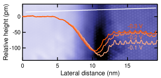
To grasp submicron-scale characteristics of BiTeI, we show a large topographic image in Fig. 1(b). A prominent structure observed in all samples studied is the two types of domains identified topographically and electronically as described below. The domains are typically several hundred nanometers in size and separated by depression in topographic images. The domain boundaries are not straight along the crystalline axes but meandering smoothly. One type of the domains is apparently higher than the other by about 0.1 nm, which weakly depends on bias voltages (Appendix A). The bias dependence means that the topmost layers of the domains are crystallographically inequivalent.
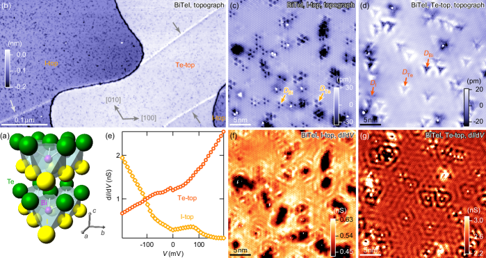
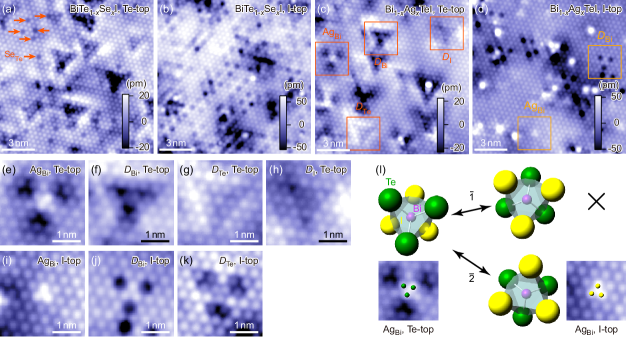
A topographic distinction between the two types of domains is defect patterns appearing in high-resolution topographic images shown in Fig. 1(c) and 1(d). Besides the triangular lattices with the bulk -axis constant, atomic defects are imaged as three dots in Fig. 1(c), but dark triangles in Fig. 1(d). The fact that only two kinds of domains are observed indicates that the domains are composed of opposite stacking sequences, I-Bi-Te (I-top) and Te-Bi-I (Te-top). (See Appendix B for detailed description.) More details about the domain structure are brought by further investigating topographic images. First, stacking sequences of each domain are I-top for Fig. 1(c) and Te-top for Fig. 1(d). Second, the structural relationship between the domains is (reflection about the (0001) plane). Third, central sites of defect patterns are identified as shown in Fig. 1(c) and 1(d). (See Appendix C for full descriptions.) These thorough identifications of the domain structure play an important role to understand electronic states of each domain as described below.
An electronic distinction between the two types of domains is represented by d/d spectra shown in Fig. 1(e). The spectrum of the Te-top domain shows finite conductance in the voltage range studied whereas that of the I-top domain shows vanishingly small conductance at positive bias voltages. The latter implies that, at the surface of the I-top domain, the top of valence band is located slightly above the Fermi level and thus the charge carriers are holes in contrast to electrons in the bulk. d/d images also clearly manifest the distinction as shown in Fig. 1(f) and 1(g). Electron standing waves are observed mainly near the defects on the I-top domain while all over on the Te-top domain SMd . By comparing these d/d images with the topographic images taken in the same location (Fig. 1(c) and 1(d)), we find that strong scattering centers are defects at Te-site in the I-top domain and Bi-sites in the Te-top domain.
To unambiguously conclude local carrier polarity of each domain, we focus on the dispersion relationships of the electron standing waves by analyzing Fourier transforms of d/d images as a function of bias voltages. In the I-top domain, a branch fans out from the point with decreasing bias voltages as shown in Fig. 2(a) and 2(b) SMF . The high-symmetry linecuts shown in Fig. 2(c)-2(f) exhibit a branch with negative slope (d/d) and crossing 0 mV as well as one more branch in deeper energies. Therefore, as implied by the d/d spectrum shown in Fig. 1(e), a 2D hole gas is formed at the surface of the I-top domain. Meanwhile in the Te-top domain, the dispersion relationship is completely different from that in the I-top domain. As shown in Fig. 2(g) and 2(h), two dispersive branches are observed. The outer branch appears as a peak in the direction and the inner one as a hexagonal ring surrounding the point. Both branches approach to the point with decreasing bias voltages SMF . The high-symmetry linecuts shown in Fig. 2(i)-2(l) exhibit that these branches have positive slope (d/d) and cross 0 mV. Therefore, the surface carriers of the Te-top domain are electrons. An energy-independent feature appearing on the outside of the outer branch is an extrinsic feature inherent to SI-STM because its location changes depending on setup bias voltages Kohsaka et al. (2007). We note that the identification of the top layer and corresponding dispersion relationships are consistent with the ARPES results Landolt et al. (2012).
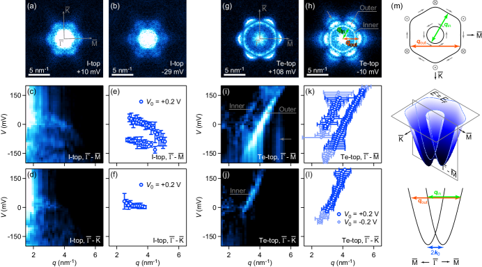
The clear electron standing waves in the Te-top domain bear closer analyses to unveil the nature of the electronic state. The presence of two branches indicates that two scattering channels connecting non-orthogonal electronic states are involved with the electron standing waves Petersen and Hedegård (2000); Pascual et al. (2004); Roushan et al. (2009). By comparing the observed dispersions with the ARPES results Ishizaka et al. (2011); Crepaldi et al. (2012); Landolt et al. (2012); Sakano et al. (2013), we assign the scattering channels in the Te-top domain as illustrated in Fig. 2(m). The inner branch arises from inter-band scattering between the spin-split bands as had ever been observed for Rashba-split states Hirayama et al. (2011); El-Kareh et al. (2013). The outer branch originates from intra-band scattering in the hexagonally-warped outer band. This branch emerges, as known for the surface Dirac Fermions of topological insulators Zhang et al. (2009); Fu (2009); Alpichshev et al. (2010); Beidenkopf et al. (2011), because of a non-zero out-of-plane component of the spin polarization that is characteristic of -symmetry of the crystal lattice Ishizaka et al. (2011); Bahramy et al. (2012). Given this assignment of the two branches, we can estimate the momentum offset of the spin-split bands at ( nm-1. This value agrees well with the ARPES results Ishizaka et al. (2011); Crepaldi et al. (2012); Landolt et al. (2012); Sakano et al. (2013). The spin splitting is observable in the electron standing waves of spin-split bands (without scattering to additional bandsSteinbrecher et al. (2013); Leicht et al. (2014)) when the band structure deviates from a simple Rashba model of a theoretical prediction Petersen and Hedegård (2000) and is hexagonally warped.
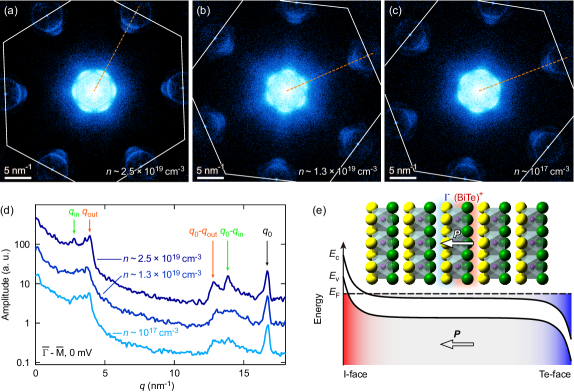
The most salient feature of the electron standing waves in the Te-top domain is found in relationship to bulk electron density, . As shown in Fig. 3(a)-3(d), the Fourier transforms of d/d images reveal that the wavevectors of two branches are independent of . This feature was commonly observed in the samples studied and thus is also independent of details of the domain structures. The constant wavevector means that, as the Fermi level shifts as changes (0.1 eV for the range studied Lee et al. (2011)), the surface band also shifts such that the Fermi wavelength of the surface 2D state stays constant. As indicated by the constant Fermi wavelength, the electron densities at the surface stay constant, even though those in the bulk change by two orders of magnitude. The surface electron density is roughly estimated at cm-2. The peculiar -independence is essential for specifying the mechanism of the 2D carriers as discussed below.
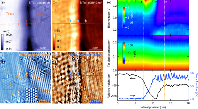
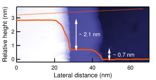
The electron standing waves are also observed around the domain boundary, providing details of the - junction at the boundary. Fig. 4(a) and 4(b) show a topographic and a d/d image taken in the same area around a domain boundary SMd . To highlight atomic-scale structures, we apply a Fourier filter suppressing long-wavelength structures. A structural model of the boundary is suggested from a filtered topographic image shown in Fig. 4(c). (See Appendix D for details.) The electron standing waves in both domains are better visualized in a filtered d/d image shown in Fig. 4(d) SMd , indicating that this - junction is a tunnel diode between highly-doped semiconductors. The depletion layer of the - junction manifests itself as the intervening zone without electron standing waves in Fig. 4(d).
Transition of the electronic states across the - junction is summarized in Fig. 4(e). d/d spectral variation occurs in the intervening zone, defining the depletion layer. The width of depletion layer is about 6 nm, in agreement with a simple estimate. (See Appendix E for details.) The depression observed in the topographic image corresponds to the depletion layer. The work function has three characteristics; it has larger value in the I-top domain, shows larger modulations in the I-top domain, and changes solely in the Te-top domain side of the depletion layer. The larger value is related to the origin of the ambipolar 2D carriers as described later as well as apparent heights of the domains (Appendix F). Further analysis is required for the larger modulations and the asymmetric change.
IV Discussion
How can the ambipolar 2D carriers be induced at the surface of BiTeI? The key ingredient to specify the origin is the peculiar constant density of the 2D electrons. Similar constant density is reported for SrTiO3 where the 2D electrons are attributed to surface oxygen vacancies Santander-Syro et al. (2011). In this case, the density of oxygen vacancies at the surface is much larger than and virtually independent of that in the bulk. In contrast, however, extrinsic surface modifications are not observed in our samples (Appendix G) and therefore excluded as the origin of the 2D carriers. Instead, the constant density in BiTeI is naturally explained by the spontaneous electric polarization in the bulk. The unit BiTeI layer consists of a positively-charged (BiTe)+ bilayer and a negatively-charged I- layer Shevelkov et al. (1995). The spontaneous electric polarization therefore directs from a BiTe bilayer to an I layer within the unit layer. The conduction (valence) band then is bent negatively (positively) and split off to form a 2D electron (hole) gas at the surface of the Te-top (I-top) domain, as illustrated in Fig. 3(e). Since the density of accumulated 2D electrons is determined by strength of the polarization, it is independent of bulk electron density.
The other observations are also comprehensively understood by the spontaneous electric polarization. The work function larger in the I-top domain is consistent with stronger confinement of electrons into the bulk caused by the spontaneous electric polarization pointing from a BiTe bilayer to an I layer. The strong scattering at Bi-site (Te-site) in the Te-top (I-top) domain reflects the orbital character of the surface band split from the conduction (valence) band where Bi-6p (Te-5p) orbitals predominantly contribute Bahramy et al. (2012). The domain structure with the relationship and the meandering boundaries is analogous with those of displacive-type ferroelectrics. We thus conclude that the ambipolar 2D carriers at BiTeI surfaces are induced by the spontaneous electric polarization in the bulk.
In this study, we have precisely determined local carrier polarity by observing electron standing waves with SI-STM. This results demonstrates that, to probe carrier polarity, SI-STM is available complementarily to other techniques such as ARPES, thermoelectric probes, single electron transistors, and photoelectron emission microscopy. Moreover, we unveiled that the underlying mechanism of electron standing waves is common to that of Dirac Fermions in topological insulators. This enables us to examine Rashba-type spin splitting with SI-STM and provides a unified framework to address spin-dependent scattering phenomena that are a key aspect for spintronics applications. Most importantly, our study establishes that the spontaneous electric polarization induces ambipolar 2D carriers. Carrier densities of these 2D carriers may be controlled by strain and temperature via the piezoelectric and pyroelectric effects. Since the - junction at the domain boundary is a consequence of the ambipolar 2D carriers and the domain structure sharing the common root, the surface of a polar material is a new platform to investigate a lateral - junction of 2D carriers. Such a surface can be a potential substructure to study unconventional devices such as a topological - junction Wang et al. (2012). The spontaneous electric polarization is, as a means to induce 2D carriers, complementary to field effect transistors and heterostructures in the sense that the induced carriers are non-volatile and polarity-switchable, and thus is available to explore new phenomena and functionalities.
Acknowledgements.
We thank K. Ishizaka and M. Kawamura for fruitful discussions. This work was supported by JSPS KAKENHI Grant numbers 24340078 and 24684022.Appendix A Bias dependence of relative heights
Apparent heights of the two types of domains depend on the bias voltages as shown in Fig. 5, indicating that the electronic states at the surfaces of the domains are different and the electronic difference contributes to the difference of apparent heights. This is contrasting to a step where its height is independent of the bias voltages. See also Appendix F about contributions to the apparent height.
Appendix B Domains with opposite stacking sequences
The experimental fact that only two kinds of domains are observed means that number of surface structures is two. If there are multiple cleavage planes in the ideal crystal structure, more than two kinds of surface structures appear due to combinations of the topmost and subsurface layers. Stacking faults also give more than two kinds of surface structures for the same reason. Multiple cleavage planes and stacking faults are excluded also by the step heights that are multiples of the -axis lattice constant (Fig. 6). Then, the topmost layer of each domain must be one of the two layers adjacent to the natural cleavage plane, and the second-topmost layer must be one remaining layer. Namely, Te and I layers are the top and a Bi layer is the second. That is, the observed domain structures are composed of opposite stacking sequences, Te-Bi-I (Te-top) and I-Bi-Te (I-top). This domain structure naturally accounts for that spin polarization is observed to be unchanged even when a crystal is flipped Landolt et al. (2012), as suggested by the authors.
Appendix C Details about the domain structure
C.1 Identification of stacking sequence
To identify stacking sequences of the domains, we measured BiTe1-xSexI where Se substituted for Te works as a marker of Te site. As shown in Fig. 7(a) and 7(b), Se atoms are observed at the atomic site of Fig. 7(a), indicating that this type of domain with dark triangles has the Te-top stacking and the other with three dots has the I-top stacking.
C.2 Point-group operation between the domains
Here we consider the structural relationship between the two types of domains in terms of a point-group operation. As is evident from two topographic images taken on a single surface (Fig. 7(a) and 7(b), and Fig. 7(c) and 7(d)), the orientation of the topmost sublattices is identical for the two types of domains. Point-group operations to realize opposite stacking sequences with keeping orientation of the topmost sublattices are (inversion), (reflection), , and . Actually, only and are independent because of the three-fold crystal symmetry of BiTeI.
A distinction between and is given by locations of Bi atoms. With respect to the topmost sublattice, there are two possible sites where Bi atoms can occupy. If is the case, Bi atoms occupy the same site in both domains. If is the case, they occupy different sites. To make this distinction, we measured topographic images of Bi1-xAgxTeI as shown in Fig. 7(c) and 7(c). Since AgBi atoms are observed at different sites (Fig. 7(e)and 7(i)), the point-group operation is (reflection). The above discussion is summarized in Fig. 7(l). This successful identification of the domain structure demonstrates that a combination of crystal growth and scanning tunneling microscopy works complementarily to diffraction techniques and transmission electron microscopy to determine local structures.
C.3 Identification of defect patterns
Fig. 7(e)-7(k) show topographic patterns of defects and impurities. Identifying a defect pattern centered at the topmost Te atoms is straightforward (Fig. 7(g)). Although defects bright in color are often found at the topmost I site, we have not yet identified a feature common to all images of the I-top domain. Bi-site defects (Fig. 7(f) and 7(j)), found at an interatomic site, are identified based on locations of AgBi (Fig. 7(e) and 7(i)). Patterns centered at the other interatomic site are identified as remaining ones, I-site defects for the Te-top domain (Fig. 7), and Te-site defects for the I-top domain (Fig. 7(k)).
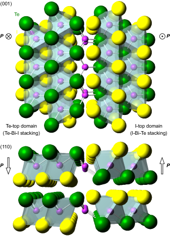
Appendix D A structural model of the domain boundary
Supplementary Figure 8 shows a structural model of the domain boundary. This model is constructed to satisfy the relationship between the domains and the lateral shift of the topmost sublattices shown in Fig. 4(c). As for a possible vertical shift of the domains, we can not separate a morphological height difference from the apparent height difference shown in the topographic image (Fig. 4(a)) because the LDOS and the work function also contribute to the apparent height. (See also Appendix F for a mathematical description.) The Bi sublattice, therefore, is drawn as flat for simplicity.
Appendix E Width of the depletion layer
Here we calculate the width of the depletion layer of a planer - junction, , with reasonable parameters to compare with the width of the observed depletion layer. is given by
| (1) |
where and are the vacuum permittivity and the electron charge, respectively. Others are material-dependent parameters. is the dielectric constant. is the built-in potential. and are the density of acceptors and donors, respectively. We use where is the 2D electron density on the Te-top domain. is estimated by the Fermi wavenumber and the wavenumber of the electron standing wave at 0 mV, . Namely, and . Since 2.8 nm-1, we get cm-3. Other parameters are (Ref. Lošťák et al., 1980) and 1.6 V that is estimated from the difference of the work function shown in Fig. 4(e). By using these values, we get nm.
Appendix F Apparent height in a topographic image
Here we give a simple mathematical description about multiple contributions to apparent height of a constant-current topographic image. The STM tunneling current is given by
| (2) |
while is the tip’s surface-normal coordinate, is the sample bias, and is the sample’s LDOS at lateral locations and energy . is related to the tunneling work function . , , and are the elementary charge, the electron mass, and the Planck constant, respectively. Given this formula, a constant-current () topographic image at a sample bias voltage is given by
| (3) |
Eq. (3) indicates that apparent height of a constant-current topographic image is low when the work function is large or the LDOS is small. This is a consequence of a feedback loop that gets a tip closer to a sample to compensate fast decay of the wave function or reduction of LDOS available for tunneling. In the case of BiTeI, the work function is larger in the I-top domain as shown in Fig. 4(e). The LDOS is likely to be smaller in the I-top domain because the 2D hole state in the I-top domain is caused by strong inversion whereas the 2D electron state in the Te-top domain by accumulation. Namely, both the work function and the LDOS contribute to the apparent height lower in the I-top domain.
Appendix G No extrinsic surface modification
Here we describe that our samples have neither surface absorbates nor additional defects possibly changing carrier density at the surface. As is evident in the topographic images shown in Fig. 1, no surface absorbate exists. Surface defects additionally generated by cleavage are excluded by counting the density of defects as follows.
To evaluate the density of defects near the surface, we assume that observed defects lie in the top unit layer. This assumption gives the highest estimate of defect density. By counting defects in several topographic images, we estimate that the density of these defects is about cm-3. This value, slightly larger than the bulk electron density ( cm-3), is just as expected because a considerable amount of acceptors exists in this material as well as predominant donors Horák et al. (1985). Therefore, the density of defects near the surface is virtually identical to that in the bulk without increased by cleavage.
References
- Ando et al. (1982) Tsuneya Ando, Alan B. Fowler, and Frank Stern, “Electronic properties of two-dimensional systems,” Rev. Mod. Phys. 54, 437–672 (1982).
- Hwang et al. (2012) H. Y. Hwang, Y. Iwasa, M. Kawasaki, B. Keimer, N. Nagaosa, and Y. Tokura, “Emergent phenomena at oxide interfaces,” Nat. Mater. 11, 103–113 (2012).
- Watanabe et al. (2008) Yukio Watanabe, Daisuke Matsumoto, Yosuke Urakami, T. Arai, A. Masuda, and S. W. Cheong, “Bipolar Carrier () Layer on Clean Surface of Insulating BaTiO3 Crystal Intrinsic to Ferroelectrics,” Ferroelectrics 367, 23–37 (2008).
- Santander-Syro et al. (2011) A. F. Santander-Syro, O. Copie, T. Kondo, F. Fortuna, S. Pailhès, R. Weht, X. G. Qiu, F. Bertran, A. Nicolaou, A. Taleb-Ibrahimi, P. Le Fèvre, G. Herranz, M. Bibes, N. Reyren, Y. Apertet, P. Lecoeur, A. Barthélémy, and M. J. Rozenberg, “Two-dimensional electron gas with universal subbands at the surface of SrTiO3,” Nature 469, 189–193 (2011).
- Wang et al. (2014) Zhiming Wang, Zhicheng Zhong, Xianfeng Hao, Stefan Gerhold, Bernhard Stöger, Michael Schmid, Jaime Sánchez-Barriga, Andrei Varykhalov, Cesare Franchini, Karsten Held, and Ulrike Diebold, “Anisotropic two-dimensional electron gas at SrTiO3(110).” Proc. Natl. Acad. Sci. USA 111, 3933–3937 (2014).
- Tomokiyo et al. (1977) Akihisa Tomokiyo, Toshihiro Okada, and Shigeaki Kawano, “Phase Diagram of System (Bi2Te3)-(BiI3)and Crystal Structure of BiTeI,” Jpn. J. Appl. Phys. 16, 291–298 (1977).
- Shevelkov et al. (1995) A. V. Shevelkov, E. V. Dikarev, R. V. Shpanchenko, and B. A. Popovkin, “Crystal Structures of Bismuth Tellurohalides BiTeX (X = Cl, Br, I) from X-Ray Powder Diffraction Data,” J. Solid State Chem. 114, 379–384 (1995).
- Kanou and Sasagawa (2013) Manabu Kanou and Takao Sasagawa, “Crystal growth and electronic properties of a 3D Rashba material, BiTeI, with adjusted carrier concentrations,” J. Phys. Condens. Matter 25, 135801 (2013).
- Rashba (1960) E. I. Rashba, “Properties of semiconductors with an extremum loop. 1. Cyclotron and combinational resonance in a magnetic field perpendicular to the plane of the loop,” Sov. Phys. Solid State 2, 1109–1122 (1960).
- Ishizaka et al. (2011) K. Ishizaka, M. S. Bahramy, H. Murakawa, M. Sakano, T. Shimojima, T. Sonobe, K. Koizumi, S. Shin, H. Miyahara, A. Kimura, K. Miyamoto, T. Okuda, H. Namatame, M. Taniguchi, R. Arita, N. Nagaosa, K. Kobayashi, Y. Murakami, R. Kumai, Y. Kaneko, Y. Onose, and Y. Tokura, “Giant Rashba-type spin splitting in bulk BiTeI,” Nat. Mater. 10, 521–526 (2011).
- Crepaldi et al. (2012) A. Crepaldi, L. Moreschini, G. Autès, C. Tournier-Colletta, S. Moser, N. Virk, H. Berger, Ph. Bugnon, Y. Chang, K. Kern, A. Bostwick, E. Rotenberg, O. Yazyev, and M. Grioni, “Giant Ambipolar Rashba Effect in the Semiconductor BiTeI,” Phys. Rev. Lett. 109, 096803 (2012).
- Landolt et al. (2012) Gabriel Landolt, Sergey V. Eremeev, Yury M. Koroteev, Bartosz Slomski, Stefan Muff, Titus Neupert, Masaki Kobayashi, Vladimir N. Strocov, Thorsten Schmitt, Ziya S. Aliev, Mahammad B. Babanly, J. Hugo Dil, Imamaddin R. Amiraslanov, Evgueni V. Chulkov, and Jürg Osterwalder, “Disentanglement of Surface and Bulk Rashba Spin Splittings in Noncentrosymmetric BiTeI,” Phys. Rev. Lett. 109, 116403 (2012).
- Sakano et al. (2013) M. Sakano, M. S. Bahramy, A. Katayama, T. Shimojima, H. Murakawa, Y. Kaneko, W. Malaeb, S. Shin, K. Ono, H. Kumigashira, R. Arita, N. Nagaosa, H. Y. Hwang, Y. Tokura, and K. Ishizaka, “Strongly Spin-Orbit Coupled Two-Dimensional Electron Gas Emerging near the Surface of Polar Semiconductors,” Phys. Rev. Lett. 110, 107204 (2013).
- Sakano et al. (2012) M. Sakano, J. Miyawaki, A. Chainani, Y. Takata, T. Sonobe, T. Shimojima, M. Oura, S. Shin, M. S. Bahramy, R. Arita, N. Nagaosa, H. Murakawa, Y. Kaneko, Y. Tokura, and K. Ishizaka, “Three-dimensional bulk band dispersion in polar BiTeI with giant Rashba-type spin splitting,” Phys. Rev. B 86, 085204 (2012).
- Crepaldi et al. (2014) A. Crepaldi, F. Cilento, M. Zacchigna, M. Zonno, J. C. Johannsen, C. Tournier-Colletta, L. Moreschini, I. Vobornik, F. Bondino, E. Magnano, H. Berger, A. Magrez, Ph. Bugnon, G. Autès, O. V. Yazyev, M. Grioni, and F. Parmigiani, “Momentum and photon energy dependence of the circular dichroic photoemission in the bulk Rashba semiconductors BiTeX (X=I, Br, Cl),” Phys. Rev. B 89, 125408 (2014).
- Tsutsui and Murakami (2012) Kazuhiro Tsutsui and Shuichi Murakami, “Spin-torque efficiency enhanced by Rashba spin splitting in three dimensions,” Phys. Rev. B 86, 115201 (2012).
- Eremeev et al. (2012) S. V. Eremeev, I. A. Nechaev, and E. V. Chulkov, “Giant Rashba-type spin splitting at polar surfaces of BiTeI,” JETP Lett. 96, 437–444 (2012).
- Butler et al. (2014) Christopher John Butler, Hung-Hsiang Yang, Jhen-Yong Hong, Shih-Hao Hsu, Raman Sankar, Chun-I Lu, Hsin-Yu Lu, Kui-Hon Ou Yang, Hung-Wei Shiu, Chia-Hao Chen, Chao-Cheng Kaun, Guo-Jiun Shu, Fang-Cheng Chou, and Minn-Tsong Lin, “Mapping polarization induced surface band bending on the Rashba semiconductor BiTeI,” Nat. commun. 5, 4066 (2014).
- Tournier-Colletta et al. (2014) C. Tournier-Colletta, G. Autès, B. Kierren, Ph. Bugnon, H. Berger, Y. Fagot-Revurat, O. V. Yazyev, M. Grioni, and D. Malterre, “Atomic and electronic structure of a Rashba - junction at the BiTeI surface,” Phys. Rev. B 89, 085402 (2014).
- Hasegawa and Avouris (1993) Y. Hasegawa and P. Avouris, “Direct observation of standing wave formation at surface steps using scanning tunneling spectroscopy,” Phys. Rev. Lett. 71, 1071–1074 (1993).
- Crommie et al. (1993) M. F. Crommie, C. P. Lutz, and D. M. Eigler, “Imaging standing waves in a two-dimensional electron gas,” Nature 363, 524–527 (1993).
- Horák et al. (1981) J. Horák, L. Tichý, and P. Lošťák, “Electrical conductivity of BiTeI crystals,” Phys. Status Solidi (a) 63, 407–416 (1981).
- Lee et al. (2011) J. Lee, G. Schober, M. Bahramy, H. Murakawa, Y. Onose, R. Arita, N. Nagaosa, and Y. Tokura, “Optical Response of Relativistic Electrons in the Polar BiTeI Semiconductor,” Phys. Rev. Lett. 107, 117401 (2011).
- Murakawa et al. (2013) H. Murakawa, M. S. Bahramy, M. Tokunaga, Y. Kohama, C. Bell, Y. Kaneko, N. Nagaosa, H. Y. Hwang, and Y. Tokura, “Detection of Berry’s Phase in a Bulk Rashba Semiconductor,” Science 342, 1490–1493 (2013).
- Wang et al. (2013) Chang-Ran Wang, Jen-Chuan Tung, R. Sankar, Chia-Tso Hsieh, Yung-Yu Chien, Guang-Yu Guo, F. C. Chou, and Wei-Li Lee, “Magnetotransport in copper-doped noncentrosymmetric BiTeI,” Phys. Rev. B 88, 081104 (2013).
- (26) See Supplemental Material at URL for bias dependence of the electron standing waves.
- (27) See Supplemental Material at URL for bias dependence of the Fourier-transform images.
- Kohsaka et al. (2007) Y Kohsaka, C Taylor, K Fujita, A Schmidt, C Lupien, T Hanaguri, M Azuma, M Takano, H Eisaki, H Takagi, S Uchida, and J C Davis, “An intrinsic bond-centered electronic glass with unidirectional domains in underdoped cuprates.” Science 315, 1380–1385 (2007), how the extrinsic feature appears is written in supporting online text 1. The denominator of Eq. (S6) results in a feature independent of energy and dependent of setpoint bias voltages.
- Petersen and Hedegård (2000) L. Petersen and P. Hedegård, “A simple tight-binding model of spin-orbit splitting of -derived surface states,” Surf. Sci. 459, 49–56 (2000).
- Pascual et al. (2004) J. Pascual, G. Bihlmayer, Yu. Koroteev, H.-P. Rust, G. Ceballos, M. Hansmann, K. Horn, E. Chulkov, S. Blügel, P. Echenique, and Ph. Hofmann, “Role of Spin in Quasiparticle Interference,” Phys. Rev. Lett. 93, 196802 (2004).
- Roushan et al. (2009) Pedram Roushan, Jungpil Seo, Colin V. Parker, Y. S. Hor, D. Hsieh, Dong Qian, Anthony Richardella, M. Z. Hasan, R. J. Cava, and Ali Yazdani, “Topological surface states protected from backscattering by chiral spin texture.” Nature 460, 1106–1109 (2009).
- Hirayama et al. (2011) Hiroyuki Hirayama, Yuki Aoki, and Chiaki Kato, “Quantum Interference of Rashba-Type Spin-Split Surface State Electrons,” Phys. Rev. Lett. 107, 027204 (2011).
- El-Kareh et al. (2013) L. El-Kareh, P. Sessi, T. Bathon, and M. Bode, “Quantum Interference Mapping of Rashba-Split Bloch States in Bi/Ag(111),” Phys. Rev. Lett. 110, 176803 (2013).
- Zhang et al. (2009) Tong Zhang, Peng Cheng, Xi Chen, Jin-Feng Jia, Xucun Ma, Ke He, Lili Wang, Haijun Zhang, Xi Dai, Zhong Fang, Xincheng Xie, and Qi-Kun Xue, “Experimental Demonstration of Topological Surface States Protected by Time-Reversal Symmetry,” Phys. Rev. Lett. 103, 266803 (2009).
- Fu (2009) Liang Fu, “Hexagonal Warping Effects in the Surface States of the Topological Insulator Bi2Te3,” Phys. Rev. Lett. 103, 256803 (2009).
- Alpichshev et al. (2010) Zhanybek Alpichshev, J. G. Analytis, J.-H. H. Chu, I. R. Fisher, Y. L. Chen, Z. X. Shen, A. Fang, and A. Kapitulnik, “STM Imaging of Electronic Waves on the Surface of Bi2Te3: Topologically Protected Surface States and Hexagonal Warping Effects,” Phys. Rev. Lett. 104, 016401 (2010).
- Beidenkopf et al. (2011) Haim Beidenkopf, Pedram Roushan, Jungpil Seo, Lindsay Gorman, Ilya Drozdov, Yew San Hor, R. J. Cava, and Ali Yazdani, “Spatial fluctuations of helical Dirac fermions on the surface of topological insulators,” Nat. Phys. 7, 939–943 (2011).
- Bahramy et al. (2012) M. S. Bahramy, B. J. Yang, R. Arita, and N. Nagaosa, “Emergence of non-centrosymmetric topological insulating phase in BiTeI under pressure,” Nat. Commun. 3, 679 (2012).
- Steinbrecher et al. (2013) Manuel Steinbrecher, Hasmik Harutyunyan, Christian R. Ast, and Daniel Wegner, “Rashba-type spin splitting from interband scattering in quasiparticle interference maps,” Phys. Rev. B 87, 245436 (2013).
- Leicht et al. (2014) Philipp Leicht, Julia Tesch, Samuel Bouvron, Felix Blumenschein, Philipp Erler, Luca Gragnaniello, and Mikhail Fonin, “Rashba splitting of graphene-covered Au(111) revealed by quasiparticle interference mapping,” Phys. Rev. B 90, 241406(R) (2014).
- Wang et al. (2012) Jing Wang, Xi Chen, Bang-Fen Zhu, and Shou-Cheng Zhang, “Topological - junction,” Phys. Rev. B 85, 235131 (2012).
- Lošťák et al. (1980) P. Lošťák, J. Horák, A. Vaško, and Nguyêñ tât Dich, “Optical Properties of BiTeI Crystals,” Phys. Status Solidi (a) 59, 311–316 (1980).
- Horák et al. (1985) J. Horák, P. Lošťák, L. Jansa, and P. Matoušek, “Departures from Stoichiometry of BiTeI Crystals Grown from the Vapour Phase,” Phys. Status Solidi (a) 89, 493–498 (1985).