The dielectric genome of van der Waals heterostructures
Abstract
Vertical stacking of two-dimensional (2D) crystals, such as graphene and hexagonal boron nitride, has recently lead to a new class of materials known as van der Waals heterostructures (vdWHs) with unique and highly tunable electronic properties. Ab-initio calculations should in principle provide a powerful tool for modeling and guiding the design of vdWHs, but in their traditional, form such calculations are only feasible for commensurable structures with a few layers. Here we show that the dielectric properties of realistic, incommensurable vdWHs comprising hundreds of layers can be calculated with ab-initio accuracy using a multi-scale approach where the dielectric functions of the individual layers (the dielectric building blocks) are coupled simply via their long-range Coulomb interaction. We use the method to illustrate the 2D-3D dielectric transition in multi-layer MoS2 crystals, the hybridization of quantum plasmons in large graphene/hBN heterostructures, and to demonstrate the intricate effect of substrate screening on the non-Rydberg exciton series in supported WS2.
The class of 2D materials which started with graphene is rapidly expanding and now includes metallic and semiconducting transition metal dichalcogenidesWang et al. (2012) in addition to group III-V semi-metals, semiconductors and insulatorsŞahin et al. (2009). These atomically thin materials exhibit unique opto-electronic properties with high technological potentialBritnell et al. (2013); Sup Choi et al. (2013); Shih et al. (2014); Woessner et al. (2015); Withers et al. (2015). However, the 2D materials only form the basis of a new and much larger class of materials consisting of vertically stacked 2D crystals held together by weak van der Waals forces. In contrast to conventional heterostructures which require complex and expensive crystal-growth techniques to epitaxially grow the single-crystalline semiconductor layers, vdWHs can be stacked in ambient conditions with no requirements of lattice matching. The latter implies a weaker constraint, if any, on the choice of materials that can be combined into vdWHs.
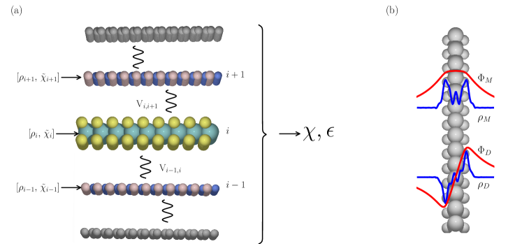
The weak inter-layer binding suggests that the individual layers of a vdWH largely preserve their original 2D properties modified only by the long range Coulomb interaction with the surrounding layers. Turning this argument around, it should be possible to predict the overall properties of a vdWH from the properties of the individual layers. In this Letter we show that this can indeed be achieved for the dielectric properties. Conceptually, this extends the Lego brick picture used by Geim and GrigorievaGeim and Grigorieva (2013) for the atomic structure of a vdWH, to its dielectric properties. Specifically, we develop a semi-classical model which takes as input the dielectric functions of the individual isolated layers computed fully quantum mechanically and condensed into the simplest possible representation, and couple them together via the Coulomb interaction, see Figure 1. Despite the complete neglect of interlayer hybridization, the model provides an excellent account of both the spatial and dynamical dielectric properties of vdWHs. The condensed representation of the dielectric function of all isolated 2D crystals can thus be regarded as the dielectric genome of vdWHs.
In addition to its conceptual value, our approach overcomes a practical limitation of conventional first-principles methods. Such methods are not only computationally demanding, but also rely on periodic boundary conditions which are incompatible with the incommensurable interfaces found in vdWHs. In fact, for many purposes, an in-plane lattice mismatch between neighbouring 2D crystals is preferred because it reduces the interlayer coupling and thus minimises the risk of commensurate-incommensurate transitionsWoods et al. (2014), and formation of Moire patternsKang et al. (2013) and associated band structure reconstructionsLu et al. (2014) which are typical for systems with similar lattice constants. This emphasises the need for alternative approaches for modelling vdWHs.
The dielectric function is one of the most important material response functions. It determines the effective interaction between charged particles in the material, contains information about the collective oscillations of the electron gas (plasmons)Pitarke et al. (2007), and enters as a fundamental ingredient in many-body calculations of e.g. excitons and quasiparticle band structuresOnida et al. (2002); Hybertsen and Louie (1986).
The (inverse) dielectric function is related to the electron density response function, , via
| (1) |
In our quantum-electrostatic heterostructure (QEH) model the calculation of the dielectric function is divided into two parts. In the first part the in-plane averaged density response function of each of the freestanding layers, , are obtained from ab-initio calculations. In practice we treat the in-plane momentum transfer, , as a scalar since most 2D materials are isotropic within the plane. From we calculate the magnitude of the monopole/dipole component of the density induced by a potential with a constant/linear variation across the layer and in-plane variation :
| (2) |
Here for the monopole and dipole components, respectively. In addition we calculate the spatial form of the induced density, . With a proper normalization of we can then write
| (3) |
We have found that while depends strongly on frequency, does not. The data set with or equivalently constitutes the dielectric building block of layer , as illustrated in Figure 1. According to Eq. (3) the dielectric building block allows us to obtain the density induced in the (isolated) layer by a constant/linear potential. It is straightforward to extend the dielectric building blocks to account for higher-order moments in the induced density described by , but we have found the dipole approximation to be sufficient in all cases considered.
In the second part of the QEH model, the density response function of the vdWH in the discrete monopole/dipole representation is obtained by solving a Dyson equation that couples the dielectric building blocks together via the Coulomb interaction. The Dyson equation for the full density response function giving the magnitude of the monopole/dipole density on layer induced by a constant/linear potential applied to layer , reads (omitting the and variables for simplicity)
| (4) |
The Coulomb matrices are defined as
| (5) |
where is the potential associated with the induced density, , which we calculate on a uniform grid by solving a 1D Poisson equation. Note that we leave out the self-interaction terms in Eq. (4) since the intralayer Coulomb interaction is already accounted for by the uncoupled . The (inverse) dielectric function of Eq. (1) in the monopole/dipole basis becomes
| (6) |
More details on the method and computations are provided in the supporting information.
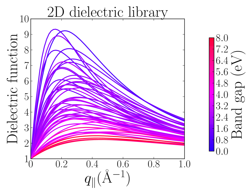
A database containing the dielectric building blocks of a large collection of 2D materials has been constructed, and is available from our website dat . It presently contains more than 50 transition metal dichalcogenides and oxides, graphene at different doping levels, and hBN, and more materials are being added. From here the data files can be downloaded together with a Python module for calculating the dielectric function and associated properties of any combination of these materials. QEH model calculations for vdWHs containing a few hundred layers can be performed on a standard PC. In Figure 2 we show the -dependent static dielectric functions of the monolayer transition metal dichalcogenides and -oxides presently contained in our database (for a complete overview of the materials see Ref. Rasmussen and Thygesen (2015)). All the dielectric functions show the same qualitative form, in particular they become 1 for and , however there is quite some variation in their magnitude. As expected the size of the dielectric function correlates well with the size of the band gap of the material indicated by the colour.
First-principles calculations were performed with the GPAW codeEnkovaara and et al. (2010); Yan et al. (2011). Single-particle wave functions and energies were calculated within the local density approximation (LDA) using 400 eV plane wave cut-off and at least sampling of the 2D Brillouin zone. Density response functions and dielectric functions were calculated within the random phase approximation (RPA). The RPA does not include electron-hole interactions, but generally yields good results for the static dielectric properties of semi-conductors and dynamical response of metals. Except for MoS2 bulk, we included at least 15 Å of vacuum in the super cells perpendicular to the layers and applied a truncated Coulomb kernel to avoid long range screening between periodically repeated structures. All response functions were calculated in a plane wave basis including reciprocal lattice vectors up to at least 50 eV. A similar cut off was used for the sum over empty states and convergence was carefully checked. The frequency dependence of the response functions was represented on a non-linear frequency grid ranging from 0 to 35 eV, with an initial grid spacing of 0.02 eV. All details of the calculations and atomic structure geometries are provided in the supporting information.
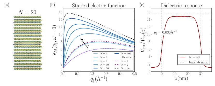
As a first application of the QEH model, we study how the (static) dielectric function of a 2D material evolves as the layer thickness increases towards the bulk. One of the most characteristic differences between 2D and 3D materials is the behaviour of the dielectric function in the long wave length limit: For a bulk semiconductor, the dielectric function tends smoothly to a constant value larger than unity as . In contrast for a 2D semiconductor implying a complete absence of screening in the long wave length limit Cudazzo et al. (2011); Hüser et al. (2013).
Ab initio calculations were performed for the dielectric function of MoS2 monolayer, bilayer, and bulk, and the QEH model was used for multilayer structures up to 100 layers. Figure 3 (b) shows the dielectric functions averaged over the slabs, i.e. the macroscopic dielectric function, as function of the in-plane momentum transfer. For large the dielectric functions show similar behavior. However, whereas for the bulk, the dielectric functions of the slabs decrease sharply to 1 for small . This demonstrates that the dielectric properties of a vdWH of thickness are 2D like for and 3D like for . Interestingly, also the result for bulk MoS2 shows reminiscence of the 2D nature of the constituent layers, where the magnitude of the dielectric function has a slight drop when .
The QEH model describes the change in the dielectric function from mono- to bilayer very accurately in spite of the well known differences between the mono- and bilayer band structuresCheiwchanchamnangij and Lambrecht (2012). This shows that hybridisation driven band structure effects, i.e. quantum confinement, have negligible influence on the dielectric properties of a vdWH and is the main reason for the success of the QEH model. The model result seems to converge towards the ab initio bulk result, however, convergence is not fully reached even for . The slow convergence towards the bulk result is mainly due to the spatial variation of the induced potential across the slab. In Figure 3 (c) we show the -dependent dielectric function defined as , for a constant (along ) external potential with a long wavelength in-plane variation for . Although is close to the ab-initio bulk value (dashed line) in the middle of the slab, screening is strongly suppressed in the surface region. Increasing the slab thickness beyond 50 layers brings the QEH result even closer to the bulk result in the middle of the slab, but a small underestimation remains originating from the difference in the band structures of the monolayer and bulk systems. The suppressed screening in the surface region is a direct consequence of the anisotropic nature of the layered MoS2 crystals which limits the screening of perpendicular fields relative to in-plane fields, and is expected to be a general property of vdWHs.
The model can also be used to calculate the response to fields polarized along the -direction, i.e. perpendicular to the layers. In this case the perpendicular component, , can be calculated by applying an external potential with a linear variation along . In the discrete basis of the QEH model, such a field is represented by a vector with 0 for all monopole components and 1 for all dipole components. Comparing the averaged slope of the total potential to the slope of the applied linear potential for a slab of N=100 layers of MoS2 yields . This value is somewhat larger than the bulk value of 6.03, however, due to long range surface effects it is not necessarily to be expected that the two numbers should coincide. In fact, we find excellent agreement between the QEH model and full ab-initio calculation of for a four layer MoS2 slab (see supporting information).
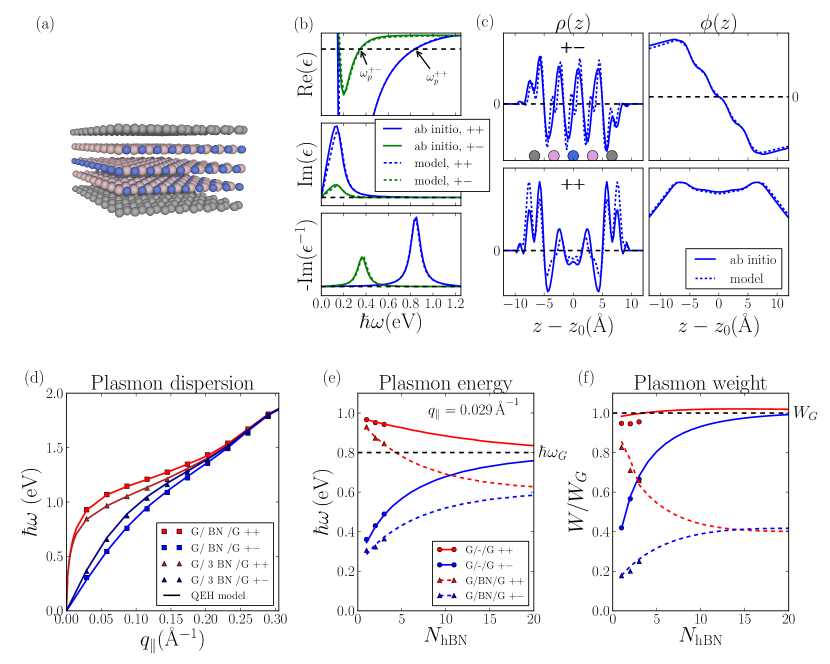
Next, we consider the hybridisation of plasmons in graphene sheets separated by hBN, see Figure 4(a). Plasmons in graphene on hBN were recently found to propagate with low loss Woessner et al. (2015), and the close to perfect lattice match between the two layers enables full ab initio calculations for the thinnest heterostructures. Here we use doped graphene that has a finite density of states at the Fermi level, giving rise to two-dimensional plasmons with energies in the regime 0-2 eV. The plasmon energies goes to zero in the optical limit, as is characteristic for plasmons in 2D metalsHwang and Sarma (2007); Shin et al. (2011). We calculate the effect of hBN on the plasmons using the QEH model for up to 20 layers of hBN and compare to full ab-initio calculations for 1-3 layers of hBN.
To identify the plasmons of the heterostructure we follow Ref. Andersen et al. (2012). In brief, we compute the eigenvalues, , of the heterostructure dielectric function for each frequency point and identify a plasmon energy, , from the condition , see Figure 4(b). The corresponding eigenvector, , represents the potential associated with the plasmon oscillation, see panel (c). This analysis identifies two plasmons corresponding to the symmetric () and antisymmetric () combinations of the graphene plasmons as previously found for two freestanding graphene sheets Hwang and Das Sarma (2009). For 1-3 hBN layers, the QEH model perfectly reproduces the ab-initio results for the dielectric eigenvalues, plasmon energy, and weight. The latter was defined as the area under the peaks in the loss function , see panel (b). The densities and potentials of the plasmon eigenmodes shown in panel (c) are also reproduced fairly accurately by the model, where the qualitative differences for the induced densities, , are due to the use of a limited basis of the monopole and dipole response for each layer. In panels (e-f) the result of full ab-initio calculations are shown by symbols while the QEH results are shown by continuous lines. The effect of the hBN buffer (dashed lines) is to red shift and damp the plasmons compared to the result for two graphene sheets separated by the same amount of vacuum (full lines). This is also reflected by the relatively large amount of electron density located on the hBN during the plasma oscillation, see panel (c).
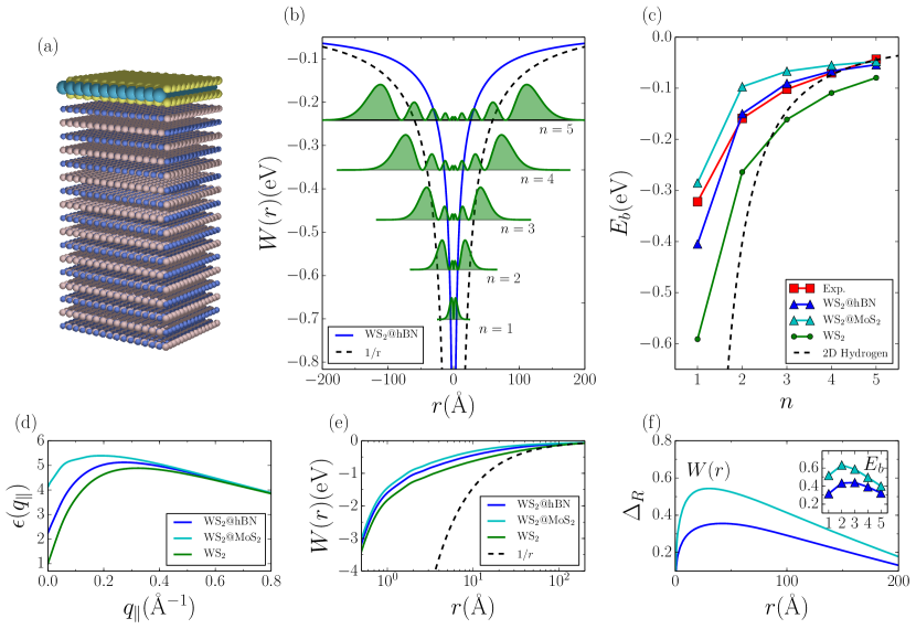
Finally, we explore some characteristic features of excitons in freestanding and supported 2D semiconductors. A straight forward generalisation of the well known Mott-Wannier modelWannier (1937) leads to the following eigenvalue equation for the excitons of a 2D semiconductorCudazzo et al. (2011); Berkelbach et al. (2013):
| (7) |
where is the exciton binding energy, is the wave function, is the effective mass, and is the screened electron-hole interaction. Assuming that the electron and hole are localised in layer 1, the Fourier transformed screened electron-hole interaction is obtained from the static () response function Eq. (4) and Coulomb interaction matrix Eq. (5) of the QEH model,
| (8) |
The first term is the bare, i.e. unscreened, electron-hole interaction in layer 1 under the assumption that the electron and hole densities can be represented by the induced monopole density, . The second term describes the screening from the surrounding layers and layer 1 itself. Note that the above equation can be easily generalised to describe the screened interaction between charges localised in different layers (relevant for indirect excitons).
In Ref. Chernikov et al. (2014) Chernikov et al. observed a peculiar non-hydrogenic Rydberg series for the excitons in a single layer of WS2 adsorbed on a SiO2 substrate. Here we use the QEH model to calculate the screened electron-hole interaction within the WS2 layer from the dielectric function of the full heterostructure. Since the QEH is applicable only to layered materials we place WS2 on a 100 layer thick slab of hBN which has dielectric constant very similar to that of SiO2 (both around 4). For comparison we performed similar calculations using MoS2 as substrate (dielectric constant larger than SiO2). Figure 5 (c) shows the five lowest -excitons calculated from Eq. (7) for both freestanding and supported WS2. For freestanding WS2, we obtain eV for the lowest exciton in good agreement with previous ab-initio calculationsShi et al. (2013). The enhanced screening from the substrate lowers the exciton binding energies bringing the entire series closer to the experimental values (red), in particular for the hBN substrate.
The dielectric function of the WS2 layer defined as , where and are the bare and screened interaction in the WS2 layer, respectively. Figure 5 (d) shows that the dielectric function of the supported WS2 layer exceeds unity in the limit. For structures of finite width, , the dielectric function will in practice tend to unity for very small . Here the result have been extrapolated to infinite substrate thickness, where tends to a value larger than unity. This means that the nature of the screening within the layer is not strictly 2D because the bulk substrate is able to screen the long wave length fields. In real space, the screened potentials diverge as for small and decay as for large , see panel (e). In panel (f) we show how the substrate affects : The relative deviation from of the freestanding layer vanishes for small and large but becomes significant at intermediate distances. As a consequence, the substrate-induced change in the exciton binding energy is relatively larger for intermediate exciton sizes. These results clearly demonstrate the profound, nonlocal influence of substrates on the dielectric screening and excitations in 2D materials.
In conclusion, we have demonstrated that the spatial and dynamical dielectric properties of a vdWH can be accurately and efficiently obtained from the dielectric properties of its constituent 2D crystals. The presented quantum-electrostatic heterostructure model (QEH) exploits this feature and enables the calculation of the dielectric properties and collective electronic excitations of realistic incommensurable heterostructures with ab-initio precision. The dielectric building blocks for more than fifty different 2D materials are available in an open database allowing 2D materials researchers to efficiently predict and design the dielectric properties of realistic vdWHs.
acknowledgement
The authors thank Karsten Jacobsen for inspiring discussions. The authors acknowledge support from the Danish Council for Independent Research’s Sapere Aude Program through grant no. 11-1051390. The Center for Nanostructured Graphene (CNG) is sponsored by the Danish National Research Foundation, Project DNRF58.
Supporting information available
Detailed description of our quantum-electrostatic heterostructure (QEH) model and the computational details for all the ab-initio calculations are given in the supporting information.
References
- Wang et al. (2012) Wang, Q. H.; Kalantar-Zadeh, K.; Kis, A.; Coleman, J. N.; Strano, M. S. Nat. Nanotechnol. 2012, 7, 699–712.
- Şahin et al. (2009) Şahin, H.; Cahangirov, S.; Topsakal, M.; Bekaroglu, E.; Akturk, E.; Senger, R. T.; Ciraci, S. Phys. Rev. B 2009, 80, 155453.
- Britnell et al. (2013) Britnell, L.; Ribeiro, R. M.; Eckmann, a.; Jalil, R.; Belle, B. D.; Mishchenko, a.; Kim, Y.-J.; Gorbachev, R. V.; Georgiou, T.; Morozov, S. V.; Grigorenko, a. N.; Geim, a. K.; Casiraghi, C.; Castro Neto, a. H.; Novoselov, K. S. Science 2013, 340, 1311–4.
- Sup Choi et al. (2013) Sup Choi, M.; Lee, G.-H.; Yu, Y.-J.; Lee, D.-Y.; Hwan Lee, S.; Kim, P.; Hone, J.; Jong Yoo, W. Nat. Commun. 2013, 4, 1624.
- Shih et al. (2014) Shih, C. J.; Wang, Q. H.; Son, Y.; Jin, Z.; Blankschtein, D.; Strano, M. S. ACS Nano 2014, 8, 5790–5798.
- Woessner et al. (2015) Woessner, A.; Lundeberg, M. B.; Gao, Y.; Principi, A.; Alonso-González, P.; Carrega, M.; Watanabe, K.; Taniguchi, T.; Vignale, G.; Polini, M.; Hone, J.; Hillenbrand, R.; Koppens, F. H. L. Nat Mater 2015, 14, 421–425.
- Withers et al. (2015) Withers, F.; Del Pozo-Zamudio, O.; Mishchenko, A.; Rooney, A. P.; Gholinia, A.; Watanabe, K.; Taniguchi, T.; Haigh, S. J.; Geim, A. K.; Tartakovskii, A. I.; Novoselov, K. S. Nat. Mater. 2015, 14, 301–306.
- Geim and Grigorieva (2013) Geim, a. K.; Grigorieva, I. V. Nature 2013, 499, 419–25.
- Woods et al. (2014) Woods, C. R. et al. Nature Phys. 2014, 10, 451–456.
- Kang et al. (2013) Kang, J.; Li, J.; Li, S. S.; Xia, J. B.; Wang, L. W. Nano Lett. 2013, 13, 5485–5490.
- Lu et al. (2014) Lu, C.-P.; Li, G.; Watanabe, K.; Taniguchi, T.; Andrei, E. Phys. Rev. Lett. 2014, 113, 156804.
- Pitarke et al. (2007) Pitarke, J. M.; Silkin, V. M.; Chulkov, E. V.; Echenique, P. M. Rep. Prog. in Phys. 2007, 70, 1–87.
- Onida et al. (2002) Onida, G.; Reining, L.; Rubio, A. Rev. Mod. Phys. 2002, 74, 601–659.
- Hybertsen and Louie (1986) Hybertsen, M. S.; Louie, S. G. Phys. Rev. B 1986, 34, 5390.
- (15) The dielectric building blocks and QEH software can be downloaded at https://cmr.fysik.dtu.dk/vdwh/vdwh.html.
- Rasmussen and Thygesen (2015) Rasmussen, F. A.; Thygesen, K. S. J. Phys. Chem. C 2015, Accepted.
- Enkovaara and et al. (2010) Enkovaara, J.; et al., J. Phys. Condens. Matte 2010, 22, 253202.
- Yan et al. (2011) Yan, J.; Mortensen, J. J.; Jacobsen, K. W.; Thygesen, K. S. Phys. Rev. B 2011, 83, 245122.
- Cudazzo et al. (2011) Cudazzo, P.; Tokatly, I. V.; Rubio, A. Phys. Rev. B 2011, 84, 085406.
- Hüser et al. (2013) Hüser, F.; Olsen, T.; Thygesen, K. S. Phys. Rev. B 2013, 87, 1–14.
- Cheiwchanchamnangij and Lambrecht (2012) Cheiwchanchamnangij, T.; Lambrecht, W. R. L. Phys. Rev. B 2012, 85, 1–4.
- Hwang and Sarma (2007) Hwang, E.; Sarma, S. Phys. Rev. B 2007, 75, 205418.
- Shin et al. (2011) Shin, S. Y.; Kim, N. D.; Kim, J. G.; Kim, K. S.; Noh, D. Y.; Kim, K. S.; Chung, J. W. Appl. Phys. Lett. 2011, 99, 082110.
- Andersen et al. (2012) Andersen, K.; Jacobsen, K. W.; Thygesen, K. S. Phys. Rev. B 2012, 86, 245129.
- Hwang and Das Sarma (2009) Hwang, E.; Das Sarma, S. Phys. Rev. B 2009, 80, 205405.
- Chernikov et al. (2014) Chernikov, A.; Berkelbach, T. C.; Hill, H. M.; Rigosi, A.; Li, Y.; Aslan, O. B.; Reichman, D. R.; Hybertsen, M. S.; Heinz, T. F. Phys. Rev. Lett. 2014, 113, 076802.
- Wannier (1937) Wannier, G. H. Phys. Rev. 1937, 52, 191.
- Berkelbach et al. (2013) Berkelbach, T. C.; Hybertsen, M. S.; Reichman, D. R. Phys. Rev. B 2013, 88, 045318.
- Shi et al. (2013) Shi, H.; Pan, H.; Zhang, Y.-W.; Yakobson, B. I. Phys. Rev. B 2013, 87, 155304.
See pages 1-6 of supinfo.pdf