Anomalous temperature dependence of photoelectron charge and spin mobilities in p+-GaAs.
Abstract
The effect of an electric field on the spatial charge and spin profiles of photoelectrons in p+-GaAs is studied as a function of lattice and electron temperature. The charge and spin mobilities of photoelectrons are equal in all conditions and exhibit the well known increase as the temperature is lowered. It is shown that this is related mainly to the electron statistics rather than the majority hole statistics. This finding suggests that current theoretical models based on degeneracy of majority carriers cannot fully explain the observed temperature dependence of minority carrier mobility.
Understanding the mechanisms which limit the minority carrier charge mobility and spin mobility in semiconductors is necessary for the correct design of bipolar charge and spin devices. The limiting mechanisms are revealed in studies of the temperature dependence of the average momentum relaxation time where is the absolute value of the electronic charge and is the effective mass. Here is dependent on the electron’s kinetic energy, , and the notation indicates an average over all electrons. The exponent depends on the process which limits the mobility Smith (1978) and this energy dependence results in a temperature dependence of given, in the nondegenerate case, by
| (1) |
where is Boltzmann’s constant and is the temperature.
The electron mobility in p-type GaAs features a completely different temperature dependence than that of majority electrons in n-GaAs for a similar doping level Beyzavi et al. (1991); Luber et al. (2006); Schultes et al. (2013). A number of possible reasons for this have been discussed in the literature, including carrier freezeout at high hole concentrations Kim et al. (1997); Lovejoy et al. (1995), screening of ionized impurities Walukiewicz et al. (1979) and increasing hole degeneracy as temperature is lowered Kaneto et al. (1993). The correct determination of , and thus the role and importance of each of these phenomena, remains uncertain since it is not clear whether the lattice, hole or electron temperature should be used in Eq. 1.
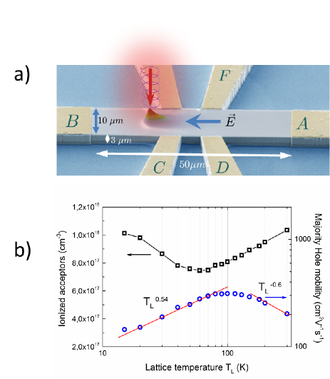
Here we experimentally measure in a 3 m thick, carbon doped p-GaAs active layer () and demonstrate the crucial role of the photoelectron temperature, in Eq. 1. The interface between the active layer and the S.I. GaAs substrate is a 50 nm thick GaInP epilayer that confines photoelectrons to the active layer and ensures that recombination at the interface is negligible. As shown in Fig. 1(a), a Hall bar is photolithographically etched into the active layer so that the lattice temperature () dependence of the majority hole concentration and mobility can be measured as shown in Fig. 1(b). The density of ionized acceptors is only weakly temperature dependent for this doping level since the impurity band and the valence band are merged into a continuum of states Kim et al. (1997); Lovejoy et al. (1995). The hole mobility at room temperature, , as well as its temperature dependence below 100 K are in good agreement with previous reports on similarly doped GaAs Colomb et al. (1992); Harmon et al. (1993); Lovejoy et al. (1995).
Spin-polarized photoelectrons were generated by a tightly-focussed circularly-polarized CW laser excitation (1/e half width of m, energy eV) in a setup described elsewhere Favorskiy et al. (2010). A maximum excitation power of 0.01 mW produces a non degenerate photoelectron concentration of in the steady state. was monitored from the high energy tail of the spatially homogenous luminescence spectrum, which is obtained using a multimode optical fiber placed in the image plane. As shown in Fig. 2(a), taken at a low electric field of V/cm, significantly differs from . Furthermore, Fig. 2(b) shows that without causing intervalley transitions Furuta et al. (1990); Okamoto et al. (2014), can be increased by applying higher electric fields. The lines in Fig. 2(b) are predictions based on a simple balance equation for the power delivered to the electron gas by the electric field. Here, is the electronic temperature at zero electric field, is the drift velocity and the energy relaxation time. The data is well explained by an energy independent energy relaxation time of ps and ps for initial electron temperatures of K and K, respectively. These values are an order of magnitude larger than values measured at K Furuta et al. (1990), consistent with a significant decrease of the energy relaxation rate at lower temperatures due to less efficient phonon scattering. Note that under similar electric fields, resistivity measurements in the dark show that the hole temperature () remains unchanged and that . This is not surprising since the photogenerated hole concentration is much smaller than .
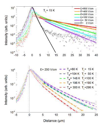
The minority carrier mobility is determined by imaging the spatial dependence of the luminescence, which is proportional to the electron concentration Favorskiy et al. (2010). Fig. 3 shows sections of these images along the direction of the electric field for 15 K (see movie attached as an ancillary file). Drift of the electrons in the applied electric field leads to a significant change of the profiles which are well approximated by the 2-dimensional diffusion result Luber et al. (2006)
| (2) |
where and are the electron diffusion constant and lifetime, respectively, and is a modified Bessel function of the second kind. In a nondegenerate electron gas the Einstein relation, , is valid so that the only fitting parameter in Eq. 2 is the product. An independent time resolved photoluminescence characterization of the sample was made in order to measure as a function of electron temperature Cadiz et al. (2014), so that a fit of Eq. 2 to the luminesence intensity profile yields an estimate for . At 300 K, , in excellent agreement with the theoretical value of at similar doping predicted by Bennett Bennett (2002) and with the existing experimental data Harmon et al. (1993); Colomb et al. (1992); Beyzavi et al. (1991); Ahrenkiel et al. (1987). The spin mobility was measured using a similar approach by placing a circularly-polarized excitation and a quarter wave plate followed by a linear polarizer at the reception, thus yielding the profile of the spin concentration , where is the concentration of electrons of spin , with a quantization axis along the direction of light excitation Favorskiy et al. (2010). The equation for is similar to Eq. 2 where and are replaced by their spin counterparts and . Using the predetermined value of the spin lifetime, Cadiz et al. (2014), an estimation of is possible.
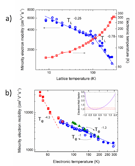
The results are summarized in Fig. 4. The charge and spin mobilities as a function of for a fixed electric field of 200 V/cm are shown in Fig. 4(a). It is first found that and equal within experimental error at all temperatures, thus verifying predictions for a nondegenerate electron gas in the absence of spin-dependent momentum relaxation mechanisms Qi et al. (2006). For K, varies as close to the behaviour previously reported in this temperature range Beyzavi et al. (1991). This exponent is reduced to -0.25 for 100 K. Fig. 4(a) also shows a linear variation of with above 100 K followed by a weaker variation at lower lattice temperatures.
The fixed field, variable mobility data are again plotted in Fig. 4(b) (full and open circles), this time as a function of . Above 100 K, a clear dependence is again observed, similar to that reported elsewhere Beyzavi et al. (1991). This suggests that what really determines minority carrier mobility is their own statistics, imposed by the light excitation energy and power, rather than that of majority carriers. This hypothesis can be tested by measuring the dependence of the mobilities when is varied by changing the electric field (see Fig. 2(b)) while is held constant. In this fixed , variable field measurement, the hole statistics do not change since . The results of this measurement are also shown in Fig. 4(b), the solid triangles corresponding to K and the solid squares corresponding to K. For 100 K 200 K the mobility dependence is well fitted by a law, close to that obtained in the fixed field, variable case (circles). For K there is a dramatic increase of mobility, with both electron and spin mobilities being described by a power law.
In order to determine separately the temperature dependences of the two factors in Eq. 1, can be measured using photoconductivity and photoHall measurements. Using a defocused laser excitation to ensure that the photoelectron concentration is homogeneous over the Hall bar, the ratio of the Hall mobility to the drift mobility of minority electrons can be found. can then be determined using Popovic (2004)
| (3) |
The result is at 15 K and at 300 K, in agreement with the values close to unity obtained for majority electrons in n-GaAsLook et al. (1996). Using these values and the graphical representation of Eq. 3 in the inset of Fig. 4(b), is found to lie between approximately -0.5 and 0.5, in qualitative agreement with the predictions of the Brooks-Herring model Chattopadhyay and Queisser (1981) for screened collisions by charged impurities. The small value of implies that the measured temperature dependences are mainly those of the prefactor in Eq. 1.
The origin of the dependence of the minority electron mobility is at present not understood. At the doping levels considered here it is probable that the mobility is determined by scattering off potential fluctuations caused by the random distribution of ionized acceptors and of their screening by valence holes. For 10 K the maximum amplitude of the potential fluctuations is of the order of 40 meV Efros et al. (1972) and while some attempts have been made to include the effects of screening on transport Kaneto et al. (1993); Chattopadhyay and Queisser (1981); Quang et al. (1993), a complete description including the effect of disorder is still out of reach. This work shows that in developing these models, accounting for the hole distribution alone Kaneto et al. (1993) cannot describe the observed temperature dependence of the minority electron mobility since significant variations are measured even when the hole temperature is constant. The inclusion of minority carrier statistics in theoretical models is therefore necessary to better understand minority carrier mobilities in doped semiconductors.
References
- Smith (1978) R. A. Smith, Semiconductors (Cambridge University Press, Cambridge, 1978).
- Beyzavi et al. (1991) K. Beyzavi, K. Lee, D. M. Kim, M. I. Nathan, K. Wrenner, and S. L. Wright, Appl. Phys. Lett 58, 1268 (1991).
- Luber et al. (2006) D. Luber, F. Bradley, N. Haegel, M. Talmadge, M. Coleman, and T. Boone, Appl. Phys. Lett 88, 163509 (2006).
- Schultes et al. (2013) F. Schultes, T. Christian, R. Jones-Albertus, E. Pickett, K. Alberi, B. Fluegel, T. Liu, P. Misra, A. Sukiasyan, H. Yuen, et al., Appl. Phys. Lett 103, 242106 (2013).
- Kim et al. (1997) S. Kim, C. Son, S. Chung, Y. Park, E. Kim, and S. Min, Thin Solid Films 310, 63 (1997).
- Lovejoy et al. (1995) M. L. Lovejoy, M. R. Melloch, and M. S. Lundstrom, Appl. Phys. Lett 67, 1101 (1995).
- Walukiewicz et al. (1979) W. Walukiewicz, J. Lagowki, L. Jastrzebski, and H. Gatos, J. Appl. Phys. 50, 5040 (1979).
- Kaneto et al. (1993) T. Kaneto, K. Kim, and M. Littlejohn, Phys. Rev. B 47, 16257 (1993).
- Colomb et al. (1992) C. M. Colomb, S. A. Stockman, S. Varadarajan, and G. E. Stillman, Appl. Phys. Lett 60, 65 (1992).
- Harmon et al. (1993) E. S. Harmon, M. L. Lovejoy, and M. R. Melloch, Appl. Phys. Lett 63, 536 (1993).
- Favorskiy et al. (2010) I. Favorskiy, D. Vu, E. Peytavit, S. Arscott, D. Paget, and A. C. H. Rowe, Rev. Sci. Instr. 81, 103902 (2010).
- Furuta et al. (1990) T. Furuta, H. Taniyama, and M. Tomizawa, J. Appl. Phys. 67, 293 (1990).
- Okamoto et al. (2014) N. Okamoto, H. Kurebayashi, T. Trypiniotis, I. Farrer, D. A. Ritchie, E. Saitoh, J. Sinova, J. Masek, T. Jungwirth, and C. H. W. Barnes, Nature Materials 13, 932 (2014).
- Cadiz et al. (2014) F. Cadiz, P. Barate, D. Paget, D. Grebenkov, J. P. Korb, A. C. H. Rowe, T. Amand, S. Arscott, and E. Peytavit, J. Appl. Phys. 116, 023711 (2014).
- Bennett (2002) H. S. Bennett, J. Appl. Phys. 92, 4475 (2002).
- Ahrenkiel et al. (1987) R. K. Ahrenkiel, D. J. Duniavy, D. Greenberg, H. C. Schlupmann, Hamaker, and H. F. MacMillan, Appl. Phys. Lett 51, 776 (1987).
- Qi et al. (2006) Y. Qi, Z. G. Yu, and M. E. Flatte, Phys. Rev. Lett 96, 026602 (2006).
- Popovic (2004) R. S. Popovic, Hall effect devices (Institute of Physics Publishing, Bristol, 2004).
- Look et al. (1996) D. Look, C. E. Stutz, J. R. Sizelove, and K. R. Evans, J. Appl. Phys. 80, 1913 (1996).
- Chattopadhyay and Queisser (1981) D. Chattopadhyay and H. J. Queisser, Rev. Mod. Phys. 53, 745 (1981).
- Efros et al. (1972) A. L. Efros, Y. S. Halpern, and B. I. Shklovsky, Proceedings of the International Conference on Physics of Semiconductors, Warsaw 1972 (Polish Scientific publishers, Warsaw, 1972).
- Quang et al. (1993) D. N. Quang, N. N. Dat, and D. V. An, Phys. Lett. A 182, 125 (1993).