Resonant transport and electrostatic effects in single molecule electrical junctions
Abstract
In this contribution we demonstrate structural control over a transport resonance in HS(CH2)n[1,4 - C6H4](CH2)nSH (n = 1, 3, 4, 6) metal |molecule |metal junctions, fabricated and tested using the scanning tunnelling microscopy-based method. The Breit-Wigner resonance originates from one of the arene -bonding orbitals, which sharpens and moves closer to the contact Fermi energy as increases. Varying the number of methylene groups thus leads to a very shallow decay of the conductance with the length of the molecule. We demonstrate that the electrical behaviour observed here can be straightforwardly rationalized by analyzing the effects caused by the electrostatic balance created at the metal-molecule interface. Such resonances offer future prospects in molecular electronics in terms of controlling charge transport over longer distances, and also in single molecule conductance switching if the resonances can be externally gated.
pacs:
73.63.Rt, 73.40.Sx, 85.65.+hI Introduction
The development of reliable techniques for the fabrication and electrical testing of metal |single molecule |metal junctions, supported by rapid developments in theoretical treatment of such junctions, has led to a significant re-invigoration of the wider field of ‘molecular electronics’.Nichols et al. (2010); Chen et al. (2007); Hybertsen et al. (2008); Chen and Tao (2009); Cuevas and Scheer (2010) The techniques used can be divided into two categories. One category uses solid-state electronics technology to fabricate so-called break junctions, in which a very thin metallic wire is deliberately broken (either by electromigration,Park et al. (2002) or by the application of mechanical stress Reichert et al. (2002)) in such a way that a molecule can bridge the resulting gap. The other category involves use of scanning probe microscopy to fabricate and characterise metal |molecule |metal junctions. For example, in the scanning tunnelling microscopy break junction (STM-BJ) method, a gold STM tip is driven into a gold substrate, and then retracted while the current is monitored. Xu and Tao (2003) As the resulting chains of gold atoms are broken, step decreases in the current approximately corresponding to the quantum of conductance, G0, are seen until the final chain of gold atoms is broken. In the presence of molecules that contain terminal potential binding groups (e.g. thiols Xu and Tao (2003), pyridines Xu and Tao (2003); Quek et al. (2009); Kamenetska et al. (2010), aminesChen et al. (2006); Venkataraman et al. (2006), carboxylate anions Chen et al. (2006); Martín et al. (2008), phosphinesPark et al. (2007); Parameswaran et al. (2010) , thioethersPark et al. (2007)), additional much smaller current step decreases are seen after the final gold atomic chain breaks, and these correspond to the subsequent breaking of metal |molecule |metal junctions. Alternatively, in the so-called (, current; , vertical height) method for measuring single molecule electricla properties, a gold STM tip is brought into close proximity of a surface coated with suitable molecules without allowing it to come into contact, and is then retracted while the tunnelling current is monitored. Haiss et al. (2003) When a molecule bridges the gap prior to tip retraction, a characteristic plateau is seen in the current-distance curve, prior to junction breakdown whereupon the current drops sharply.
For the great majority of (relatively short) molecules that have been studied in metal |single molecule |metal junctions, the mechanism of conductance has been found to be coherent tunnelling. Nichols et al. (2010) The conductance, GM, then varies as a function of the length of the bridging molecule according to Eq. (1):
| (1) |
where GG0TLTR (G0 is the quantum unit of conductance, 77.4 S, and TL and TR are the transmittances of the left hand and right hand connections of the molecule to the metal contacts; Gcon is called the contact conductance and represents the conductance of the system in the absence of the molecular backbone), R is the molecular backbone length and is the attenuation factor. A plot of lnGM vs. R is used to determine . Often, such molecules can be considered as “passive” molecular wires, in which the conductance decreases with bridge length in the simple manner predicted by phase coherent tunnelling. In many cases this length decay can be straightforwardly linked to the degree of conjugation, in turn related to the proximity of the relevant HOMO or LUMO (“frontier”) orbitals to the metal contact Fermi energies EF. However, molecular electronics is now aiming to achieve more active control over the electrical properties of molecular bridges. Approaches to this include electrochemical switching or conformational control of bridge structure and electronic states and control of quantum interference in molecular circuits.
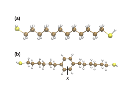
In earlier work, we showed that the conductance of junctions involving 6Ph6 and its derivatives (Fig. 1 ) was much higher (0.7 nS) than that measured for 1,12-dodecanedithiol (i.e. the two alkyl links for 6Ph6 connected back-to-back; 0.028 nSHaiss et al. (2009)), even though 6Ph6 (2.10 nm S…S distance) is considerably longer than 1,12-dodecanedithiol (1.72 nm S…S). We suggested that the reason for the unusually high conductance of 6Ph6 was that it behaves as a ‘molecular double tunnelling barrier’ in which a ‘well’ with lower HOMO-LUMO (-) separation is sandwiched between two ‘barriers’ with higher HOMO-LUMO (-) separation, by analogy with inorganic double tunnelling barrier structures involving III-V semiconductors.Leary et al. (2007) Clearly, the benzene moiety is capable of acting as an indentation in the tunnelling barrier. Interestingly, control over the conductance of the 6Ph6 family could be exerted chemically by using substituents on the aryl ring (Fig. 1); electron-donating substituents (Me, MeO) resulted in significantly higher junction conductances and the electron-deficient C6F4 group resulted in a lower conductance.Leary et al. (2007) Many studies of metal |molecule |metal junctions have probed the molecular structural requirements for obtaining high junction conductance.Ramachandran et al. (2003); Xu et al. (2005); Yamada et al. (2008); Lee et al. (2012); Dell et al. (2013); Sedghi et al. (2012, 2011, 2008); Li et al. (2012); Wang et al. (2009)
The work described in this contribution is aimed at a deeper understanding of the evolution of the orbital alignment in single-molecule junctions. To this end, we have investigated the effect of varying the width of the ‘barriers’ (i.e. the number of methylene groups) while keeping the ‘well’ (the 1,4C6H4 moiety) constant. Accordingly, we have now synthesised new molecules and have determined the single molecule conductances of 1,4HS(CH2)xC6H4(CH2)xSH (xPhx; x = 1, 3, 4, 6) using the technique, and we have carried out transport calculations on the molecules. We find that the variation of molecular conductance with in this family is surprisingly small, and that this is the consequence of the presence of a Breit-Wigner resonance in the transmission curve (caused by the higher-energy of the two - bonding orbitals of the benzene ring). This resonance sharpens and moves closer to the contact Fermi energy as increases, offsetting to some degree the rapid exponential decrease in conductance with length that might be expected for increasing . Thus, control over the conductance of these molecules can be exerted not only by substituents on the phenyl ring, but also by varying the alkyl chain length. More importantly, we show that this system can be understood in terms of a simple pair of back-to-back metal-semiconductor junctions where the alignment of the states in the internal part of the semiconductor primarily depends on how the electrostatic balance is established at the contact region. Such a balance is in turn mainly determined between the molecular mid-gap states and the metal Fermi level via charge transfer, which finally determines the position of the bulk resonance with respect to the Fermi level. We also show that investigating this system within this perspective is essential to understand the level alignment in the junction, which otherwise could not be fully explained by the initial trend in the gas phase.
II Experimental RESULTS
II.1 Syntheses, sample preparation and monolayer formation
1Ph1 (as the free di-thiol) is commercially-available and was used as received. 6Ph6 (di–thioacetate; Fig. 1) was synthesised as previously described Leary et al. (2007) and the same general approach was used to synthesise 3Ph3 and 4Ph4 ; full details are provided in the Supplemental Material (SM) SM . Gold-coated glass substrates (Arrandee) of ca. 1 x 1 cm size were flame-annealed using a butane-air torch to red heat, to generate Au(111) terraces, Haiss et al. (1991) as confirmed by STM imaging (see SM SM , Fig.1). The slides were allowed to cool, and were then immersed in a 10-3 M solution of the appropriate di-thioacetate (3Ph3, 4Ph4, 6Ph6) or dithiol (1Ph1) in CH2Cl2 for 1-2 minutes (1Ph1; 3 minutes) to afford a partial monolayer coverage of adsorbed dithiol molecules. Polarisation modulated infrared reflection-absorption spectroscopy (PM-IRRAS) was used to confirm that the adsorption of the molecules took place (for an example, see Fig.2 in the SM), and STM imaging of these submonolayers showed bright spots indicative of the presence of molecule(s), particularly at step edges (see SM SM , Fig.1c); molecular resolution could not be obtained, as is typical for highly-mobile adsorbed thiols at submonolayer coverages.
II.2 Single molecule conductance determination
The scanning tunnelling microscopy-based technique was used to determine single molecule conductance values for 1Ph1, 3Ph3, 4Ph4 and 6Ph6. In this technique, tip-substrate contact is avoided. A freshly-cut Au STM tip was brought into close proximity to the modified substrate surface using the appropriate set point current, and the tip was then retracted while the tunnelling current was measured. When a molecule (or molecules) bridge between tip and substrate, characteristic current plateaux in the current-vertical distance () traces result, and the molecular conductance is determined from a histogram of many such traces. In this work, at least 500 traces showing current plateaux (defined as having length 0.5 nm) were combined into conductance histograms for any given experiment; typically, approximately 15 of traces showed a plateau. Of the remaining traces, approximately 60 were straightforward exponential decays with no evidence of molecular bridge formation and the rest were noisy and showed no obvious plateau; traces in these categories were rejected. Two-dimensional histograms of conductance-vertical distance correlation were also constructed. The tip bias in all experiments was +0.6 V.
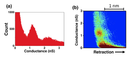
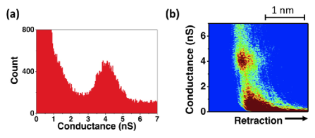
Initially, we began by repeating the experiment of Leary et al.Leary et al. (2007) using 6Ph6, with a set point current of 6 nA. This produced a relatively sharp histogram peak at a conductance of 0.82 0.18 nS, in good agreement with the results reported by Leary et al (see SM SM ; Fig.4). A second clear peak can also be seen at approximately twice this value, corresponding to junctions formed with two molecules in the gap. Next, we examined 4Ph4, 3Ph3 and 1Ph1. It was necessary to increase the set point current for these molecules, to 10, 20 and 30 nA respectively, since the molecules are progressively shorter, hence the tip has to be brought into closer proximity to the surface to ensure a reasonable percentage of successful junction formation events on tip retraction. Fig. 2 shows the results obtained for 4Ph4, and Fig. 3 those for 1Ph1; corresponding results for 3Ph3 are shown in Fig.3 in the SM SM . A small proportion of the traces from these experiments showed some evidence of a final, lower-conductance plateau, following the plateau that gave rise to the above conductance peaks. This suggested that lower-conductance junctions might form with these molecules at larger tip-substrate distances, but these plateaux do not give rise to a discernable separate conductance peak in either one-dimensional or two-dimensional histograms (see e.g. Fig. 2(a) and 2(b) where they are lost in the low-current noise at 0.8 nS). These events were quite rare, even when the set-point current was set to a smaller value to favour the formation of these longer, lower conductance plateaus over the shorter, higher conductance events, and so we did not analyse these events further. The data for all experiments are compared in Table 1. We used a previously-published procedure to measure the break-off distance (the distance z at which the junctions break down)Sedghi et al. (2008) and to correct this for the initial set-point distance z0 (the initial height of the STM tip). These break-off distances were similarly plotted as histograms (see SM SM , Fig.6). Since, as is evident from Fig. 2 and 3, the conductances of the junctions are rather invariant with distance for these highly flexible molecules, we use the 95th percentile break-off distance as an estimate of the maximum length of the junction at breakdown, and it can be seen from Table 1 that this correlates well with the theoretical length of a junction between the two contacting gold atoms, approximated for the fully-extended molecular conformation using molecular mechanics (Spartan 14). The exception is 1Ph1, where the junctions at breakdown are somewhat longer than expected for a molecule of this length. It is possible that for a very short molecule, extension of the junction results in gold atoms being pulled out from the surface prior to junction breakdown.
| Molecule |
|
|
|
|||||||||
|---|---|---|---|---|---|---|---|---|---|---|---|---|
| 1Ph1 | 4.14 0.58 | 1.4 | 1.1 | |||||||||
| 3Ph3 | 2.01 0.32 | 1.8 | 1.7 | |||||||||
| 4Ph4 | 1.21 0.19 | 1.9 | 1.9 | |||||||||
| 6Ph6 | 0.82 0.18 | 2.5 | 2.3 |
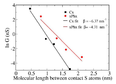
It is interesting to note that, alone of the molecules studied here, 1Ph1 has previously been studied by the STM-BJ technique, and at 0.6 V bias voltage, the conductance measured was 80 nS.Xiao et al. (2004) It has previously been shown that the STM-BJ method favours the formation of high conductance molecular junctions, and this has been interpreted in terms of the contact atoms binding to gold at step edges or similar defects, producing a junction with a shorter metal — metal distance and with additional channels for conduction through the molecule due to the step edge gold atom in close proximity to the molecular backbone.Haiss et al. (2009) In Fig. 4, we compare the conductance as a function of length between the sulfur contact atoms (calculated for the fully-extended molecules using the molecular mechanics approach in Spartan14) for the xPhx series with recent data for the alkanedithiols, measured in UHV.Pires et al. (2013) A notable feature of the conductance data for the xPhx series is the very low apparent value of (calculated from the slopes of these lines; Eq. (1)), 1.52 nm-1.
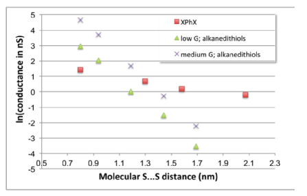
Since the only structural change in the molecules xPhx is the length of the alkyl chains, it is pertinent to compare the values with those found for alkanedithiols in related STM-based experiments; reported values range from 7-8.2 nm-1 for all three conductance groups.Haiss et al. (2009); Li et al. (2007); Busiakiewicz et al. (2010) Since the Fermi energy of the contacts has to fall between the HOMO and LUMO of the molecule in the junction, for molecules conducting via a tunnelling mechanism one expects the value to depend upon the HOMO-LUMO separation, with more conjugated molecules having a smaller HOMO-LUMO gap and hence a smaller . For instance, for a series of oligophenyl methanethiols (C6H5CH2SH, C6H5C6H4CH2SH and C6H5C6H4C6H4CH2SH), was determined as 4.6 0.7 nm-1 using the GaIn/Ga2O3 eutectic contact technique on self-assembled monolayers of the molecules on template-stripped gold electrodes Fracasso et al. (2013) (a similar value, 4.2 0.7 nm-1, was determined earlier using a conducting AFM techniqueWold et al. (2002)), while for a series of oligothiophenes with 5, 8, 11 and 14 2,5-coupled thiophene rings, was 1 nm-1, measured by the STM break junction method.Yamada et al. (2008) The lowest values so far measured have been for extended viologens (0.06 nm-1) Kolivoska et al. (2013) and for conjugated fused oligoporphyrins, oligoporphyrin-ethynylene and oligoporphyrin–butadiynylene systems, where values of 0.2 to 0.4 nm-1 have been found, the exact value depending on structure.Sedghi et al. (2012, 2011, 2008); Li et al. (2012) It should be noted that although a low value of is often taken as an indication that the conductance mechanism could be hopping rather than superexchange (tunnelling), it has been shown that the conductance behaviour of even the most conjugated of these families of porphyrins as a function of temperature are still described well by theoretical models involving tunnelling.Sedghi et al. (2012) In this context, a value of of ca. 1.5 nm-1 is remarkably small for the xPhx series, given that the only variable in this series is the number of methylene groups, for which we would expect to be 7-8 nm-1. To check for a possible hopping mechanism, we have carried out conductance measurements as a function of temperature on a representative molecule from this series, 6Ph6 (for data, see Fig.5 in the SM SM ). The conductance of this molecule as determined by the technique did not vary, within experimental limits, over the temperature range 20-100 ∘C. This confirms that a hopping mechanism is not operative, as expected since a single benzene ring is not redox-active within conventional potential limits.
III Theoretical modelling and discussion
To gain insight into the conductance behavior of the xPhx system we performed DFT and electronic transport calculations with the help of the code GaussianFrish et al. (2003) , using the PBE functionalPerdew et al. (1997) and the LANL2DZ basis set,Wadt and Hay (1985) unless otherwise specified. The molecular junctions were built by matching the S atoms of the molecule with the S atoms of the S-Au structure. The electronic transport calculations were carried out with ANT.G,Palacios et al. ; Jacob and Palacios (2011) which is built as an interface to Gaussian. This code computes the electronic transmission using non-equilibrium Green’s function techniques in the spirit of the Landauer formalism, employing parametrized tight-binding Bethe lattices in the far electrode description. Jacob and Palacios (2011) A CRENBS basis set was usedRoss et al. (1990) for the Au atoms in the outermost layers. Further details of the calculations involving alternative contact sites (top, step) are given in the SM SM . We optimized the molecular structures for the geometries of 1Ph1, 3Ph3, 4Ph4 and 6Ph6 in the gas phase and then relaxed a S atom on top of a 19 gold atom cluster (together with the gold atoms in the top layer). Then we analyzed their electronic structure after removing the terminal H atoms, which are known to be lost upon adsorption onto gold under our conditions.Love et al. (2005)
For all molecules, the HOMO-2 is localized on the benzene ring and is found to rise in energy as the chain length increases (see Fig. 9). As will be seen later in the discussion, the length dependence of the alignment of this orbital with the Fermi energy plays a determining role in the conductance behavior. The LUMO, HOMO and HOMO-1 all consist of spin degenerate levels, localized on the S atoms. Orbitals localized on the alkyl chains are far below in energy. In the left panel of Fig. 5, we show the orbitals for the longest molecule (6Ph6) with the corresponding energies. It can be observed that the LUMO (localized on the S atoms) is quite close in energy to the HOMO, while the LUMO+1 (localized on the benzene) is far above. More importantly, a clear spatial separation appears between the states localized on the S atoms and those localized on the benzene ring.
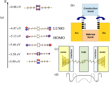
In our view, the LUMO+1 and HOMO-2 can be likened to the conduction-valence band structure in a semiconductor, while the states in between (LUMO, HOMO and HOMO-1) can be likened to the surface midgap states of the semiconductor as they are mainly localized on the S atoms that connect to the electrodes. Consequently, placing this molecule between two metal electrodes will form a junction that is expected to behave like a pair of back-to-back metal-semiconductor junctions in which the chemical terminations of the semiconductor create states within its band gap (as schematically depicted in Fig. 5b). For the purposes of this analogy we refer to the benzene core of the molecule as the “semiconductor bulk”. The whole junction can then be thought of as divided into five main blocks: metal-interface-bulk-interface-metal (Fig. 5c). Each diode consists of a metal-(organic) semiconductor point-like junction. In our case, the semiconductor is intrinsic and the metal Fermi level falls between the HOMO and the LUMO of the central benzene ring (i.e. between the HOMO-2 and the LUMO+1 of the complete system).
It is not straightforward, a priori, to know where the Fermi level will lie in this gap. However, insights can be gained by considering what happens at the interface between a metal and a semiconductor. In analogy with the semiconductor surface states, the states localized on the S atoms of the xPhx molecules should be strongly hybridized when interacting with the metal, giving rise to the so-called ‘gateway states’Widawsky et al. (2013). The mismatch between the metal Fermi level and the molecular charge neutrality level (CNL) at the interface induces a charge transfer which in turn creates a point-like dipole;Flores et al. (2009) the energy levels in the inner part of the semiconductor bulk are then shifted up or down due to the dipole by a quantity which varies with the distance from the interface (Fig. 5d). The role of dipole interfaces has been extensively investigated in the case of organic monolayers or (more generally) single molecules lying flat on surfaces Heimel et al. (2006); Bokdam et al. (2011); Hofmann et al. (2010); Braun et al. (2009) but, to the best of our knowledge, a thorough study concerning their roles in junctions comprising a single molecular nanowire held between two metal clusters has not been explored to the same extent.Gutiérrez et al. (2003); Xue et al. (2001); Peng et al. (2009) It is worth stressing that in this case, since the semiconductor is intrinsic, no depletion layer is formed. Consequently, variations in the energy position of the bulk levels must not be ascribed to the typical band bending associated with it in doped semiconductors. Here, the only electrostatic effect is related with the dipole established at the interface and will be confined to a narrow region close to it. Notice also that while in a planar junction the bands are shifted at (infinitely) large distances,Léonard and Tersoff (2000) in a single-point junction, such as the one considered here, the effect of the dipole effect is expected to decay rapidly along the transport direction. In what follows, we proceed to analyze the energetics of the four molecules when placed between two gold electrodes; we will show how studying the electrostatic balance established at the metal-molecule interface is essential for a thorough understanding of the level alignment, which in turn impacts on charge transport across the junction.
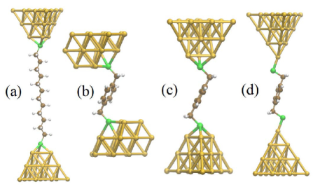
We constructed junctions in which each molecule is connected to two gold clusters, in the hollow, top or step binding geometry (see Fig. 6); however, in what follows, we will restrict discussion to the hollow position. For comparison, we also studied a series of alkanedithiols of four different lengths (C2, C6, C8 and C12), also bound in the hollow position. Although their total lengths are different from the xPhx molecules, this comparison was made to give insight into the presence of any additional state(s) and into differences in the length dependence. In Fig. 7, we show the low-bias transmission curves obtained for the Cx and xPhx series in the hollow geometry. For the xPhx molecules, the presence of additional peaks is evident. These Breit-Wigner resonances approach the Fermi level as the molecular length increases (consistent with previous calculations Hüser (2009); Benesch et al. (2008)) and they do not appear in the case of the Cx molecules. The presence of these states creates an indentation in the barrier, confirming our earlier suggestion Leary et al. (2007). A similar effect has previously been shown in another system.Zotti et al. (2013) These resonances stem from the HOMO-2, which is localized on the benzene ring, thus they become narrower as the increasing benzene-gold distance decouples them from the gold contacts. To some extent, the benzene ring behaves as a quantum dot, weakly coupled to the electrodes by the alkyl chains. The trend in energy of the peaks approximately follows that in the gas phase for 3Ph3, 4Ph4, and 6Ph6, whereas the corresponding peak of 1Ph1 lines up further down in energy (at -1.48 eV). Indeed, in the case of this shorter molecule, exceptional behavior is expected due to the strong hybridization of the orbitals. In the case of the Cx molecules, the states closest to the Fermi level are localized mainly on the S atoms, while states localized on the whole chain appear only below -2 eV.
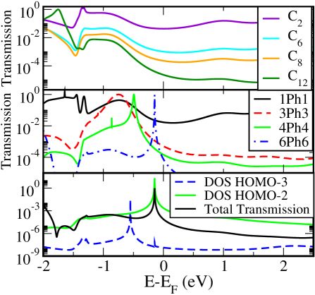
To discern the different contributions in the transmission curves of the xPhx molecules, we calculated the DOS projected onto the molecular orbitals. The results are illustrated for 6Ph6 in the lowest panel of Fig. 7. These projections clearly show that the sharp peak visible in the transmission curve close to the Fermi level for 6Ph6 is due to the HOMO-2, while the HOMO-3, also mainly localised on the benzene ring, does not yield any peak in the transmission curve apart from a very small Fano resonance (interference effects in transport through benzene rings have been widely studied Darau et al. (2009)). The broad bumps at around -1 eV derive from the gateway states, i.e. from the hybridization of S-Au states at the interface. Notice that using the same voltage 0.6 V as in the experiments is not expected to change the overall picture. To confirm this, we show, in the SM, a comparison between the transmission curves for 4Ph4 calculated at 0 and 0.6 V: the position of the HOMO-2 is not affected, while the bias voltage seems to rather have an influence on the interface states.
We now turn to analyse these systems quantitatively. In what follows, we will focus on the metal-molecule interface of our system in order to discern the various contributions that determine the level alignment in the studied junctions. We again focus on the hollow binding geometry. To begin with, we have first analyzed the Mulliken charges in order to discern whether any significant charge transfer takes place in this system (see Table I in the SM SM ). They show an increased electron charge (around 0.3) on each gold cluster and corresponding positive charge on the outermost carbon atoms, indicating charge transfer from the molecule onto the metal. Subsequently, we have analysed a system consisting of each molecule connected to a single Au19 cluster in a hollow position, with the aim of understanding the level alignment at just one metal-molecule interface. In this case, as well as the standard DFT calculation, we have also performed constrained DFT (c-DFT) calculations, as explained below. By connecting a Bethe lattice to the metal cluster, a new system is built, where the molecule is now connected to a semi-infinite electrode (see Ref. Jacob and Palacios, 2011 for more details). The system can be hence divided into two parts, namely the lead and the main region that comprises the molecule and a certain number of metal layers. The density matrix of this region is calculated as
| (2) |
where the retarded Green’s function is given by
| (3) |
Here, is the Hamiltonian of the main region, is the lead self energy, which describes the coupling to the semi-infinite lead, and is a quantity by which the on-site energies of the Hamiltonian must be shifted in order to ensure the total-charge neutrality ( is opposite in sign to the chemical potential). In our c-DFT any charge transfer between the two parts is forbidden. Both surface and molecule were forced to keep a number of electrons as to maintain charge neutrality. To this aim, was computed in alternation so as to meet the imposed charge constraints on the metal and the molecule. If and are the desired number of electrons in the surface and the molecule, respectively, then two different chemical potentials and are calculated so that
| (4) |
| (5) |
where and are the number of atomic orbitals of the surface and the molecule, respectively. At each iteration step the density matrix is then built as a block matrix as follows:
| (6) |
The off-diagonal terms in the submatrices were set to zero. The so-built density matrix is out of equilibrium, with two different chemical potentials in the metal and the molecule (at approximately -5.96 eV and -4.2 eV for metal and molecule, respectively), consequently giving rise to a step potential across the system. The Fermi level of the molecule calculated in this way can be interpreted as the charge neutrality level (CNL) discussed in the literature, Flores et al. (2009); Vázquez et al. (2005) but obtained in a more rigorous way. It defines the direction in which electronic charge is most likely to be transferred. In our case, the CNL is definitely higher than the Au Fermi level, so charge transfer from the molecule onto the metal is expected, confirming what was indicated by the Mulliken charges in the junction.
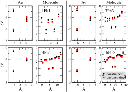
We now turn to analyze what happens once the electronic charge has been transferred. To this end, we have computed the on-site energies along the Au19-molecule junctions and compared them with those resulting from the constrained calculation (the results are shown in Fig. 8). They were evaluated as the average (over the atomic orbitals of each atom) of the diagonal terms in the Kohn-Sham Hamiltonian. Since the absolute values along the vertical axes are not physically relevant, as they are strongly related to the basis-set choice for each atom, they have been offset for clarity. Hence, we will only focus on the comparison between the values obtained in two kinds of calculations. At the interface, we see a clear sign of the expected dipole; in the unconstrained calculation the values are shifted upwards in the metal and downwards in the molecule. In the latter, the effect is stronger in the carbon atoms closer to the metal, fading away as the distance from the metal increases. In 1Ph1, the shortest molecule, the benzene ring is quite close to the gold and shows some positive charge (0.1) in the unconstrained calculation, as compared to that constrained. Indeed, for 1Ph1 the on-site energies are strongly affected also in the C atoms of the benzene ring. It is also worth adding that, when a second cluster is added at the other end of the molecules to complete the junctions, the effects caused by the dipole in the bulk region are expected to increase. The Mulliken charges along the Au19-molecule junctions in the constrained and unconstrained calculations are shown in the SM.SM
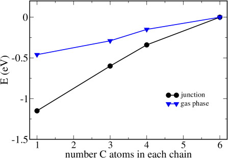
We summarize all these results as follows: when the xPhx molecules approach the metal, Fermi-level alignment is achieved upon charge transfer from the sulfur, or the outermost carbon atoms, onto the metal. This generates a dipole potential mainly near the interface. The molecular bulk states (HOMO-2 levels) then behave like spectators, with their energetic positions being dragged down under the influence of the dipole potential according to the distance from the interface (Fig. 5d), and never crossing the Fermi level (see, for example, the case of the top binding geometry for the hypothetical 8Ph8 in the SM SM ). The level alignment of the bulk states is governed purely by electrostatics because of the clear separation from the interface (apart from 1Ph1) as already discussed. Note that this would not be possible in fully conjugated molecules, where other effects such as hybridization would also play a role. Notice that any electrostatic-induced shift is added to the one the HOMO-2 already presents in the gas phase for increasing chain length (see, in Fig. 9, a comparison between the energy shift experienced by this orbital in the gas phase and in the junction).
It should be recalled that there is some uncertainty in the position of the HOMO-2 peak in the transmission curves as it corresponds to a Kohn-Sham state, and it might be located at lower energies. Nevertheless, the computed transmission curves provide an insight into the alignment dynamics, i.e. they clearly show how the alignment of the bulk states is governed by the gas-phase behavior, modulated by what happens at the interface. To support our interpretation of the numerical results, it is important to verify that the benzene ring falls inside the space region in which the dipole-potential effect is confined. To this aim, we have calculated the potential generated in the middle of the benzene ring by the charges at the interface. The results are reported in Table II of SM SM and show decreasing values for increasing chain length, with maximum values of around 1 eV.
Overall, the scenario described above provides a good rationalisation for the experimentally observed low value of . There are two counteracting effects, namely the expected decay due to increasing molecular length on the one hand, together with the increasing sharpness of the HOMO-2 resonance in the molecules with longer polymethylene bridges, and the approach to the Fermi energy of the resonance peak on the other hand. Fig. 10 shows a plot of calculated zero bias conductance vs. molecular length for the xPhx and Cx molecules. Although the absolute values of the conductances differ substantially from the experimentally observed values, it can be clearly seen that the calculated value is smaller for the xPhx series than for the Cx molecules, although the factor by which they differ (ca. 1.5) is substantially smaller than that seen experimentally (ca. 4.8). Nevertheless, given the known problems with DFT, and the limitations inherent in the modeling of the contacts, we believe that this offers a good explanation for the experimental observations. Ultimately, possible asymmetries in the experimental junctions should be taken into account (not considered here) which lead to transmission resonances with a maximum height lower than 1. While this is not expected to change the conductance values for the Cx molecules, for which the resonances show up further below the Fermi energy, it might change the conductance values for the xPhx molecules and, consequently, the factor.
IV CONCLUSIONS
We studied the series of molecules HS(CH2)x[1,4–C6H4](CH2)xSH (x = 1, 3, 4, 6) and found that the rate of conductance decay with molecular length is smaller than that measured previously for alkanedithiols. This was found to be due to the decreasing distance in energy of the Breit-Wigner resonance from the Fermi level for increasing molecular length. This trend originates from the orbital behaviour in the gas phase but is modulated by the electrostatic balance established at the electrode contact region.
V Acknowledgments
This research was supported by the EPSRC (Grant No. EP/H035184/1), by MINECO under Grant No. FIS2013-47328, by the European Union structural funds and the Comunidad de Madrid MAD2D-CM Program under Grant. P2013/MIT-2850, and by Generalitat Valenciana under Grant PROMETEO/2012/011. We thank M. Soriano for help with the computational part and acknowledge the computer resources, technical expertise, and assistance provided by the Centro de Computacion Cientifica of the Universidad Autonoma de Madrid.
References
- Nichols et al. (2010) R. J. Nichols, W. Haiss, S. J. Higgins, E. Leary, S. Martin, and D. Bethell, Physical Chemistry Chemical Physics 12, 2801 (2010).
- Chen et al. (2007) F. Chen, J. Hihath, Z. Huang, X. Li, and N. Tao, Annu. Rev. Phys. Chem. 58, 535 (2007).
- Hybertsen et al. (2008) M. S. Hybertsen, L. Venkataraman, J. E. Klare, A. C. Whalley, M. L. Steigerwald, and C. Nuckolls, Journal of Physics: Condensed Matter 20, 374115 (2008).
- Chen and Tao (2009) F. Chen and N. Tao, Accounts of Chemical Research 42, 429 (2009).
- Cuevas and Scheer (2010) J. C. Cuevas and E. Scheer, Molecular electronics: an introduction to theory and experiment (World Scientific,Singapore, 2010).
- Park et al. (2002) J. Park, A. N. Pasupathy, J. I. Goldsmith, C. Chang, Y. Yaish, J. R. Petta, M. Rinkoski, J. P. Sethna, H. D. Abruña, P. L. McEuen, et al., Nature 417, 722 (2002).
- Reichert et al. (2002) J. Reichert, R. Ochs, D. Beckmann, H. Weber, M. Mayor, and H. von Löhneysen, Phys. Rev. Lett 88, 176804 (2002).
- Xu and Tao (2003) B. Xu and N. J. Tao, Science 301, 1221 (2003).
- Quek et al. (2009) S. Y. Quek, M. Kamenetska, M. L. Steigerwald, H. J. Choi, S. G. Louie, M. S. Hybertsen, J. Neaton, and L. Venkataraman, Nature Nanotechnology 4, 230 (2009).
- Kamenetska et al. (2010) M. Kamenetska, S. Y. Quek, A. Whalley, M. Steigerwald, H. Choi, S. G. Louie, C. Nuckolls, M. Hybertsen, J. Neaton, and L. Venkataraman, Journal of the American Chemical Society 132, 6817 (2010).
- Chen et al. (2006) F. Chen, X. Li, J. Hihath, Z. Huang, and N. Tao, Journal of the American Chemical Society 128, 15874 (2006).
- Venkataraman et al. (2006) L. Venkataraman, J. E. Klare, I. W. Tam, C. Nuckolls, M. S. Hybertsen, and M. L. Steigerwald, Nano Letters 6, 458 (2006).
- Martín et al. (2008) S. Martín, W. Haiss, S. Higgins, P. Cea, M. C. Lopez, and R. J. Nichols, The Journal of Physical Chemistry C 112, 3941 (2008).
- Park et al. (2007) Y. S. Park, A. C. Whalley, M. Kamenetska, M. L. Steigerwald, M. S. Hybertsen, C. Nuckolls, and L. Venkataraman, Journal of the American Chemical Society 129, 15768 (2007).
- Parameswaran et al. (2010) R. Parameswaran, J. Widawsky, H. Vazquez, Y. Park, B. Boardman, C. Nuckolls, M. Steigerwald, M. Hybertsen, and L. Venkataraman, The Journal of Physical Chemistry Letters 1, 2114 (2010).
- Haiss et al. (2003) W. Haiss, H. van Zalinge, S. J. Higgins, D. Bethell, H. Höbenreich, D. J. Schiffrin, and R. J. Nichols, Journal of the American Chemical Society 125, 15294 (2003).
- Haiss et al. (2009) W. Haiss, S. Martín, E. Leary, H. v. Zalinge, S. J. Higgins, L. Bouffier, and R. J. Nichols, The Journal of Physical Chemistry C 113, 5823 (2009).
- Leary et al. (2007) E. Leary, S. J. Higgins, H. van Zalinge, W. Haiss, and R. J. Nichols, Chem. Commun. , 3939 (2007).
- Ramachandran et al. (2003) G. K. Ramachandran, J. K. Tomfohr, J. Li, O. F. Sankey, X. Zarate, A. Primak, Y. Terazono, T. A. Moore, A. L. Moore, D. Gust, et al., The Journal of Physical Chemistry B 107, 6162 (2003).
- Xu et al. (2005) B. Q. Xu, X. L. Li, X. Y. Xiao, H. Sakaguchi, and N. J. Tao, Nano Letters 5, 1491 (2005).
- Yamada et al. (2008) R. Yamada, H. Kumazawa, T. Noutoshi, S. Tanaka, and H. Tada, Nano letters 8, 1237 (2008).
- Lee et al. (2012) S. K. Lee, R. Yamada, S. Tanaka, G. S. Chang, Y. Asai, and H. Tada, ACS Nano 6, 5078 (2012).
- Dell et al. (2013) E. J. Dell, B. Capozzi, K. H. DuBay, T. C. Berkelbach, J. R. Moreno, D. R. Reichman, L. Venkataraman, and L. M. Campos, Journal of the American Chemical Society 135, 11724 (2013).
- Sedghi et al. (2012) G. Sedghi, L. J. Esdaile, H. L. Anderson, S. Martin, D. Bethell, S. J. Higgins, and R. J. Nichols, Advanced Materials 24, 653 (2012).
- Sedghi et al. (2011) G. Sedghi, V. M. García-Suárez, L. J. Esdaile, H. L. Anderson, C. J. Lambert, S. Martín, D. Bethell, S. J. Higgins, M. Elliott, N. Bennett, et al., Nature Nanotechnology 6, 517 (2011).
- Sedghi et al. (2008) G. Sedghi, K. Sawada, L. J. Esdaile, M. Hoffmann, H. L. Anderson, D. Bethell, W. Haiss, S. J. Higgins, and R. J. Nichols, Journal of the American Chemical Society 130, 8582 (2008).
- Li et al. (2012) Z. Li, T.-H. Park, J. Rawson, M. J. Therien, and E. Borguet, Nano Letters 12, 2722 (2012).
- Wang et al. (2009) C. Wang, A. S. Batsanov, M. R. Bryce, S. Martín, R. J. Nichols, S. J. Higgins, V. M. García-Suárez, and C. J. Lambert, Journal of the American Chemical Society 131, 15647 (2009).
- (29) “See supplemental material at [url will be inserted by publisher] for details about synthetic procedures, single molecule experiments, theoretical calculations and spectra of compounds,” .
- Haiss et al. (1991) W. Haiss, D. Lackey, J. K. Sass, and K. H. Besocke, The Journal of Chemical Physics 95, 2193 (1991).
- Xiao et al. (2004) X. Xiao, B. Xu, and N. J. Tao, Nano Letters 4, 267 (2004).
- Pires et al. (2013) E. Pires, J. E. Macdonald, and M. Elliott, Nanoscale 5, 9397 (2013).
- Li et al. (2007) Z. Li, I. Pobelov, B. Han, T. Wandlowski, A. Błaszczyk, and M. Mayor, Nanotechnology 18, 044018 (2007).
- Busiakiewicz et al. (2010) A. Busiakiewicz, S. Karthäuser, M. Homberger, P. Kowalzik, R. Waser, and U. Simon, Physical Chemistry Chemical Physics 12, 10518 (2010).
- Fracasso et al. (2013) D. Fracasso, M. I. Muglali, M. Rohwerder, A. Terfort, and R. C. Chiechi, The Journal of Physical Chemistry C 117, 11367 (2013).
- Wold et al. (2002) D. J. Wold, R. Haag, M. A. Rampi, and C. D. Frisbie, The Journal of Physical Chemistry B 106, 2813 (2002).
- Kolivoska et al. (2013) V. Kolivoska, M. Valasek, M. Gal, R. Sokolova, J. Bulickova, L. Pospisil, G. Meszaros, and M. Hromadova, The Journal of Physical Chemistry Letters 4, 589 (2013).
- Frish et al. (2003) M. J. Frish, G. W. Trucks, and H. B. S. et al., GAUSSIAN 03, Revision B.01,Gaussian. Inc., Pittsburg (2003).
- Perdew et al. (1997) J. P. Perdew, K. Burke, and M. Ernzerhof, Phys. Rev. Lett 78, 1396 (1997).
- Wadt and Hay (1985) W. R. Wadt and P. J. Hay, The Journal of Chemical Physics 82, 284 (1985).
- (41) J. J. Palacios, D. Jacob, A. J. Perez-Jimenez, E. S. Fabian, E. Louis, and J. A. Verges, ALACANT ab initio quantum transport package, see URL: http://alacant.dfa.ua.es .
- Jacob and Palacios (2011) D. Jacob and J. J. Palacios, Journ. Chem. Phys. 134, 044118 (2011).
- Ross et al. (1990) R. Ross, J. Powers, T. Atashroo, W. Ermler, L. LaJohn, and P. Christiansen, The Journal of chemical physics 93, 6654 (1990).
- Love et al. (2005) J. C. Love, L. A. Estroff, J. K. Kriebel, R. G. Nuzzo, and G. M. Whitesides, Chemical Reviews 105, 1103 (2005).
- Widawsky et al. (2013) J. R. Widawsky, W. Chen, H. Vázquez, T. Kim, R. Breslow, M. S. Hybertsen, and L. Venkataraman, Nano Letters 13, 2889 (2013).
- Flores et al. (2009) F. Flores, J. Ortega, and H. Vázquez, in Advances in Solid State Physics (Springer, 2009) pp. 207–218.
- Heimel et al. (2006) G. Heimel, L. Romaner, J.-L. Brédas, and E. Zojer, Surface Science 600, 4548 (2006).
- Bokdam et al. (2011) M. Bokdam, D. Çakır, and G. Brocks, Applied Physics Letters 98, 113303 (2011).
- Hofmann et al. (2010) O. T. Hofmann, D. A. Egger, and E. Zojer, Nano letters 10, 4369 (2010).
- Braun et al. (2009) S. Braun, W. R. Salaneck, and M. Fahlman, Advanced Materials 21, 1450 (2009).
- Gutiérrez et al. (2003) R. Gutiérrez, G. Fagas, K. Richter, F. Grossmann, and R. Schmidt, EPL (Europhysics Letters) 62, 90 (2003).
- Xue et al. (2001) Y. Xue, S. Datta, and M. A. Ratner, The Journal of Chemical Physics 115, 4292 (2001).
- Peng et al. (2009) G. Peng, M. Strange, K. S. Thygesen, and M. Mavrikakis, The Journal of Physical Chemistry C 113, 20967 (2009).
- Léonard and Tersoff (2000) F. Léonard and J. Tersoff, Physical Review Letters 84, 4693 (2000).
- Hüser (2009) F. Hüser, Diploma Thesis, Universität Karlsruhe (2009).
- Benesch et al. (2008) C. Benesch, M. Cizek, J. Klimeš, I. Kondov, M. Thoss, and W. Domcke, The Journal of Physical Chemistry C 112, 9880 (2008).
- Zotti et al. (2013) L. A. Zotti, E. Leary, M. Soriano, J. C. Cuevas, and J. J. Palacios, Journal of the American Chemical Society 135, 2052 (2013).
- Darau et al. (2009) D. Darau, G. Begemann, A. Donarini, and M. Grifoni, Physical Review B 79, 235404 (2009).
- Vázquez et al. (2005) H. Vázquez, F. Flores, and A. Kahn, IPAP Conf. Series 6 , 1 (2005).