Study of the new superconducting compound Zr0.97V0.03B2 with point-contact spectroscopy.
Abstract
We present a study of the superconducting energy gap performed with point contact spectroscopy in a single crystal of the superconductor Zr0.97V0.03B2. We determined the size and evolution with temperature of the energy gap, the transition temperature in the compound occurs at the onset of T 9.3 K. The point contact junctions were measured from 1.7 to 20 K. The differential conductance as a function of bias voltage was analyzed with the Blonder-Tinkham-Klapwijk model, the evolution of the gap with temperature was compared with the BCS theory, the ratio 2(0)/KBTC was of the order of 8.95 indicative of a very strong coupling limit.
pacs:
74.70.Tx,74.80.Fp Superconductivity, Point Contact SpectroscopyI Introduction
In new superconductors one of the important parameters to be determined is the transition temperature and the emergence of the energy gap, among other parameters. On this respect many experimental tools actually exist to perform this determination. Perhaps some of the most direct tools are tunneling and point contacts spectroscopy (PCS). The first one, tunneling, was used in 1960 by I. Giaever to see and measure, for the first time the superconducting energy gap in Pb IvarG ; IvarGi . Later and because the many experimental troubles to prepare reliable tunnel junctions, as frequently observed by experimentalists wolf another spectroscopic technique quite similar to tunneling was used; point contact spectroscopy (PCS) developed by Sharvin Sharvin , and used posteriorly by Yanson to study electron phonon interaction in metals and superconductors I. K. Yanson . With this tool is simpler to build junctions and to perform studies to determinate parameters of superconductors as compared with tunneling. It is important to mention that PCS may provide the form to study mechanism of quasiparticles scattered by different interactions close to the Fermi surface. PCS junctions are able to extend the analysis provided by tunnel junctions to study electronic processes in single crystals, in different crystallographic directions and are both complementary techniques. PCS may be used in compounds where the construction of tunnel junction is difficult. PCS and tunneling junctions analysis mainly consist into measure the differential resistance as a function of the bias voltage and temperature of the material under study connected to another superconductor or to a normal electrode I. K. Yanson ; K.Yanson ; Yanson . Many forms and variety of techniques have been used to fabricate PCS; needle-anvil, I. K. Yanson , membranes with nano-holes Upadhyay , mechanical breaking junctions Muller .
In this work the manner used for fabricating PCS consist of using a fine thin wire to contact an edge or surface of the superconducting sample. The tip of the normal fine wire is used to inject electrons to the superconducting sample. This procedure was described by Escudero et al. Escudero . To obtain reliable spectroscopic information of the electronic parameters of the superconductor the operating conditions for the PCS are quite strict classified into three different regimes of conduction: ballistic, thermal, and diffuse, established with the parameters associated to the material under study and to the geometry of the contact these are; the electronic mean free path () and the contact radius () Daghero ; Sharvin ; Duif ; Jansen ; Wexler .
For the analysis of the data measured with the PCS various theoretical models are used, the simplest one is the BTK model (Blonder,Tinkham and Klapwijk)Blonder . This one describes the electronic transport through a constriction formed by a normal metal and a superconductor, operating in the ballistic regime. The model includes the effects caused by incorporating an insulating barrier at the interface, the barrier allows to modeling the limits from metallic contact to tunneling junction by varying a parameter denoted as , the dimensionless barrier strength Blonder . Other theoretical models based in BTK include the degree of polarization in magnetic junctions and can be used for further analysis Strijkers . With BTK model is possible to determine the properties of the material under study i.e, the size of the energy gap, , its evolution with temperature, etc. The PCS measurements may give information related to the density of electronic states, mechanisms of electronic scattering in metals i.e, phonons, charge density wave, spin density, etc. Its application to the superconducting state provides direct information on the electron-phonon interaction, responsible for the formation of the electronic coupling Michael ; Terry ; Jansen ; Kedves ; Raymond .
In this work we focus on the study of the induced superconductivity in ZrB2 by replacing Zr by small quantities of Vanadium. The highest transition temperature obtained at date was T 9.3 K, obtained with a substitution of 3 to 4% of Vanadium following a procedure similar to the described by I. K. Yanson ; V. A. Gasparov ; Gasparov ; Soon ; Renosto ; J. Wang . Our resulting composition was Zr0.97V0.03B2. PCS results were obtained with junctions formed with a thin wire of tungsten plated gold of 5 m diameter, W(Au), and a superconducting single crystal. This study is mainly focused into the determination and evolution with temperature of the superconducting energy gap analyzed using the BTK model. At K the relationship 2 suggests a superconductor in the strong coupling limit.
II Experimental Details
II.1 Crystal Data
Single crystals of Zr0.97V0.03B2 were obtained by mixing high purity elements and melted in a tri-arc furnace with Cu cold cathode in a inert atmosphere of Ar-H2 at 5% H2. Several stoichiometries Zr1-xVxB2 were formed with values of x = 0.02, 0.04, and 0.08. Excess boron, about 10% was introduced in order to provide the desired stoichiometry. The resulting final composition was processed several times in order to have a homogeneous composition. At the final process it was annealed at high temperatures in evacuated quartz tubes. The resulting were single small crystals obtained by slowly cooling the quartz container from 600∘C to 400∘C, at rates by about 1∘C per hour. Characteristics by X-Ray of the crystal are shown in Fig. 1 showing the X-ray diffraction data. The crystalline structure is type AlB2, with space group and lattice parameters determined as Å, and Å, similar to the found by other researchers Soon ; Renosto .


II.2 Superconducting State
The superconducting compound was characterized by magnetic susceptibility, , and resistivity, , measured in function of temperature. Magnetic susceptibility was determined in two modes Zero Field Cooling () and Field Cooling () to determine the superconducting fraction. The applied magnetic field was 20 Oe. The crystal used was the that present highest critical temperature onset which was about 9.3 K. The amount of superconducting fraction determined was 75%, as compared with a sphere of Pb with the same mass of the sample, see Fig. 2.
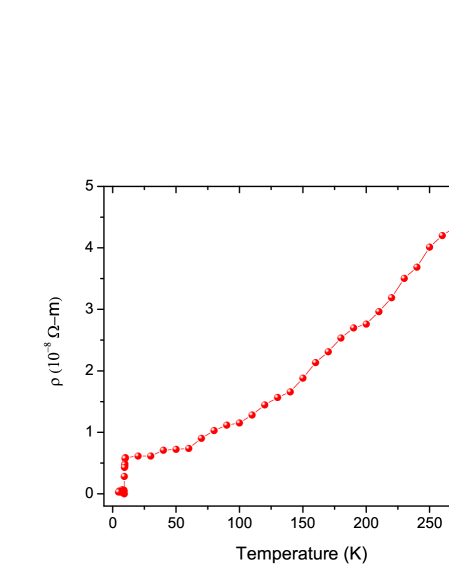
Fig. 3 shows the resistivity as a function of temperature. The characteristic is typical of a metallic compound where the resistivity decreases with temperature. At lower temperature the resistivity shows the transition to the superconducting state with zero resistance at 9.1 K.
II.3 Point Contact Spectroscopy
With PCS junctions we were able to study the superconducting state, the contacts were prepared in two distinct manner: crossing a W(Au) thin wire of 5 m diameter over one edge of the crystal, or on a flat surface of it. The sample was glued to a glass substrate with Oxford varnish in order to have good thermal contact. The normal electrode wire (W(Au)) was stretched over the sample to touch an edge or a flat surface of the crystal.
As mentioned before, several conditions need to be fulfilled when measuring PCS, one is the working regime. Whereas smaller the area of the contact more relevant (the spectroscopic characteristics) will be. The most reliable electronic characteristics will be obtain when heating effects are completely eliminated or are small Blonder ; Daghero ; Duif ; Jansen ; Branislav .
Accordingly, the best working conditions to study spectroscopic characteristics will be when a junction is in the ballistic regime. In it the injected electrons only will be scattered into the studied compound by elementary excitations; phonons, magnons, etc. Jansen ; Escudero ; REscudero ; Sinchenko . We have to note that this regime is quite difficult to achieve, because the size of the contact must be much smaller than the electronic mean free path of the compound under study . This regime in many circumstances may be practically impossible to achieve considering that in superconducting materials frequently the mean free path () may be very small of the order of a few nanometers Daghero ; Duif ; Michael ; Terry ; Jansen ; Blonder ; Strijkers ; Kedves ; Raymond ; Branislav .
Also, we have to mention that at this moment we do not have information about the size of the electronic means free path of this compound. But however, because the values of PCS differential resistances determined at zero bias voltage, which are of the order of 30 - 50 , we may estimated that our experimental determination of the spectroscopic characteristics will be located close to the ballistic regime and in the worst case into the diffuse limit but far away to the Maxwell regime, where heating effect are very important and the spectroscopic features are totally distorted. All this consideration were taking into account according as mentioned by Yanson, et al. yanson . Lastly another important condition to be fulfilled and used to characterize the type of junction is related to the parameter given by the BTK model. It tell us if the spectroscopic characteristic are type tunnel or PCS. The size of this parameter was determined in our studies at 3.
The electronic equipment used to characterize the junctions and to obtain, first the differential resistance, and after the differential conductance as functions of the bias voltage (, and vs , respectively) was the modulation technique with lock-in amplifier and bridge wolf ; Adler and a MPMS Quantum Design system as a cryostat.


The studies of the energy gap in Zr0.97V0.03B2 were performed with PCS. The differential conductance, was obtained by numerical inversion of the differential resistance at different temperatures from 1.7 to 20 K. At low temperature is well known that the differential conductance is directly proportional to the density of electronic states wolf . In Fig. 4 we show results of the measured characteristics associated with the energy gap feature. In this figure close to 6.5 K we see a small hump that rapidly grows as the temperature descends. The hump is dramatically deformed at 3 K emerging two symmetrically identical peaks around zero bias voltage. These peaks give a clear evidence of the regime of behavior of the PCS with this characteristic we calculate the valor of the parameter compared to the shape of the curves with the BTK model. A note of caution must be mentioned; all PCS spectroscopic characteristics reported here were reproducible and with stable characteristics. PCS with values of differential resistance below 20 were discarded, and only PCS with values above 30 were used as spectroscopic material. Values of differential resistance above 50 were not used because presented noisy characteristics. The number of junctions prepared and measured were more than 40 - 47, but the reported data were taken from only the very reproducible junctions. From this we selected the more stables junctions that show reproducible characteristics.
The size of the energy gap at the minimum accessible temperature of our equipment, 1.7 K, was 2 7.2 meV obtained by fitting the experimental data with BTK model. The shape of the normalized differential conductance corresponds to a regime with Strijkers ; Lucas ; Srikanth .
In Fig. 5 we show the normalized differential conductance at two different temperatures, 1.7 and 10 K. Note the dramatic changes when the material is at low temperature in the superconducting state. The feature at 1.7 K is typical of a normal-metal/insulator/superconductor junction in the ballistic regime Sheet ; Gennes ; Lucas ; Strijkers ; Srikanth ; Blonder ; Jansen ; Daghero ; Park .
II.4 Experimental Data and BTK Model
Fig. 6 shows the fitting of experimental data to the BTK model. The fit and the experimental data are quite similar at low temperatures, from 1.7 to 6 K. At temperatures above 6 K the feature associated to the energy gap was not fitted, the feature related to the gap was not seen. The dependence of gap feature with temperature was compared with the BCS model, and the fit was performed in ranges from about 7.5 - 8.5 K, as shown in Fig. 7. It is important to mention that according to our measurements the ratio 2()/KBTC extrapolated to zero temperature is approx 8.95, implying a very strong coupling limit for this superconductor Schmidt .
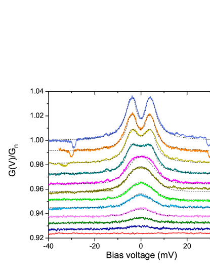

Despite that unknown size of the mean free path of the Zr0.97V0.03B2, we can say that the majority of the point contacts taken into account for this work were operating within the ballistic and diffuse regime. This observation was based in comparison between the experimental spectra and the obtained by the BTK model. In general, the resistance values of the different point contacts used and measured at zero bias voltage varied from 30 - 50 .
In addition to the determination of the energy gap, we also performed measurements at higher bias voltages beyond the feature associated with the superconducting gap, this is shown in Fig 4. to 6. Here is shown features related to the superconducting state ( 33 meV), as possible resonances of the energy gap. Those characteristics can not be simulated with the BTK model and already been observed by other workers in the field Sheet ; Strijkers ; Shan ; DeWilde ; wolf , the given explanations are controversial Shan ; Rourke ; Sheet ; Bashlakov ; Hohn ; Yansonw .
III Conclusions
We have presented experimental results of the behavior of the energy gap in the Zr0.97V0.03B2 superconducting compound. Analysis of the experimental data using the BTK theoretical model give us values of the size of the energy gap which at low temperature was determined to be 2 meV, also we determined the value for the ratio 2(0)/KBTC 8.95 which suggests a superconductor in the strong coupling regime.
Acknowledgements.
This work was partially supported by grants by DGAPA-UNAM project IN106014, CONACyT México. López-Romero thanks to CONACyT-México for a scholarship and DGAPA-UNAM, IN106014. We also thanks Joaquín Morales, Alberto López, R. Reyes, and F. Silvar for technical support and helium provisions.References
- (1) Ivar Giaever, Phys. Rev, 5, 4, 1960.
- (2) Ivar Giaever and Karl Megerle, Phys. Rev. lett. 122, 4, 1961.
- (3) E. L. Wolf, Principles of electron tunneling spectroscopy, Oxford University Press, New York, 1989.
- (4) Yu.V. Sharvin, Sov, Phys. JETP 21, 655, 1965.
- (5) I. K. Yanson, Sov.JETP 39, 1974.
- (6) I. K. Yanson, I. O. Kulik, and A. G. Batrak, Journal of Low Temperature Physics, 42, 5, 1981.
- (7) I. K. Yanson, Y. N. Shalor, JETP, 44, 148, 1976.
- (8) S. K. Upadhyay, A. Palanisami, R. N. Louie, and R. A. Buhrman, Phys. Rev. Lett. 81, 15, 1998.
- (9) C. J. Muller, J. M. van Ruitenbeek, L. J. de Jongh, Physica C, 191, 485, 1992.
- (10) R. Escudero, F. Morales, Phys. Rev. 150, 715-719, 1994.
- (11) D. Daghero and R. S. Gonnelli, arXiv:0912.4858v1, 2009.
- (12) A. M. Duif, A. G. M. Jansen, and P. Wilder, J. Phys.: Condens. Matter. 1, 3157-3189, 1989.
- (13) A. G. M. Jansen, A. P. van Gelder and P. Wyder, J. Phys. C: Solid St. Phys. 13, 6073-118, 1980.
- (14) G. Wexler, Proc. Phys. Soc. London 89, 927-941, 1966.
- (15) G. E. Blonder, M. Tinkham, T. M. Klapwijk, Phys. Rev. B, 25, 7, 1982.
- (16) G. J. Strijkers, Y. Ji, F. Y. Yang, and C. L. Chien, Phys. Rev, B, 63, 104510, 2001.
- (17) Michael Tinkham, Introduction to superconductivity, second edition, McGraw Hill, Inc. 1996.
- (18) Terry. P. Orlando and Kevin A. Delin, Foundations of applied superconductivity, Addison- Wesley Publishing Company, 1990.
- (19) F. J. Kedves, S. Meszaros, K. Vad, G. Halasz, B. Keszei, and L. Mihaly, Solid State Commun, 63, 991-992, 1987.
- (20) Raymond A. Serway and Robert J. Beichner, Physics for scientists and engineers with modern physics, 9th edition, Thomson, 2013.
- (21) I. K. Yanson, YU. G. Naidyuk, O. E. Kvitnitskaya, V. V. Fisun, N. L. Bobrov, P. N. Chubov, V. V. Ryabovol, G. Behr, W. N. Kang, E.-M. Choi, H.-J. Kim, S.-I. Lee, T. Aizawa, S. Otani, and S.-L. Drechsler Modern Physics Letters B, 17, 10, 2003.
- (22) V. A. Gasparov, N. S. Sidorov, I. I. Zver’kova, and M. P. Kulakov, Jetp Letters, 73, 10, 2001.
- (23) V. A. Gasparov, Jept Letters, 80, 5, 2004.
- (24) Soon-Gil Jung, Journal of applied physics 114, 133905, 2013.
- (25) S. T. Renosto, Phys. Rev. B 87, 174502, 2013.
- (26) J. Wang, Z.X. Shi, H. Lv, T. Tamegai, Physica C, 445-448, 462-465, 2006.
- (27) Branislav Nikolić and Philip B. Allen, arXiv:cond-mat/9811296v1 Nov 1998.
- (28) R. Escudero and F. Morales, Phys. Rev. B, 49, 21, 1994.
- (29) A. A. Sinchenko, Phys. Rev. B, 70, 7, 1999.
- (30) I.K.Yanson, et al., Modern Physics Lett. B, Vol. 17, No. 10, 11, 12 (2003).
- (31) J. G. Adler and J. E. Jackson, Rev. Sci. Instrum. 37, 1049, 1966.
- (32) Lucas Janson, et al.,ArXiv:1110.6254v1 [physics.ed-ph], 2011.
- (33) H. Srikanth and A. K. Raychaudhuri, Physica C: Superconductivity, 190, 229-233, 1992.
- (34) W.K Park and L H Greene, J. Phys. Condens. Matter 21, 10, 2009.
- (35) Goutam Sheet, S. Mukhopadhyay, and P. Raychaudhuri, Phys. Rev. B, 69, 134507, 2004.
- (36) P. G. de Gennes, Boundary Effects in Superconductors, Review of modern physics, 36, 1, 1964.
- (37) P. Múller, A. V. Ustinov and V. V. Schmidt, The Physics of superconductors: Introduction to Fundamentals and Applications, Springer, Berlin, 1997.
- (38) L. Shan, et al., Phys. Rev. B, 68, 144510, 2003.
- (39) Y. DeWilde, et al., Phys. Rev. lett. 80, 1, 1998.
- (40) P. M. C. Rourke, et al.,Phys. Rev. Lett. PRL 94, 107005, 2005.
- (41) D. L. Bashlakov, et al., Supercond. Sci. Technol. 18, 1094–1099, 2005.
- (42) N. Hohn, et al.,Z. Phys. B Condensed Matter 69, 173-178, 1987.
- (43) I.K. Yanson, N.L. Bobrov, C.V. Tomy, D.McK. Paul, Physica C, 334, 33–43, 2000.