Observation of pure inverse spin Hall effect in ferromagnetic metals by FM/AFM exchange bias structures
Abstract
We report that the spin current generated by spin Seebeck effect (SSE) in yttrium iron garnet (YIG) can be detected by a ferromagnetic metal (NiFe). By using the FM/AFM exchange bias structure (NiFe/IrMn), inverse spin Hall effect (ISHE) and planar Nernst effect (PNE) of NiFe can be unambiguously separated, allowing us to observe a pure ISHE signal. After eliminating the in plane temperature gradient in NiFe, we can even observe a pure ISHE signal without PNE from NiFe itself. It is worth noting that a large spin Hall angle (0.098) of NiFe is obtained, which is comparable with Pt. This work provides a kind of FM/AFM exchange bias structures to detect the spin current by charge signals, and highlights ISHE in ferromagnetic metals can be used in spintronic research and applications.
How to generate, manipulate, and detect spin currents () is a fundamental issue in spintronic research Wolf et al. (2001); Žutić et al. (2004). Spin injection from a ferromagnetic metal Johnson and Silsbee (1985); Jedema et al. (2001), spin pumping Saitoh et al. (2006); Mosendz et al. (2010), spin Hall effect (SHE) Kato et al. (2004); Valenzuela and Tinkham (2006), and spin Seebeck effect (SSE) Uchida et al. (2008); Bauer et al. (2012); Uchida et al. (2010a, b, c); Li et al. (2014); Adachi et al. (2013) provide several ways to generate a spin current. Especially SSE in ferromagnetic insulators (FI) Uchida et al. (2010a, b, c); Li et al. (2014) has attracted much attention for a pure spin current can be generated without any charge flow. Inverse spin Hall effect (ISHE) Saitoh et al. (2006); Kimura et al. (2007) in heavy metals with strong spin-orbit coupling (SOC) such as Pt is often used to detect the spin current by charge signals: , where is the ISHE electric field, is the spin Hall angle, is the resistivity and is the unit vector of spin.
As the inverse effect of anomalous Hall effect (AHE), ISHE in ferromagnetic metals provides a possibility to detect the spin current as well. Recently, several works focus on using ferromagnetic metals instead of metals with strong SOC to detect the spin current generated by SSE in FI Miao et al. (2013); Tian et al. (2015); Wu et al. (2014). However, additional anomalous Nernst effect (ANE) and planar Nernst effect (PNE) in the ferromagnetic metal itself is often mixed with the ISHE signal in longitudinal and transversal spin Seebeck measurement respectively. Therefore, in transversal spin Seebeck measurement, unambiguous separation of PNE and ISHE signals will be an important progress, not only for exploring the physical mechanism of ISHE in ferromagnetic metals, but also for future applications in detecting spin currents.
Exchange bias phenomenon in the ferromagnetic (FM)/antiferromagnetic (AFM) interface Koon (1997); Berkowitz and Takano (1999) can provide a shift field () of the magnetization hysteresis loop, when cooling down to Neel temperature () with a static magnetic field, which has been used in spin valve structures for several years. This phenomenon is associated with the interfacial exchange anisotropy between FM and AFM, and FM tends to align parallel with uncompensated spins of AFM at the interface. Therefore, FM has a unidirectional anisotropy.
In this work, NiFe/IrMn exchange bias structure has been employed to detect the spin current in NiFe originating from SSE in YIG, Cu was inserted between NiFe and YIG to decrease the exchange coupling and to eliminate the possible magnetic proximity effect Huang et al. (2012); Lu et al. (2013). The temperature gradient is mainly in plane and along the exchange bias field axis. However, PNE from NiFe itself will be involved in ISHE voltages Pu et al. (2006); Avery et al. (2012). This structure can separate the magnetization reversal process of YIG and NiFe. As a result, ISHE and PNE which related to the magnetization state of YIG and NiFe respectively could be separated as well.
The detail multilayer film structure is GGG/YIG/Cu(t nm)/NiFe(5 nm)/IrMn(12 nm)/Ta(5 nm). Firstly, a 3.5 m YIG film was grown on a 300 m GGG(111) substrate using liquid phase epitaxial method. Then upper films were deposited using an ultrahigh vacuum magnetron sputtering system (ULVAC) at a pressure of 0.16 Pa and a power of 120 W. In order to provide a clear interface between YIG and Cu, the YIG surface was cleaned for 60 s by Ar plasma in the vacuum chamber before deposition. A 100 Oe magnetic field was applied during deposition, which could induce an easy magnetization axis and an exchange bias of NiFe. Films were patterned by photolithography combined with Ar ion etching. Both of the electrodes A and C are of 10 m 100 m in size, and the size of electrode B is 50 m 100 m (m). The spacing between A (B) and B (C) is 10 m.
Fig. 1(a) shows the schematic illustration of the measurement method. Electrode A and C were used to heat the YIG film by electric currents (Keithley 2440), which induced a transverse temperature gradient mainly along y axis, and the heating power . Because of SSE in YIG, produces a spin accumulation at the interface between YIG and electrode B, and then the spin current is injected to electrode B. By measuring the voltage along x axis in electrode B (Keithley 2182A), the spin current can be detected by means of ISHE, as shown in Fig. 1(b). The physical property measurement system (Quantum Design PPMS) was used to apply the magnetic field and control the temperature. All measurements were performed at room temperature.
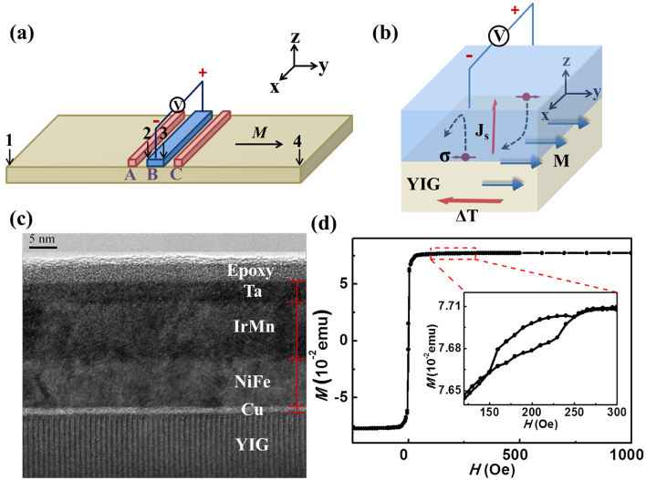
The cross-section high resolution transmission electron microscopy (HRTEM) of GGG/YIG/Cu(3 nm)/NiFe(5 nm)/IrMn(12 nm)/Ta(5 nm) sample was observed by Tecnai G2 F20 S-TWIN (200 kV). HRTEM results are shown in Fig. 1(c). The high quality YIG single crystal structure is formed on the GGG(111) substrate, and the epitaxial direction of YIG film is also along (111) direction. Four metal layers deposited by magnetron sputtering are continuous and flat, and each interface especially the interface between YIG and Cu is very clear and sharp. The spin current is injected from YIG to above films, so the clear YIG/Cu interface is very important.
The magnetic hysteresis loop of GGG/YIG/Cu(5 nm)/NiFe(5 nm)/IrMn(12 nm)/Ta(5 nm) sample was measured by a vibrating sample magnetometer (VSM, MicroSense EZ-9) with magnetic field applied along y axis (also the axis of the exchange bias field), as shown in Fig. 1(d). YIG is a very soft magnetic material and the saturation field () of YIG is less than 10 Oe. The inserted figure shows the minor M-H loop from NiFe, and (200 Oe) is enough to distinguish the magnetization reversals of NiFe and YIG. Besides, the magnetic moment from YIG is very large due to its larger thickness.
As reported in previous works Uchida et al. (2008); Bauer et al. (2012); Uchida et al. (2010a, b, c); Li et al. (2014), firstly we used a 10 nm thick () Pt film to detect induced by SSE in YIG. A 300 nV ISHE voltage is observed as mA in electrode C is applied with field along y axis [Fig. 2(a)]. ISHE voltages were not observed when field was applied along x and z axis respectively, which confirms the SSE scenario. When a 3 nm metal Cu layer is inserted between Pt and YIG to eliminate the magnetic proximity effect between YIG and Pt, still a spin current can pass without remarkable dissipation, as proven by the ISHE voltage observed in this case. However, once a 3 nm insulator MgO layer is inserted to block from YIG, the ISHE voltage completely disappears. These results confirm that the voltage is induced by injected from YIG. This voltage does not come from Pt or YIG alone, which could be proven by the absence of the voltage in YIG/Cu and Si-SiO2/Pt reference samples.
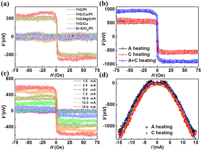
When we changed the heating electrode from C to A: , , and , , represent the temperature of point B, 1, 4 when heating A and C respectively; , and represent the temperature of point B, 1 and 4 when heating A and C simultaneously. , , due to the geometrical symmetry. So the ISHE voltage: , where , is the spin Hall angle of Pt, is the spin injection efficiency, is the aspect ratio and is the spin Seebeck coefficient Uchida et al. (2008). The ISHE voltage is almost the same when changing the heating electrode from C to A, as shown in Fig. 2(b). When heating A and C at the same time, the ISHE voltage is enhanced due to higher temperature gradient: [Fig. 2(b)].
We also measured the curves with fields along y axis larger than of YIG ( 20 Oe) and then obtained the difference between them, namely spin dependent ISHE voltages: . Fig. 2(c) and Fig. 2(d) show the relationship between ISHE voltages and heating currents: , which confirms that the ISHE signal is thermal related. And the curves nearly coincide after changing the heating electrode from C to A.
Furthermore, we changed the spin current detector Pt with the exchange bias structure: Cu(5 nm)/NiFe(5 nm)/IrMn(12 nm)/Ta(5 nm), and heated the electrode C with 15 mA . The heating current generates not only in YIG, but also in electrode B, which induces a PNE voltage in NiFe. By using the exchange bias structure, magnetization reversals of NiFe and YIG are separated, as can be seen in Fig. 1(d). As a result, ISHE (related to magnetization of YIG) and PNE (related to magnetization of NiFe) are separated as well. As shown in Fig. 3(a), a 500 nV PNE voltage is observed and the center field of the PNE curve locates at 120 Oe. This shift field is smaller than the from M-H curves for two reasons: one is that the film is patterned, and another is that the temperature of the electrode B increases when heating C.
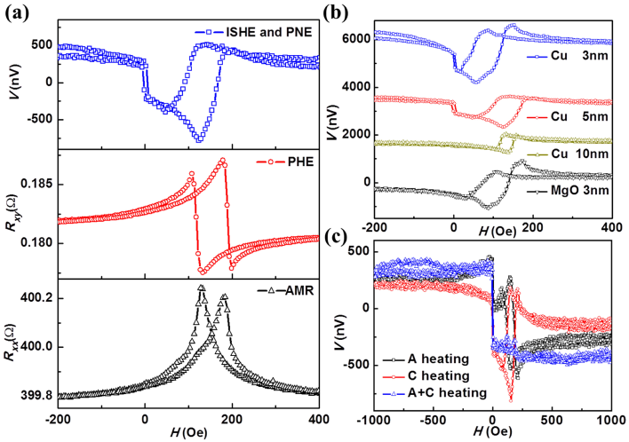
It is especially attractive that a 250 nV is observed near zero magnetic field and the voltage saturates at a field less than 10 Oe, which is similar to the signal in YIG/Pt sample. And the sign of the ISHE voltage in NiFe is the same with that in Pt. Transport properties only depend on the magnetization of NiFe, because YIG is an insulator. Anisotropic magnetoresistance (AMR) and planar Hall effect (PHE) reflect the magnetization state of NiFe and share the similar origin with PNE, which only have a signal near 150 Oe, and do not have an obvious signal near 0 Oe. Especially PHE almost have the same curve with PNE, the only difference is that one is from the electric current, and the other is from the thermal current. These prove that the signal near 0 Oe is not from PNE in NiFe, but from ISHE in NiFe induced by SSE in YIG, which can also be confirmed by M-H curves in Fig. 1(d).
When the thickness of inserted Cu varies from 3 nm to 10 nm, three changes emerge as follows: (1) decreases gradually and even disappears due to increased spin relaxation in Cu Kimura et al. (2005) and decreased resistance of electrode B; (2) decreases because temperature gradient in NiFe also decreases; (3) of NiFe increases with thicker Cu because the exchange coupling between NiFe and YIG weakens. On the other hand, once a 3 nm insulator MgO layer is inserted, disappears while still exists under the same precision, as shown in Fig. 3(b), because thermal currents can still conduct even in insulators, but spin currents cannot. These results also confirm that the signal near 0 Oe is not from NiFe itself, such as ANE or PNE.
, and , represent the temperature of boundary 2, 3 of electrode B when heating electrode A and C respectively; , represent the temperature of boundary 2, 3 of electrode B when heating A and C simultaneously. Due to the geometrical symmetry, , , and voltages satisfy the following equations: , where ; , where is the simplified coefficient. When changing the heating electrode from C to A, is opposite in sign, while is the same, as shown in Fig. 3(c). When heating A and C at the same time: , . By eliminating along y axis in NiFe, in NiFe could nearly be cancelled, while is enhanced because of the enhanced in YIG. In this way, we succeed in directly detecting the pure in NiFe without the influence of from itself [Fig. 3(c)]. Besides, along z axis in NiFe will be also enhanced when simultaneously heating A and C. Even in this case, ANE voltages in NiFe are not observed, indicating that along z axis in NiFe is negligibly small.
To further illustrate the ISHE in NiFe, we measured the dependence of and , as shown in Fig. 4. The center field of the PNE curve corresponds to of NiFe, and it decreases with increasing , as shown in Fig. 4(a), because in FM/AFM usually decreases with the increasing temperature, even drops to zero at blocking temperature.
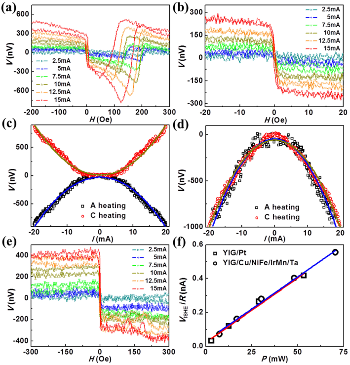
Fig. 4(c) and Fig. 4(d) show the dependence of [V(+250 Oe)-V(+20 Oe)] and [V(+10 Oe)-V(-10 Oe)] respectively, they are both proportional to , confirming their thermal dependence. is opposite in sign when we changed the heating electrode from C to A, while remains unchanged. This difference also confirms that these two signals should come from different origins: one from PNE in NiFe, and another from ISHE in NiFe induced by SSE in YIG. By simultaneously heating A and C, as shown in Fig. 4(e), enhanced pure is observed, while from NiFe itself is totally eliminated.
To quantitatively analyze the spin Hall angle of NiFe, we measured the dependence of in YIG/Pt(10 nm) and YIG/Cu(5 nm)/NiFe(5 nm)/IrMn(12 nm)/Ta(5 nm) samples, as shown in Fig. 4(f). ISHE induced charge currents: , where is the resistance of electrode B. We suppose the coefficient that expresses the efficiency from thermal currents to spin currents in electrode B is the same in these two samples. By linear fitting curves, relative spin Hall angle (NiFe)/(Pt) . By using (Pt) Wang et al. (2014a), we obtain (NiFe) , which is at the same order with (NiFe) measured by spin pumping Wang et al. (2014b). These results show that NiFe almost has a comparable spin Hall angle with Pt. In fact, previous works have suggested strong SOC in 3d transition metals Du et al. (2014); Morota et al. (2011)and connected ISHE with AHE in the ferromagnetic metal (CoFeB) through Mott relation Wu et al. (2014). Strong SOC and ferromagnetic order in NiFe should contribute to the large . By using the exchange bias structure, investigating SHE and ISHE in ferromagnetic metals will become more feasible. As heavy metals with strong SOC, ferromagnetic metals become another promising candidate for detecting spin currents.
In conclusion, firstly a spin current in NiFe is generated by SSE in YIG, and then is detected by charge signals due to ISHE. The NiFe/IrMn exchange bias structure was used to separate ISHE and PNE in NiFe, and inserted Cu can decouple the exchange coupling and rule out the possible magnetic proximity effect between NiFe and YIG, allowing us to observe a pure ISHE signal. By simultaneously heating electrodes in both sides of electrode B, which can eliminate the in plane temperature gradient in NiFe, PNE from NiFe itself is eliminated, while only ISHE is remained. By fitting the curves, we obtain a large spin Hall angle (0.098) in NiFe. This work is crucial to unambiguous confirmation of existence of ISHE in ferromagnetic metals and also to the applications of FM-based ISHE.
Acknowledgements.
This work was supported by the State Key Project of Fundamental Research of Ministry of Science and Technology (MOST) [No. 2010CB934401], the MOST National Key Scientific Instrument and Equipment Development Projects [No. 2011YQ120053] and the National Natural Science Foundation [NSFC, Grant No. 11434014].References
- Wolf et al. (2001) S. A. Wolf, D. D. Awschalom, R. A. Buhrman, J. M. Daughton, S. V. Molnar, M. L. Roukes, A. Y. Chtchelkanova, and D. M. Treger, Science 294, 1488 (2001).
- Žutić et al. (2004) I. Žutić, J. Fabian, and S. D. Sarma, Rev. Mod. Phys. 76, 323 (2004).
- Johnson and Silsbee (1985) M. Johnson and R. H. Silsbee, Phys. Rev. Lett. 55, 1790 (1985).
- Jedema et al. (2001) F. J. Jedema, A. T. Filip, and B. J. van Wees, Nature 410, 345 (2001).
- Saitoh et al. (2006) E. Saitoh, M. Ueda, H. Miyajima, and G. Tatara, Appl. Phys. Lett. 88, 182509 (2006).
- Mosendz et al. (2010) O. Mosendz, J. E. Pearson, F. Y. Fradin, G. E. W. Bauer, S. D. Bader, and A. Hoffmann, Phys. Rev. Lett. 104, 046601 (2010).
- Kato et al. (2004) Y. K. Kato, R. C. Myers, A. C. Gossard, and D. D. Awschalom, Science 306, 1910 (2004).
- Valenzuela and Tinkham (2006) S. O. Valenzuela and M. Tinkham, Nature 442, 176 (2006).
- Uchida et al. (2008) K. Uchida, S. Takahashi, K. Harii, J. Ieda, W. Koshibae, K. Ando, S. Maekawa, and E. Saitoh, Nature 455, 778 (2008).
- Bauer et al. (2012) G. E. W. Bauer, E. Saitoh, and B. J. van Wees, Nature Mater. 11, 391 (2012).
- Uchida et al. (2010a) K. Uchida, J. Xiao, H. Adachi, J. Ohe, S. Takahashi, J. Ieda, T. Ota, Y. Kajiwara, H. Umezawa, Kawai, G. E. W. Bauer, S. Maekawa, and E. Saitoh, Nature Mater. 9, 894 (2010a).
- Uchida et al. (2010b) K. Uchida, H. Adachi, T. Ota, H. Nakayama, S. Maekawa, and E. Saitoh, Appl. Phys. Lett. 97, 172505 (2010b).
- Uchida et al. (2010c) K. Uchida, T. Nonaka, T. Ota, and E. Saitoh, Appl. Phys. Lett. 97, 262504 (2010c).
- Li et al. (2014) P. Li, D. Ellsworth, H. Chang, P. Janantha, D. Richardson, F. Shah, P. Phillips, T. Vijayasarathy, and M. Wu, Appl. Phys. Lett. 105, 242412 (2014).
- Adachi et al. (2013) H. Adachi, K. Uchida, E. Saitoh, and S. Maekawa, Rep. Prog. Phys. 76, 036501 (2013).
- Kimura et al. (2007) T. Kimura, Y. Otani, T. Sato, S. Takahashi, and S. Maekawa, Phys. Rev. Lett. 98, 156601 (2007).
- Miao et al. (2013) B. F. Miao, S. Y. Huang, D. Qu, and C. L. Chien, Phys. Rev. Lett. 111, 066602 (2013).
- Tian et al. (2015) D. Tian, Y. F. Li, D. Qu, X. F. Jin, and C. L. Chien, Applied Physics Letters 106, 212407 (2015).
- Wu et al. (2014) S. M. Wu, J. Hoffman, J. E. Pearson, and A. Bhattacharya, Appl. Phys. Lett. 105, 092409 (2014).
- Koon (1997) N. Koon, Phys. Rev. Lett. 78, 4865 (1997).
- Berkowitz and Takano (1999) A. E. Berkowitz and K. Takano, J. Magn. Magn. Mater. 200, 552 (1999).
- Huang et al. (2012) S. Y. Huang, X. Fan, D. Qu, Y. P. Chen, W. G. Wang, J. Wu, T. Y. Chen, J. Q. Xiao, and C. L. Chien, Phys. Rev. Lett. 109, 107204 (2012).
- Lu et al. (2013) Y. M. Lu, Y. Choi, C. M. Ortega, X. M. Cheng, J. W. Cai, S. Y. Huang, L. Sun, and C. L. Chien, Phys. Rev. Lett. 110, 147207 (2013).
- Pu et al. (2006) Y. Pu, E. Johnston-Halperin, D. D. Awschalom, and J. Shi, Phys. Rev. Lett. 97, 036601 (2006).
- Avery et al. (2012) A. D. Avery, M. R. Pufall, and B. L. Zink, Phys. Rev. Lett. 109, 196602 (2012).
- Kimura et al. (2005) T. Kimura, J. Hamrle, and Y. Otani, Phys. Rev. B 72, 014461 (2005).
- Wang et al. (2014a) H. L. Wang, C. H. Du, Y. Pu, R. Adur, P. C. Hammel, and F. Y. Yang, Phys. Rev. Lett. 112, 197201 (2014a).
- Wang et al. (2014b) H. L. Wang, C. H. Du, P. C. Hammel, and F. Y. Yang, Appl. Phys. Lett. 104, 202405 (2014b).
- Du et al. (2014) C. Du, H. Wang, F. Yang, and P. C. Hammel, Phys. Rev. B 90, 140407(R) (2014).
- Morota et al. (2011) M. Morota, Y. Niimi, K. Ohnishi, D. H. Wei, T. Tanaka, H. Kontani, T. Kimura, and Y. Otani, Phys. Rev. B 83, 174405 (2011).