Identification of Topological Surface State in PdTe2 Superconductor by Angle-Resolved Photoemission Spectroscopy
Abstract
High resolution angle-resolved photoemission measurements have been carried out on transition metal dichalcogenide PdTe2 that is a superconductor with a Tc at 1.7 K. Combined with theoretical calculations, we have discovered for the first time the existence of topologically nontrivial surface state with Dirac cone in PbTe2 superconductor. It is located at the Brillouin zone center and possesses helical spin texture. Distinct from the usual three-dimensional topological insulators where the Dirac cone of the surface state lies at the Fermi level, the Dirac point of the surface state in PdTe2 lies deep below the Fermi level at 1.75 eV binding energy and is well separated from the bulk states. The identification of topological surface state in PdTe2 superconductor deep below the Fermi level provides a unique system to explore for new phenomena and properties and opens a door for finding new topological materials in transition metal chalcogenides.
PACS: 73.20.At, 74.70.-b, 79.60.-i, 74.25.Jb
Topological insulators are a new quantum state of matter with insulating bulk state and protected conducting edge or surface states that originate from its unique bulk band topology.RevHasan ; RevZhang The concept of topological insulators has been extended to topological superconductors that have attracted particular attention because they have a full pairing gap in the bulk and gapless surface states consisting of Majorana fermions.RevHasan ; RevZhang ; ZhangTSC The topological surface state exhibits unique electronic structure and spin texture which not only have potential applications in spintronics and quantum computing,RevQXL ; RevMoore2 but also provide a promising platform for realizing exotic quantum phenomena,QiXL2008 ; RLi2010 ; QiXL2009 ; FuLPRL ; YuR including the revelation of Majorana fermions.MajoranaMajorana ; WilczekMajorana The topological surface state has been observed mainly in the three-dimensional topological insulators Bi2(Se,Te)3 and related compounds, with a single Dirac cone observed near the Fermi level.YXia ; HJZhang ; YLChen The discovery of topological surface state in new class of materials, particularly in superconducting materials,CavaCuBiSe ; HasanCuBiSe is of critical importance in realizing new quantum phenomena and potential applications.
The transition metal chalcogenides have been a rich playground to discover new materials with diverse physical phenomena and properties, such as the charge density wave,Moncton ; Wilson1975 superconductivity,Smaalen ; Wilson1969 ; Finlayson ; Roberts ; Sipos ; Pyon ; JJYang extremely large magneto-resistance,Mazhar ; PLCai structural phase transition and strong spin-orbit interaction,Ootsuki2013 ; Ootsuki2014JPSJ ; Ootsuki2014PRB and materials like MoS2 with application potentials.Novoselov ; KFMak ; Splendiani ; Radisavljevic ; Yoon ; Duerloo ; YiZhang However, there have been few reports related to the discovery of topological materials in the transition metal chalcogenides. In this Letter, we report the first time revelation of topological surface state in a transition metal dichalcogenide PdTe2 that is also a superconductor with Tc1.7 K. By carrying out high resolution angle-resolved photoemission (ARPES) measurements on PdTe2, combined with the theoretical calculations and topological invariant analysis, we have identified a topologically nontrivial surface state in PdTe2 with a Dirac point deep below the Fermi level at a binding energy of 1.75 eV. The calculated spin texture of the surface state shows right-handed spin chirality for the upper Dirac branch and the left-handed for the lower one as in usual topological insulators. The discovery of topological surface state in PdTe2 superconductor deep below the Fermi level provides a new platform to explore for new phenomena and properties related to topological materials.
High quality single crystals of PdTe2 were obtained by the self-flux method. The ARPES measurements were performed on our lab photoemission system equipped with the Scienta R4000 electron energy analyzer.GDLiu ; YLiu We used the Helium discharge lamp with three kinds of photon energies: He I ( eV), He I ( eV) and He II( eV), as the photon source for the ARPES measurements. The overall energy resolution used is 10 meV and the angular resolution is 0.3∘. The Fermi level (EF) was referenced by measuring the Fermi edge of a clean polycrystalline gold electrically connected to the sample. The crystals were cleaved in situ and measured at a temperature of K in vacuum with a base pressure better than 510-11 Torr.
The electronic structure of PdTe2 was calculated by performing the first-principle calculation by WIEN2K package, which is based on the full potential linearized augmented plane wave (LAPW) method.Blaha The lattice constants we used here are Å and Å for PdTe2, taking a space group of .McCarron ; Finlayson ; SJobic ; WSKim The Brillouin zone integration was performed on a regular mesh of points. The muffin-tin radii () of Pd and Te atoms are both 2.50 bohr. The largest plane-wave vector was given by . The spin-orbit coupling (SOC) was included self-consistently in all calculations. To see the topological surface states, we construct a tight-binding model using the projected Wannier functions, which can reproduce the GGA band structure precisely.
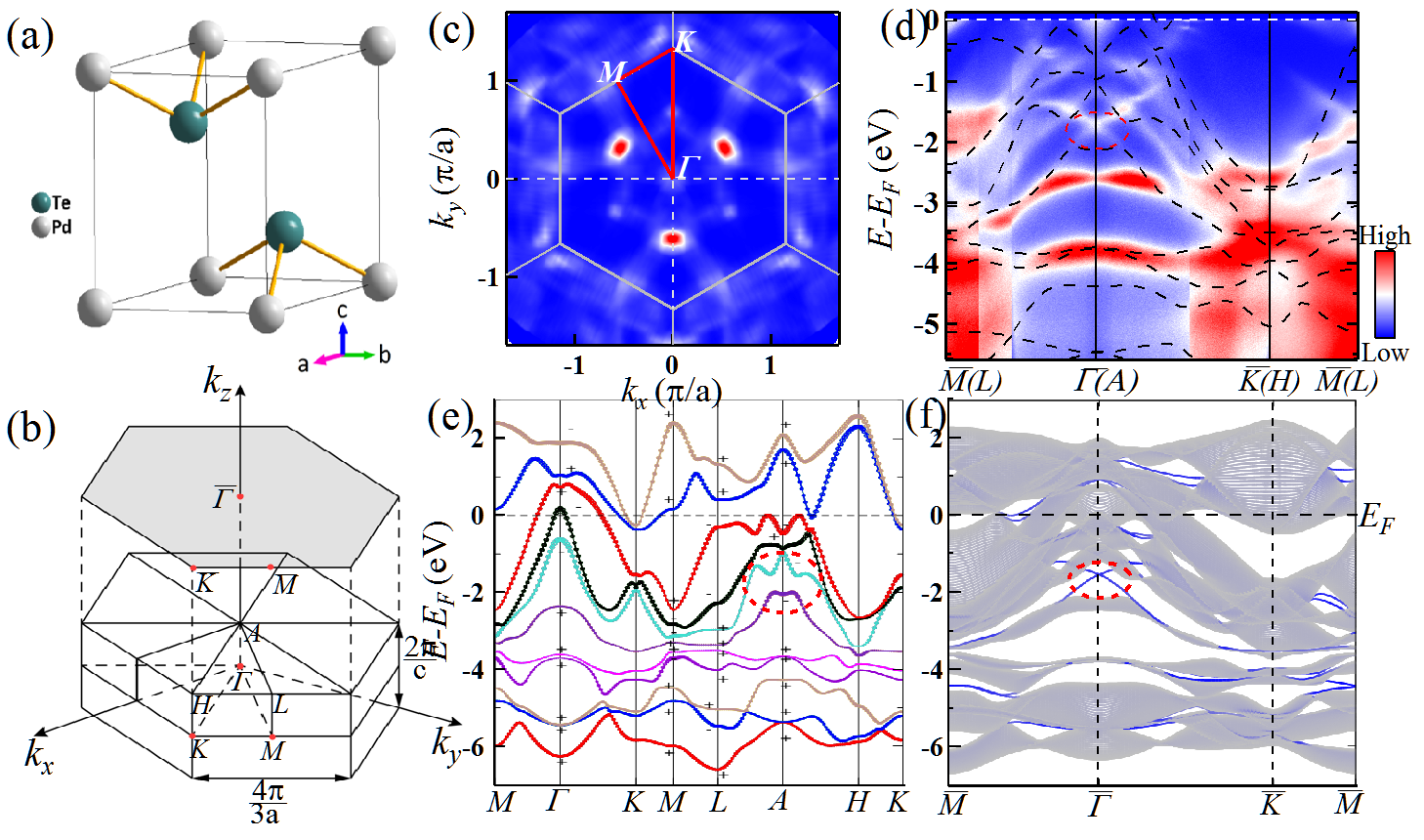
Figure 1 shows the crystal structure, the corresponding bulk and surface Brillouin zones, and the calculated and measured electronic structures of PdTe2. The crystal structure of PdTe2 (Fig. 1(a)) is polymeric CdI2-type with the (No. 164) space group.McCarron ; Soulard ; SJobic ; WSKim ; JPJan The corresponding bulk Brillouin zone is a hexagonal prism, as shown in Fig. 1b together with the projected (001) surface Brillouin zone. The measured Fermi surface of PdTe2 (Fig. 1(c)) exhibits a complex topology with a three-fold symmetryYLiu . The overall band structure of PdTe2 (Fig. 1(d)), measured along high symmetry directions and over a large energy range (06 eV), display multiple densely-arranged bandsYLiu . In order to understand the band structures we measured, we have performed the first-principle calculations with spin-orbit coupling by GGA methodPerdew . Because of the strong three dimensionality of the electronic structures of PdTe2,JPJan ; GYGuo ; Orders the calculated band structure is presented in two different planes and (Fig. 1(e)). By comparing the measured band structure (Fig. 1(d)) with the calculations (Fig. 1e), we noticed the band structures seem more like that calculated in the plane, but still with a prominent discrepancy, as we have shown by overlying the theoretical calculated bands along direction(black dashed lines in Fig. 1(d)) with the experiment data. The large discrepancy prompted us to check for possible reason on the inconsistency between the experiment and the calculations. Interestingly, we notice there is an obvious X-shaped band structure popping out at the Brillouin zone center(Fig. 1(d)) which is absent in the calculation in Fig. 1(e). We suspect whether there is a Dirac cone-like surface state here.
In the calculated band structure of PdTe2 (Fig. 1(e)), there are eleven bands in the covered energy range -7 eV3 eV that are all from strongly hybridized bands between Pd 4- and Te 5-orbitalsJPJan ; GYGuo ; YLiu . To study the topological nature of these bands, we use ”+” and ”-” to describe the parity for each band. There is a band inversion at point at 2 eV below the Fermi level EF. We cut a curved Fermi level at 2 eV below , and calculate the time-reversal invariant parameter as shown in Table 1. The results point to a possible existence of topological nontrivial surface state in PdTe2. We then calculate the semi-infinite (001) surface state of a 40 layer slab based on the TB hamiltonian from Projected Wannier functions and presented in Fig. 1(f). It exhibits a prominent surface state between the binding energy of 1.5 eV and 2.5 eV at . We notice that in the calculated energy window (3-7 eV), all the surface states are merged together with the bulk states, except for this outstanding topological surface state near at the binding energy of 1.75 eV, and some surface states across the Fermi level along the direction. Our measured ARPES data in Fig. 1(d) shows a remarkable agreement with the Dirac cone-like surface state at 2 eV binding energy from the surface state calculations (Fig. 1(f)). The identification of surface states in PdTe2 solves the discrepancy found previously between the ARPES measurements and theoretical calculations.YLiu
| TRIM point | (3) | () | ||
|---|---|---|---|---|
| Parity |
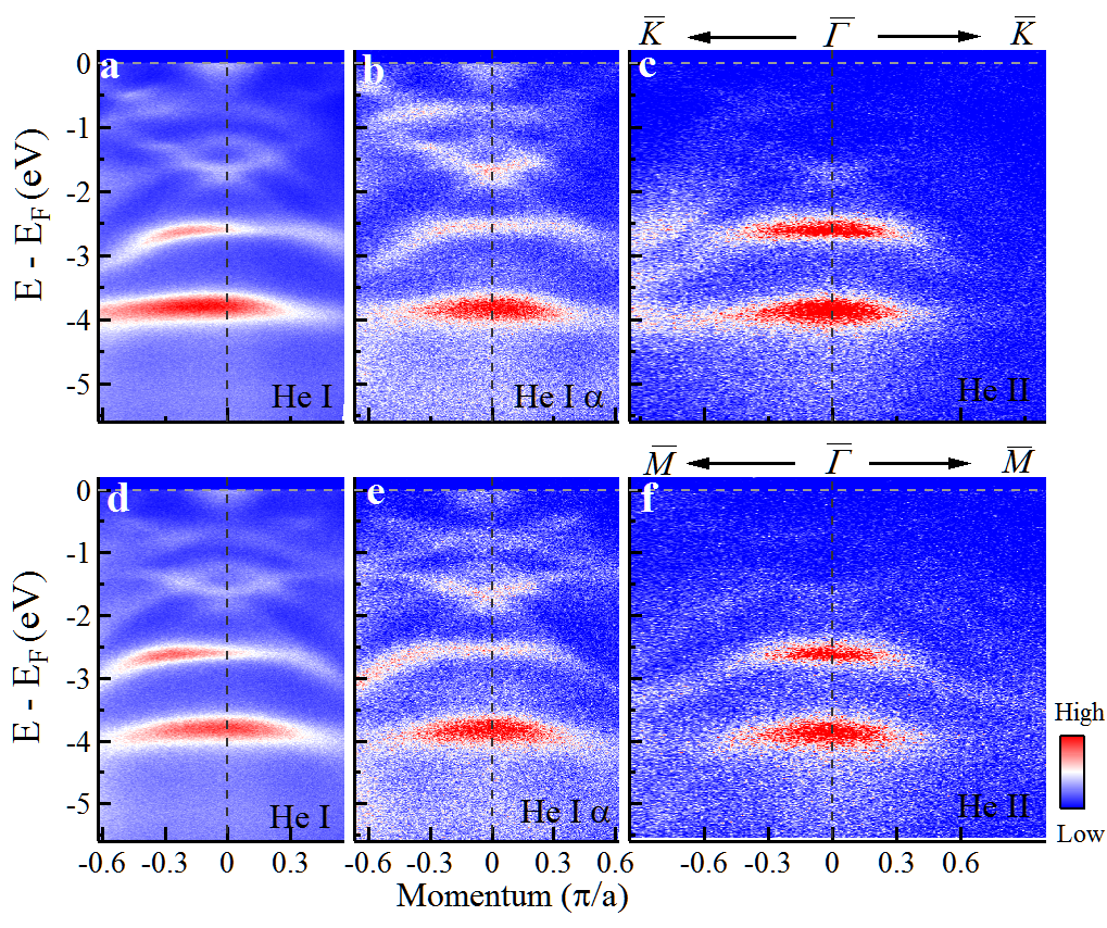
To verify the surface state nature of the measured bands, we performed photon-energy dependent measurements to seek for its two-dimensional character: the surface state will not change with kz. We used three different photon energies to measure the same PdTe2 sample: =21.218 eV, 23.087 eV and 40.8 eV. The measurements were carried out along two high-symmetry directions: (upper panel in Fig. 2) and (lower panel in Fig. 2). Based on our previous work on the inner potential =18.8 eV for PdTe2,YLiu the corresponding kz is estimated to be 5/c for =21.218 eV, 5.13/c for =23.087 eV and 6.22/c for =40.8 eV. This indicates that, for the He I (21.218 eV) and He I (23.087 eV) lines, the ARPES detected planes are close to the plane, while for the He II (40.8 eV) line, it is close to the plane. It is known that the bulk electronic structure of PdTe2 exhibits strong three-dimensionality,JPJan ; GYGuo ; Orders ; YLiu and small variation of kz can generate obvious change of the band structureYLiu . It is clear from Fig. 2 that the low energy features (01.5 eV binding energy) and spectral intensity show strong variation with the photon energy change, reflecting their dominant bulk character. But the Dirac-cone-like bands near 1.75 eV in the Brillouin zone center appear to be quite robust against the change of the photon energy in terms of its energy position and intensity. This is consistent with its nature of being from the surface state. We also notice that the two high energy bands near 2.5 eV and 4.0 eV also do not show strong variation with photon energy change. As seen in Fig. 1(f), this can be understood because they have a large contribution from the surface states, especial for the band at 4 eV binding energy.
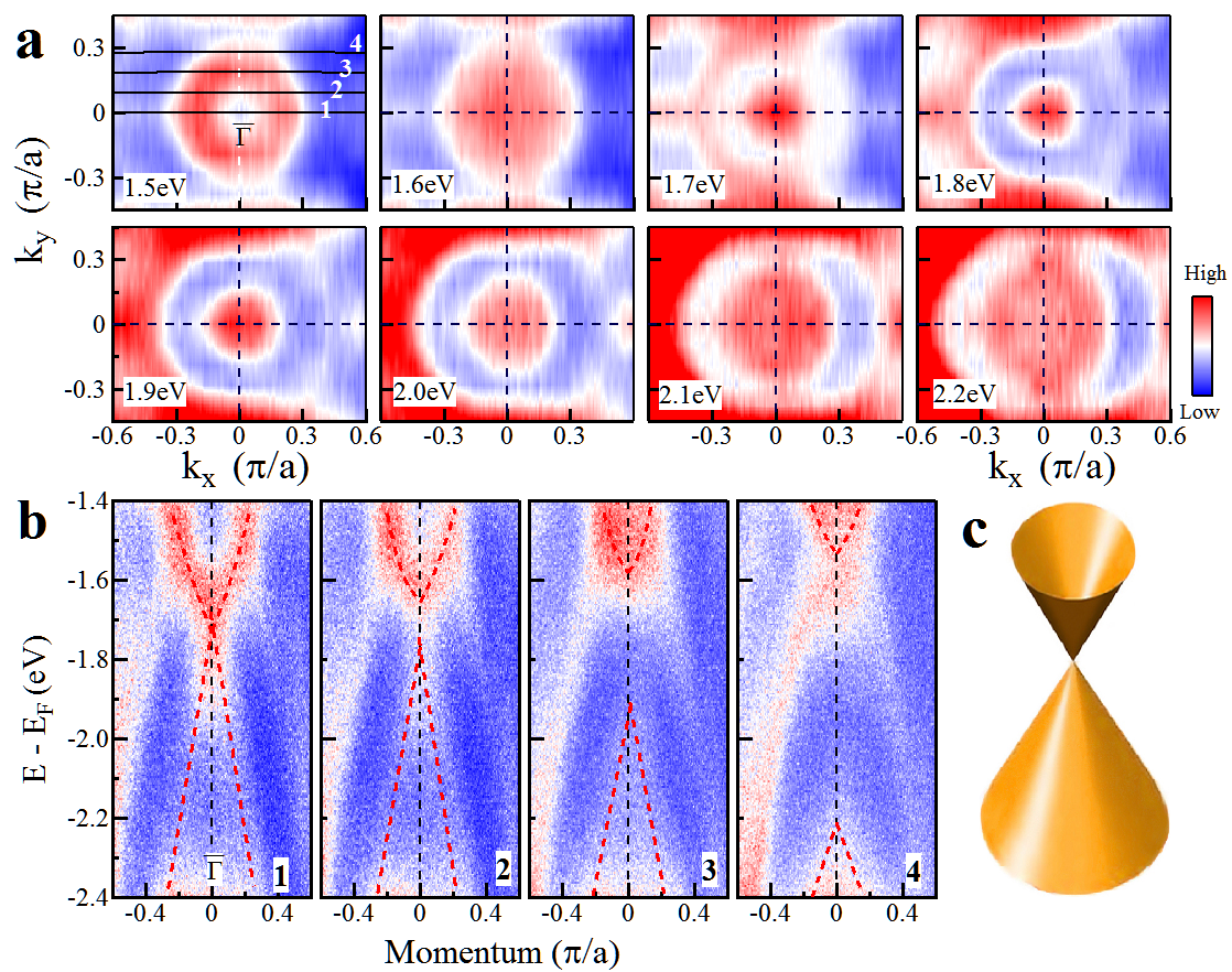
Figure 3 shows the measured constant energy contours at different binding energies for PdTe2 (Fig. 3(a)), as well as the momentum dependence of the band structures (Fig. 3(b)), near the Dirac point at a binding energy of 1.75 eV in the Brillouin zone center. The constant energy contours (Fig. 3(a)) evolve strongly with the binding energy, from a circular ring at 1.5 eV, to a smallest spot near 1.8 eV, and gets larger again and becomes a large circular ring at 2.2 eV. This is consistent with the typical behavior of a Dirac cone structure. Meanwhile, the momentum dependence of the band structure (Fig. 3(b)) also agrees with the Dirac cone picture. At the center point , it displayed two linear dispersion bands crossing at the Dirac point (1.75 eV)(Fig. 3(b), left-most panel). When moving away from the point, the bands gradually evolve into two parabolic-like bands without any intersection point. The upper band moves upward while the lower band shifts downward. All these findings provide strong evidence that this topological surface state possesses a typical Dirac-cone dispersion, as sketched in Fig. 3(c).
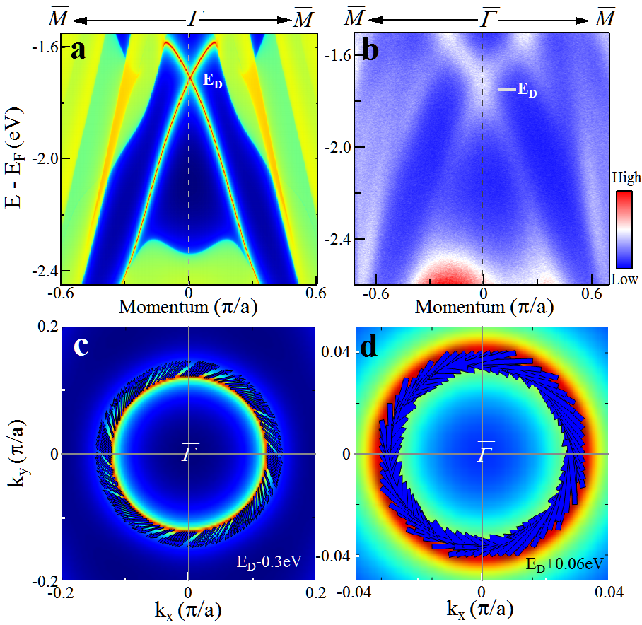
Figure 4 shows the topological surface state in PdTe2 and its spin texture. Fig. 4(a) zooms in on the theoretically calculated surface state and Fig. 4(b) compares the experimental data with the calculation. The experimentally observed Dirac point is at the binding energy of 1.75 eV and the agreement between the calculation and measurement is remarkable even in fine details. This surface state can be well-resolved because it stands out away from the bulk states, different from most of other surface bands that mix with the bulk bands. As one important character of the topological surface state, we have calculated the spin texture for the upper and lower Dirac cone branches. The spin texture for the lower Dirac branch is exemplified by the spin texture at 0.3 eV below the Dirac point in Fig. 3(c). The left-handed helical spin texture is expected for the lower Dirac cone branch. The spin texture for the upper Dirac cone branch is right-handed, as shown by the spin texture at an energy of 0.06 eV above the Dirac point (Fig. 4(d)). Such spin texture is similar to that found in usual three-dimensional topological insulators, and can be tested in the future spin-resolved ARPES measurements.
In summary, by combining high resolution ARPES measurements with theoretical calculations, for the first time, we have established PdTe2 superconductor as a new system that possesses topological surface state. The topological surface state in PdTe2 is at the Brillouin zone center and is well separated from the bulk states. It possesses helical spin texture similar to that in three-dimensional topological insulators. Compared with the usual topological insulators where the Dirac cone lies near the Fermi level, our results provide a new case where the topological surface state is realized in a pristine superconductor instead of a topological insulator, and the Dirac cone of the surface state lies well below the Fermi level (1.75 eV binding energy) instead of being at the Fermi level. Further work needs to be done to explore whether such a unique topological surface state well below the Fermi level and in a superconductor can lead to new phenomena, properties and applications. More work also needs to be done to investigate the nature of other surface states, particularly those crossing the Fermi level. The identification of topological surface state in PdTe2 also opens a door for searching for new topological materials in transition metal chalcogenide systems.
References
- (1) Hasan M Z and Kane C L 2010 Rev. Mod. Phys. 3045
- (2) Qi X L and Zhang S C 2011 Rev. Mod. Phys. 1057
- (3) Qi X L et al 2009 Phys. Rev. Lett. 187001
- (4) Qi X L and Zhang S C 2010 Phys. Today 33
- (5) Moore J 2009 Nat. Phys. 378
- (6) Qi X L, Hughes T L and Zhang S C 2008 Nat. Phys. 4 273
- (7) Li R, Wang J, Qi X L and Zhang S C 2010 Nat. Phys. 6 284
- (8) Qi X L, Li R, Zang J and Zhang S C 2009 Science 323 1184
- (9) Fu L and Kane C L 2008 Phys. Rev. Lett. 100 096407
- (10) Yu R et al 2010 Science 329 61
- (11) Majorana E 1937 Nuovo Cimento 171
- (12) Wilczek F 2009 Nat. Phys. 614
- (13) Xia Y et al 2009 Nature Physics 5 398
- (14) Zhang H J et al 2009 Nature Physics 5 438
- (15) Chen Y L et al 2009 Science 325 178
- (16) Hor Y S et al 2010 Phys. Rev. Lett. 104 057001
- (17) Wray L A et al 2010 Nat. Phys. 855
- (18) Moncton D E, Axe J D and DiSalvo F J 1977 Phys. Rev. B 16 801
- (19) Wilson J A, Salvo F J D and Mahajan S 1975 Adv. Phys. 24 117
- (20) Smaalen S V 2005 Acta Cryst. A61 51
- (21) Wilson J A and Yoffe A D 1969 Adv. Phys. 18 193
- (22) Finlayson T R 1986 Phy. Rev. B 33 2473
- (23) Roberts B W 1976 J. Phy. Chem. Ref. Data 5 581
- (24) Sipos B et al 2008 Nature Materials 7 960
- (25) Pyon S, Kudo K, and Nohara M 2012 J. Phys. Soc. Jpn. 81 053701
- (26) Yang J J et al 2012 Phys. Rev. Lett. 108 116402
- (27) Ali M N et al 2014 Nature 514 205
- (28) Cai P L et al 2014 arXiv:1412.8298 [cond-mat.mtrl-sci]
- (29) Ootsuki D et al 2013 J. Phys. Soc. Jpn. 82 093704
- (30) Ootsuki K et al 2014 J. Phys. Soc. Jpn. 83 033704
- (31) Ootsuki D et al 2014 Phys. Rev. B 89 104506
- (32) Novoselov K S et al 2005 Proc. Natl. Acad. Sci. USA 102 10451
- (33) Mak K F 2010 Phys. Rev. Lett 105 136805
- (34) Splendiani A 2010 Nano Lett. 10 1271
- (35) Radisavljevic B 2011 Nat. Nanotechnol. 6 147
- (36) Yoon Y, Ganapathi K, and Salahuddin S 2011 Nano Lett. 11 3768
- (37) Duerloo KA N, Li Y and Reed E J 2014 Nature Communications 5 4214
- (38) Zhang Y et al 2014 Nature Nanotechnology 9 111
- (39) Liu G D et al 2008 Rev. Sci. Instrum. 79 023105
- (40) Liu Y et al 2015 Chin. Phys. B 24 067401
- (41) Blaha P et al 2001 WIEN2k, An Augmented Plane Wave + Local Orbitals Program for Calculating Crystal Properties (Vienna: Vienna University of Technology).
- (42) McCarron E, Korenstein R and Wold A 1976 Mater. Res. Bull. 11 1457
- (43) Jobic S, Brec R and Rouxel J 1992 J. Solid State Chem. 96 169
- (44) Kim W S, Chao G Y and Cabri L J 1990 J. Less-Common Met. 162 61
- (45) Soulard C et al 2005 J. Solid State Chem. 178 2008
- (46) Jan J P and Skriver H L 1977 J. Phys. F: Metal Phys. 7 1719
- (47) Perdew J P, Burke K and Ernzerhof M 1996 Phys.Rev.Lett. 77 3865
- (48) Guo G Y 1986 J. Phys. C: Solid State Phys. 19 5365
- (49) Orders P J et al 1982 J. Phys. F: Met. Phys. 12 2737
Acknowledgement XJZ thanks financial support from the NSFC (11190022), the MOST of China (973 program No: 2011CB921703 and 2011CBA00110), and the Strategic Priority Research Program (B) of the Chinese Academy of Sciences (Grant No. XDB07020300).


