Space qualified nanosatellite electronics platform for photon pair experiments
Abstract
We report the design and implementation of a complete electronics platform for conducting a quantum optics experiment that will be operated on board a 1U CubeSat (a 10 x 10 x 10 cm satellite). The quantum optics experiment is designed to produce polarization-entangled photon pairs using non-linear optical crystals and requires opto-electronic components such as a pump laser, single photon detectors and liquid crystal based polarization rotators in addition to passive optical elements. The platform provides mechanical support for the optical assembly. It also communicates autonomously with the host satellite to provide experiment data for transmission to a ground station. A limited number of commands can be transmitted from ground to the platform enabling it to switch experimental modes. This platform requires less than 1.5W for all operations, and is space qualified. The implementation of this electronics platform is a major step on the road to operating quantum communication experiments using nanosatellites.
Index Terms:
photon entanglement, space-based quantum communication, CubeSat, nanosatelliteI Introduction
A number of proposals [1, 2, 3] have been been published for building global quantum communication networks using satellites that host quantum light sources or detectors. Efforts are underway to implement the first demonstrations. Together with collaborators [4, 5], we have proposed that nanosatellites (spacecraft that have a mass below ) have a role to play in this effort. They could act as demonstrators to raise the technology readiness level of essential components and also as the final platforms that transmit and receive single photons from ground-based stations or other satellites. In particular, we propose that nanosatellites can effectively host robust and compact sources of polarization-entangled photon pairs, which are the workhorse for entanglement-based quantum communication. The decreasing cost of launching a nanosatellite into low earth orbit has added impetus to this approach [6].
In order to use nanosatellites effectively, we are working to create small, low-resource and rugged photon pair sources that are fully compatible with the popular CubeSat standard [7]. The photon pair source that we are building is called the Small Photon-Entangling Quantum System (SPEQS), and it is an integrated instrument combining low-power electronics and a rugged optical assembly.
The SPEQS instrument is designed to produce and detect pairs of photons via a process known as spontaneous parametric down conversion (SPDC) [8]. In the SPEQS design a pump beam interacts with a nonlinear optical crystal. With some probability a pump photon is converted into a pair of daughter photons obeying energy and momentum conservation. The daughter photons are strongly correlated in polarization. Consequently, a measurement of the polarization correlation is a good mechanism for monitoring the performance of the entangled photon source. The aim of the first SPEQS instrument is to demonstrate that the precisely aligned SPDC source survives launch and can perform reliably in low Earth orbit. This performance will be monitored by measuring the quality of the polarization correlations.
The electronics platform for the SPEQS instrument must operate a number of opto-electronic devices efficiently. These include the diode laser for the pump beam, the Geiger-mode avalanche photodiodes (GM-APD) for detecting the downconverted photons and polarization rotators. In addition to the operation of the opto-electronic devices, the SPEQS instrument must store experiment data. Experiment data are primarily in the form of photo-detection events generated by the GM-APDs, and associated house-keeping data such as laser power and temperature. Data must be stored on the SPEQS instrument before transfer to the spacecraft bus for transmission to ground stations.
The platform also serves as the mechanical interface between the spacecraft and the optical assembly. In this paper, we report the design and implementation of the electronics platform that enables the SPEQS instrument to operate autonomously on board a 1U CubeSat.
II Main modules of the electronics platform
The electronics platform is designed around the Cypress CY8C3666 Programmable-System-On-Chip (PSoC3) microcontroller. The PSoC3 is widely used in white goods and is easily available as a commercial-off-the-shelf (COTS) component. The PSoC3 is essentially an 8-bit 8051 microcontroller bundled together with many digital components such as counters, timers, analogue-to-digital converters (ADC), digital-to-analogue converters (DAC) and pulse-width-modulation (PWM) devices. These active components are widely used for signal preparation and conditioning in quantum optics experiments, and it is convenient to access all these devices on a single chip. The functional blocks are configured using a development environment supplied by Cypress (PSoC3 Creator Integrated Development Environment).
With these available building block components, there is less need for external chips or glue-logic circuitry reducing the physical footprint of the platform. However, to enable complex analogue signal flows there is still the need for additional circuitry composed of an assortment of switch capacitors, op-amps, comparators, and digital filter blocks.

FIG. 1 illustrates the concept of operations (ConOps) after the platform is powered on by the satellite’s on-board computer (OBC). Upon activation, the platform receives a command code from the OBC that determines the experimental profile for the optical experiment. A heating mode is activated to bring the optical experiment within an acceptable temperature range. When the temperature range is achieved, the main opto-electronics components (GM-APD, pump laser, liquid crystal polarization rotator) are turned on sequentially. During the experiment, the heating mode is maintained. Upon conclusion of the experiment, data is stored on a memory module before transfer to the OBC.
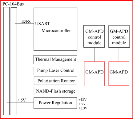
The main functional modules of the platform are shown in FIG. 2 With the exception of the power regulation module (implemented using COTS regulators), these modules will be described in the rest of this section. The GM-APD and polarization rotator modules will be presented in more detail, as they are relatively complex mixed digital-analogue circuits.
II-A GM-APD module
The GM-APD (Laser Components SAP500) used in the SPEQS instrument is a reach-through device with a large active area and relatively high detection efficiency whose breakdown voltage () is slightly above at room temperature. Under normal operating conditions the bias voltage () applied to a GM-APD is in excess of , and the photon detection efficiency is a function of this excess voltage ( = - ). When a photo-electron is present in the active area of the GM-APD an electron avalanche is generated and detected as a current pulse. From the pulse rate, the brightness of the entangled photon source is determined. Pairs of photons are identified via correlated pulses from two GM-APDs.


FIG. 3(a) shows the block diagram of the GM-APD module which incorporates a pulse detection method that uses a real-time feedback control loop. The control loop maintains a fixed in order for the detection efficiency to be constant over a range of operating temperatures ( changes with temperature).
The GM-APD is passively quenched which requires the current during an avalanche event to be below (the latch current). The current value is limited by using an adequately large quench resistor, , such that the value of / is smaller than the latch current of the given GM-APD. During quench, the bias voltage across the GM-APD falls below . The bias voltage then recovers to its nominal value exponentially with a time constant ( where is the inherent capacitance of the GM-APD plus parasitic capacitance). A typical parasitic capacitance is on the order of , while the inherent capacitance of a GM-APD is about putting the recovery time constant at approximately .
For each GM-APD, there is a pair of “top” and “bottom” sense resistors. The “bottom” sense resistor value is selected so that it produces an avalanche pulse whose peak voltage is half in value to that of the “top” sense resistor. Each pulse is compared against a constant level discriminator (CLD) to ensure that the ratio of bottom-to-top (BTR) pulses is maintained within a pre-calibrated range. When this range is exceeded, it is taken to mean that the bias voltage should be reduced. When the ratio falls below the range, the bias voltage is increased. This technique enables avalanche events to contribute to the bias voltage control and does not rely on temperature measurements.
A pulse-stretching circuit converts the output of the CLDs to be in duration, in order for the microcontroller to detect the pulses. Within the microcontroller, a 16-bit counter is configured to register and accumulate electronic pulses from each CLD. The counter accumulates its register value into a software variable every . Every second this variable is saved into a flash memory device as part of the experiment record.

The GM-APD is supplied with bias voltage from a regulated source (Matsusada TS-0.2P) capable of supply up to . For the temperature variation within a nanosatellite, it was determined that a tuning range for the bias voltage ( to ) was sufficient. It was also highly desirable to have the ability to tune the high voltage output in steps of in order to avoid over-shooting the optimal operating voltage. However, the microcontroller cannot directly provide such a high resolution over the entire range.
To achieve this, a “summing amplifier” circuit was constructed as illustrated in FIG. 3(b). A current DAC (iDAC) generates a current in steps of which is used to generate a variable voltage. A standard DAC is programmed to produce an offset voltage. A summing operational amplifier adds the offset voltage to the variable voltage and produces the final control voltage. This setup achieves a continuous control of the voltage source output with the required resolution.
II-B Polarization Rotator Module
To measure polarization correlations, it is necessary to analyse the polarization of the photons over an entire basis, for example in the linear basis. In a laboratory setup this is typically performed by rotating wave-plates mechanically. Amongst other problems, this introduces torque on a spacecraft, potentially interfering with its attitude control. To avoid this, we have implemented an inertial-free polarization rotator based on liquid crystal technology.
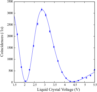
The liquid crystal polarization rotators (LCPRs) are customized for the target wavelengths ( and ). The polarization rotation responds to the amplitude of a DC-balanced square wave at generated by the PWM component of the microcontroller. The PWM output is logic fed into a dual digital potentiometer. The wiper positions of the potentiometer can be adjusted so that the final waveform amplitude sent to the LCPR can be adjusted in steps of . FIG. 4(b) shows the high contrast variation in the photon pair detection rate when one LCPR is supplied with fixed voltage, and the other LCPR has its amplitude adjusted between and (corresponding to a half wave plate rotation of approximately ). This high contrast indicates that fine control over polarization rotation can be achieved by the LCPRs.
II-C Pump laser, thermal management and NAND-Flash storage
The SPEQS optical unit contains a grating-stabilized GaN-based laser diode emitting at (Ondax CP-405PLR40). The laser diode is always operated as a continuous-wave device. For flexibility we implemented a module which can operate the laser diode in constant current mode or in constant power mode. This is illustrated in FIG. 5.

In constant power mode, an external Si PIN photodiode (Hamamatsu S5106) configured in reversed bias monitors the power of the pump beam in the SPDC process. As the SPDC efficiency is on the order of /mm, essentially all the laser power is picked up by the photodiode. The microcontroller samples the photodiode output periodically and adjusts the laser current, maintaining the power at the set point.
In constant current mode, the voltage across a sense resistor (Rs) is used to generate an error signal that is compared with a set value. A MOSFET switch is used to control the laser current in steps of . For a smaller current step size, the value of the sense resistor can be increased.
The optical assembly is always constructed at approximately and can operate on either side of this up to a range of . However, the nanosatellite thermal environment can oscillate between to [9], hence it is desirable to stabilize the temperature of the optical assembly. A heating module operates in two modes: “high” and “low”. The implementation is illustrated in FIG. 6.

In the “high” mode, a heating element (H) draws of power to rapidly raise the temperature of the optical assembly to within operating range. This mode will be used when the SPEQS instrument is powered on. Repeated testing under vacuum has shown that this mode can raise the optical assembly temperature by approximately per minute.
In the “low” mode, a secondary heating element (L) is added in series to H, drawing a maximum of . This is performed by selectively turning on a MOSFET switch. Testing has demonstrated that in conjunction with the heat generated by the pump laser, the temperature of the optical assembly can be maintained within the operating range.


Experiment data is stored on a 8-Mbit SPI-based NAND flash memory device with 16 sectors. Each sector of memory is 65536 bytes. To alleviate the possibility of corruption by radiation each set of record data is stored redundantly in two different sectors of the memory at intervals. Each frame of data is 32 bytes, and each page of memory is 256 bytes, allowing 7 frames of data to be written into each page. With this configuration it is possible to store up to of data in each sector.
III Discussion and Conclusion
The form-factor of the electronics platform is designed to conform to the CubeSat design specification [10]. The printed circuit board housing the electronics measures x . With the optical assembly mounted, the overall height of the package is 38 mm, and the entire instrument mass is less than . The electronics platform incorporates a stackable PC-104 bus for power and signal connections with the rest of the spacecraft. The electronics platform is also relatively efficient in power consumption, and in experiment mode (running a pump laser and two high-efficiency GM-APDs), consumes less than (see TABLE I). We anticipate future power savings when a large number of the electronic operations are moved into integrated devices such as complex programmable logic devices (CPLDs) or field programmable gate arrays (FPGAs). This migration into software-defined circuits could further reduce design complexity while improving system robustness.
| Electronics Platform Sub-Systems | Power Consumption (W) |
|---|---|
| Thermal Management (High)* | 2.5 |
| Thermal Management (Low) | 0.4 |
| GM-APD Control | 0.24 |
| Pump Laser Management | 0.45 |
| LCD Polarisation Rotator | 0.1 |
| PsoC3 Operation @ 24MHz (Normal) | |
| -Computation, Data Storage, | |
| USART Communications | 0.3 |
| PsoC3 Operation (Standby) | 0.1 |
The electronics platform has been tested successfully in radiation [11], thermal-vacuum and vibration environments to simulate launch and operation in space. Further testing in a near-space environment using a high altitude balloon [12] was also successful. The first attempt at putting a SPEQS experiment into orbit occurred in 2014 when the instrument was integrated onto the GomX-2 satellite (see Appendix A) that was lost in a launch vehicle failure. Because the SPEQS experiment has followed the CubeSat standard, it has been accepted on other CubeSat missions. Performance data from low Earth orbit is expected to be available in early 2016.
We have presented the main blocks of an electronics platform that can support the operation of an entangled photon source on a 1U CubeSat. The concept of the integrated electronics platform for supporting space-based quantum communications has been demonstrated, and the design will be utilised in future SPEQS-based missions.
Acknowledgment
During the development of this platform, C. Cheng and Tan Y. C. were supported by the DSO-CQT project on quantum sensors. Both of them are currently supported by the National Research Foundation project NRF-CRP12-2013-02. The authors thanks R. Bedington for assistance with the manuscript.
Appendix A

References
- [1] R. Ursin et al., “Space-quest, experiments with quantum entanglement in space,” Europhysics News, vol. 40, no. 3, pp. 26–29, 2009.
- [2] T. Scheidl, E. Wille, and R. Ursin, “Quantum optics experiments using the International Space Station: a proposal,” New Journal of Physics, vol. 15, no. 4, p. 043008, Apr. 2013.
- [3] T. Jennewein, C. Grant, E. Choi, C. Pugh, C. Holloway, J. Bourgoin, H. Hakima, B. Higgins, and R. Zee, “The NanoQEY mission: ground to space quantum key and entanglement distribution using a nanosatellite,” vol. 9254, p. 925402, Oct. 2014.
- [4] W. Morong, A. Ling, and D. Oi, “Quantum optics for space platforms,” Optics and Photonics News, no. October, pp. 42–49, 2012.
- [5] A. Ling and D. Oi, “Small Photon-Entangling Quantum Systems (SPEQS) for LEO Satellites,” in Proc. International Conference on Space Optical System and Applications (ICSOS), vol. 12. Ajaccio: ICSOS, 2012.
- [6] J. Coopersmith, “The cost of reaching orbit: Ground-based launch systems,” Space Policy, vol. 27, no. 2, pp. 77–80, May 2011.
- [7] K. Woellert, P. Ehrenfreund, A. J. Ricco, and H. Hertzfeld, “Cubesats: Cost-effective science and technology platforms for emerging and developing nations,” Advances in Space Research, vol. 47, no. 4, pp. 663–684, Feb. 2011.
- [8] D. C. Burnham and D. L. Weinberg, “Observation of simultaneity in parametric production of optical photon pairs,” Phys. Rev. Lett., vol. 25, pp. 84–87, 1970.
- [9] J. Kataoka et al., “In-orbit performance of avalanche photodiode as radiation detector on board the picosatellite cute-1.7+apd ii,” Journal of Geophysical Research, vol. 115, no. A5, p. A05204, May 2010.
- [10] S. Lee, A. Hutputanasin, A. Toorian, W. Lan, and R. Munakata, “CubeSat design specification,” The CubeSat Program, vol. 8651, p. 22, 2009.
- [11] Y. C. Tan, R. Chandrasekara, C. Cheng, and A. Ling, “Silicon avalanche photodiode operation and lifetime analysis for small satellites.” Optics express, vol. 21, no. 14, pp. 16 946–54, Jul. 2013.
- [12] Z. Tang, R. Chandrasekara, Y. Y. Sean, C. Cheng, C. Wildfeuer, and A. Ling, “Near-space flight of a correlated photon system.” Scientific reports, vol. 4, p. 6366, Jan. 2014.