Characterization of carrier transport properties in strained crystalline Si wall-like structures as a function of scaling into the quasi-quantum regime
Abstract
We report the transport characteristics of both electrons and holes through narrow constricted crystalline Si “wall-like” long-channels that were surrounded by a thermally grown SiO2 layer. The strained buffering depth inside the Si region (due to Si/SiO2 interfacial lattice mismatch) is where scattering is seen to enhance some modes of the carrier-lattice interaction, while suppressing others, thereby changing the relative value of the effective masses of both electrons and holes, as compared to bulk Si. Importantly, as a result of the existence of fixed oxide charges in the thermally grown SiO2 layer and the Si/SiO2 interface, the effective Si cross-sectional wall widths were considerably narrower than the actual physical widths, due the formation of depletion regions from both sides. The physical height of the crystalline-Si structures was nm, and the widths were incrementally scaled down from nm to nm. These nanostructures were configured into a metal-semiconductor-metal device configuration that was isolated from the substrate region. Dark currents, dc-photo-response, and carrier “time-of-flight” response measurements using a mode-locked femtosecond laser, were used in the study. In the narrowest wall devices, a considerable increase in conductivity was observed as a result of higher carrier mobilities due to lateral constriction and strain. The strain effects, which include the reversal splitting of light- and heavy- hole bands as well as the decrease of conduction-band effective mass by reduced Si bandgap energy, are formulated in our microscopic model for explaining the experimentally observed enhancements in both conduction- and valence-band mobilities with reduced Si wall thickness. The role of the biaxial strain buffing depth is elucidated and the quasi-quantum effect for the saturation hole mobility at small wall thickness is also found and explained. Specifically, the enhancements of the valence-band and conduction-band mobilities are found to be associated with different aspects of theoretical model.
pacs:
PACS:I Introduction
For over 40 years the microelectronics market place has driven the very large scale integration (VLSI) industry to make continuous improvements in computational power, bandwidth and speed. add1 These continued enhancements in performance have come in the form of “cramming” more components onto integrated circuits, as was predicted in 1965 by Gordon E. More. add2
The push to increase the speed and density of the transistors on a chip has come in the form of shrinking the transistor size, in particular the channel length. add3 ; add4 However, reductions in channel length have come with challenges i.e., short channel effects. add5 Short channel effects lead to higher leakage currents, poor signal-to-noise ratios and instability during operation, such as loss of channel’s gate control.
In order to improve the transistor’s gate control and switching speed, the contemporary metal oxide semiconductor (CMOS) industry has looked for alternative solutions to the traditional planar transistor designs and substrates. add6
Over the past several years, the CMOS industry has narrowed their focus into multi-gate field effect transistor designs add7 for improving the gate control, and strained substrates add8 ; add9 to enhance carrier carrier mobilities and ultimately the switching speed and drive currents.
One particular multigate transistor design that has gained considerable interest among the industry, as a replacement for the planar design, is the FinFET add7 . The FinFET has a tri-gate architecture and reductions of short-channel effects have been observed in these devices. add10 ; add11 This design provides gate control, not only from the top of the channel, but also from the channel sides as well. This in itself improves the overall (on/off) gate control process, however, the drawback is that these devices require higher operating voltages to achieve faster switching speeds. add12 S. W. Bedell et. al., r7 has reported that in the present FinFET technologies, the carrier mobilities are not seen to be enhanced, since the active region of these devices would require two opposite kinds of strain (i.e. tensile and compressive) on the same substrate, which would be possible by converting the tensile strain of silicon-on-insulator substrates to compressive strain in localized regions via a combination of selective SiGe() growth. Such FinFET devices have not yet been experimentally demonstrated. However, similar embedded silicon/germanium layered structures that would provide process induced stressors in the source and drain regions have been theoretically modeled. The results of these simulations show only a modest performance increase, approximately one-half enhancement in mobility, as compared to similar size planar FETs. sun Process induced strain in a FinFETs would be most effective if it was directly under the gate region, as its stressor’s effectiveness diminishes with depth. Incorporation of wafer level strain using SiGe-on-insulator (SGOI) and Strained Silicon-On-Insulator (sSOI) in small pitched circuits may be possible by converting the tensile strain of sSOI to compressive strain by selective growth of silicon-germanium. However, these type of configurations would certainly add complexities in a high volume manufacturing environment, which could negatively affect yield.
In this paper we report an comprehensive experimental and theoretical study on the nature of carrier transport, of both electrons and holes, through narrow constricted crystalline Si “wall-like” long-channels that were surrounded by a thermally grown SiO2 layer. The carrier transport characteristics are evaluated as a function of dimensional scaling of the Si wall widths from nm to nm. The Si wall-widths were reduced by the process of thermal oxidation, where stress naturally accumulates in the channel. Basically, this structure configuration allows us to investigate the effects of strained regions that are “closing-in” from both sides. Additionally, as the wall-widths approach the quasi quantum regime, the carriers start to become confined and therefore react to the narrow paths, and possibly behave more like waves then particles, add15 thus altering the macroscopic nature of resistance, capacitance and inductance to a more exotic microscopic one. add16 However, this transition into the quantum mechanical regime does not come about abruptly. Rather, there is a transition region in which the bulk properties begin to slowly weaken while the quantum effects begin to strengthen.
The effects of quantum confinement on carrier transport properties, however, have been primarily investigated in ternary and quarternary material heterostructures and supperlattices, in which scattering is seen to enhance some modes of the electron-lattice interactions while suppressing others, thereby changing the relative value of the carrier’s effective masses of electrons and holes, as compared to bulk semiconductors. r4 To date such studies in Si have been very limited. We believe that these wall structures are a useful starting point for a broader study, as these can be configured into novel high density 3-D VLSI devices, where thermal effects, such as heat buildup, can also be efficiently managed. add18
We organize the rest of the paper as follows: In Sec. II the process for fabricating the crystalline Si wall structures is described, and the two electrode, metal-semiconductor-metal device structure fabrication is also discussed. In Sec. III, the experimental dc measurements as a function of wall width thickness are presented, including dark currents and photocurrents.
II Fabrication
II.1 Rationale for substrate material
Silicon-on-insulator (SOI) wafers with a top active layer of crystal orientation were used to fabricate the wall-like structured devices for this study. The initial SOI structure had a nm active layer on top of a nm buried oxide. The SOI configuration allowed complete electrical isolation of the Si wall-like structures from the underlying substrate. All five samples in this study had identical -type active layer with a lightly doped concentration of cm-3 boron atoms. Intrinsic SOI wafers would have been an ideal choice for the experiment; however, due to the commercial unavailability of intrinsic material, the above choice of dopant type and concentration was adequate enough to minimize the effects of impurity scattering. Boron tends to segregate away from the Si interface and into the thermally grown oxide add19 , thus reducing the impurity concentration near the Si interface with SiO2. Thus the segregation coefficient, which is defined as the ratio of the dopant concentrations at the interface, is less than one in our case. The thermal oxidation process leads to the formation of an oxide trapped charge (), which contribute to the formation of a depletion region near the Si/ SiO2 interface. r9 ; r10 Now, if we combine this oxide trapped charge with the fixed charge () which naturally results from the excess Si atoms not reacted with the oxygen, and the interface trapped charge () which results from the mismatch between the number of atomic bonds in the Si crystal surface and the number of available bonds in the SiO2 layer, these all sum to (). Combined these form an depletion region in Si that extends several nanometers away from the SiO2 interface. r10 ; r11 Thus the effective Si cross-sectional wall widths were considerably narrower than the actual physical widths, due this formation of depletion regions from both sides.
II.2 Crystalline silicon wall nanostructure fabrication
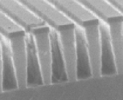
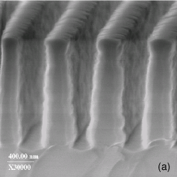
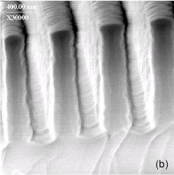
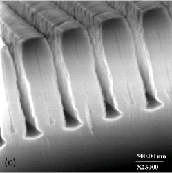
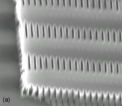
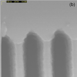
In order to fabricate the wall structures, photoresist nano-scale pattering was required. The precursors to the wall structures were patterned using interferometric lithography (IL) r15 and reactive-ion-etching (RIE) add24 ; add25 . IL is a well-developed technique for inexpensive nano- patterning process. add26 IL, in its simplest form, is interference between two coherent waves resulting in a 1-D periodic pattern defined by where is the optical wavelength and is the angle between the interfering beams. A typical IL configuration consists of a collimated laser beam incident on a Fresnel mirror (FM) arrangement add27 mounted on a rotation stage for period variation. There is no -dependence to an IL exposure pattern, which is limited only by the laser coherence length and beam overlaps add28 . The 1-D nanoscale patterns were first formed in the photoresist followed by pattern transfer onto the underlying substrate using RIE in a parallel plate reactor using SF6 plasma chemistry. Figure 1 shows a scanning electron microscope (SEM) cross-sectional image of an array of nano-wall structures with a remaining layer of patterned photoresist after RIE has been performed. Note at this stage these structures are merely the precursors to the thin Si wall structures that are then reconfigured into metal-semiconductor-metal (MSM) devices. After the photoresist was re- moved, the wall structures are thermally oxidized. The oxidation process accomplished two things. First, it consumes the Si, thus thins the wall width. Secondly, the thermally grown oxide preserves a low defect, clean Si/SiO2 interface, and at the same time passivates the surfaces of the nanostructures. r15 ; r16 The Si/SiO2 interface has low defects and it is important to note that strain is present at the interface and it reduces with distance from the interface. This reduction in strain as a f unction of depth has been seen experimentally in Si/SiO2 interfaces using a scanning transmission electron microscope using Z-contrast imaging which produces strain contrast imaging r18 . Using this technique, the decay length was measured at approximately nm. The modeling of the thermal oxidation parameters needed for the desired thicknesses was complicated due to the f act that in a three dimensional wall structure there are several crystal lattice orientations that have different thermal oxidation rates. As a first order approximation, we used average values of oxidation rates between the various lattice orientations i.e. oxygen ow rate, pressure, temperature and time. These parameters were then fine-tuned empirically during the actual thermal oxidation runs. Figure 2(a)-2(c) show SEM images of the cross-sectional views of the wall structures after the respective thermal oxidations. As can be seen from the SEM images, due to the high aspect ratio of these structures the oxidation rate was not fully uniform throughout the height of the walls. The rate was faster at the top part of the walls and slower at the bottom part due to higher availability of oxygen atoms in the upper regions. The resulting wall-like Si structures surrounded by the thermally grown oxide are then configured into the active region of the MSM devices as described in the next section.
II.3 MSM device fabrication
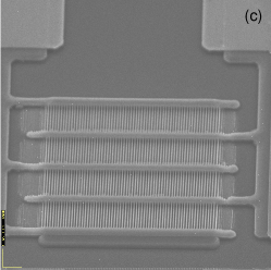
The wall structured samples were then configured into two terminal metal-Si/nanowall- metal (MSM) devices for optical and electrical characterization. The MSM device configuration was specifically designed so the current would ow within the wall boundaries between the electrodes. This allowed the physical cross-section of the wall structures to dictate the current flow properties. The mesa structures were fabricated to cutoff any stray current paths that could bypass the intended active region (wall) carrier path. Figure 3(a) shows a SEM picture of a typical pre-device mesa structure. After the walls were oxidized to achieve the desired wall width, the thermally grown oxide was selectively removed from the planar un- textured Si pad locations [Figure 3(b)] using an appropriate photo-mask and a chemical buffered oxide etch (BOE) process.
Following the resist removal the samples were cleaned using a sulfuric-acid/hydrogen-peroxide solution, and a DI water rinse followed by a nitrogen gas dry step. The samples were then re-patterned using photoresist and a second mask was used in the process to form the electrode contact regions. Three separate evaporations (30 nm of Ni) were performed. The first one was performed at a normal incidence to the sample surface and the other two at a degree tilt angles in order to ensure complete coverage of the mesa step height. After Ni evaporation, liftoff was performed to remove the unwanted metal and resist using acetone. Following a thorough clean using methanol/DI-water, the samples were again dehydrated and spin-coated with a thick resist layer. The samples were patterned using a final metallization mask set. A layer of Cr and Au was evaporated on the electrode regions. nm/ nm of Cr/Au were evaporated and liftoff process was used to remove the resist and unwanted metal. Figure 3(c) shows SEM pictures of a fully fabricated wall device.
III Electrical and Optical Measurements and Analysis
III.1 DC measurements
At room temperature only a small number of carriers are thermally generated (as dark current) for a Si bandgap of eV. At low bias voltages (linear region of operation) the slope of the - dark current is proportional to the device resistance that includes contributions of thermally generated carriers from both the wall channels and the metal/semiconductor contact regions. At higher biases the current saturates when all thermally generated carriers are collected. Any further increase in the current can be attributed to leakages across the contact metal-semiconductor barrier and to non-linear generation of carriers across the barrier. r17 The back interpolation of this leakage current to the zero bias ( V) is a measure of the saturated dark current (). Although the photocurrents are a few orders of magnitude larger than the thermally generated dark currents, the analysis of the photocurrent () function is the same as the dark current () plots. For dc response analysis, two sets of measurements were performed. These include: (i) dark currents as a function of wall width thickness, and (ii) photocurrents as a function of wall width thickness. These results are discussed and analyzed below.
III.2 Dark currents versus wall width thickness
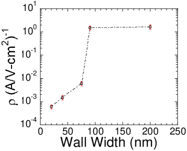
To study the carrier conduction properties versus dimensionally scaling down the width of the wall structures into the nano-regime, the samples were characterized in batches. Using samples with wall widths of nm, nm, nm, nm, and nm, the room temperature dark currents were measured with a probe station and digital - curve tracer. As the physical cross-sectional area of the wall widths was reduced from nm to nm, we know from Ohm’s law, the resistance should increase linearly as a function of area. In other words the resistivity in units of should remain constant. However, as can be seen from the Figure 4, the resistivity is not constant but drops significantly as the width of the wall is reduced below nm. This suggests that there is an increase in conductivity as the wall thickness decreases from nm to nm. Since the number of thermally generated carriers is directly proportional to the volume of the active region, any increase in the conductivity, as wall width cross-sectional region decreases from nm to nm, cannot be attributed to the volume of the semiconductor material, but must be the result of a substantial increase in the carrier velocity. Confirmation of this hypothesized mechanism was obtained with the use of transient time analysis as discussed in subsection III.4.
III.3 Photocurrents versus wall width thickness
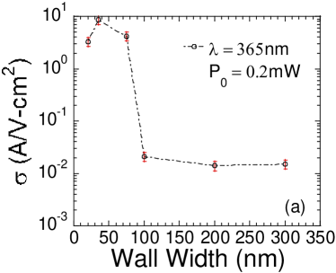
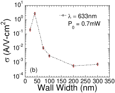
DC steady state photocurrents were measured using a nm wavelength, W argon-ion laser and a nm wavelength, W HeNe laser. The laser beam spot diameter was less than m and was focused within the active region of the electrode spacing covering several wall structures. By using nm and nm wavelengths, a more complete insight into absorption and carrier transport as a function of wall thickness can be achieved. At nm, absorption occurs within the top first nm of the Si wall structures with heights of nm. For nm the total photon absorption extends through the entire wall height. Figure 5(a) and 5(b) show the conductivity versus wall thickness profiles respectively. As can be noted from the figures, a peak in the conductivity occurs around the nm (physical wall width) samples followed by a decrease around nm width samples. The significance of this can be explained through the effects of strain inside the wall structures that affect the carriers mobilities as the dimensions are reduced, as discussed in section IV.
III.4 Transient time response measurements and analysis
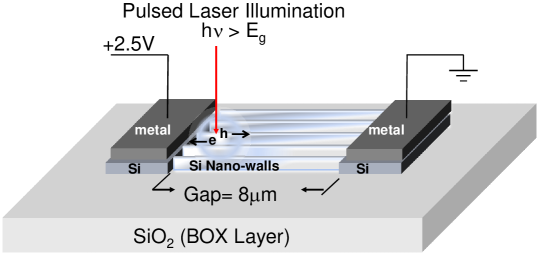
The schematic of the pulsed carrier transport experiment is shown in Figure 6. This setup is based on a modified version of the Haynes-Schockley r21 experiment. This measurement provides an unambiguous direct measure of the actual transit time of electrons and holes through the channel. When a narrow pulse of light strikes the wall structured active region of the device near the left electrode as shown in Figure 6, equal number of electrons and holes are generated, and are then subjected to diffusion and drift forces in a presence of an electric field. Based on the experimental configuration the electrons will be rapidly collected near the positively biased electrode and the holes will have to travel the entire channel to the negatively biased electrode. From the measured time response signal profile at the opposite electrode, the hole transient time limited carrier velocity can be determined, provided the carrier lifetime is greater than the total transit time. If the optical pulse of light strikes near the opposite electrode, the holes will be rapidly collected and the electrons would have to transit through the channel, thus the measured signal at the opposite electrode would be electron transit time limited.
The pulsed response measurements were taken using a -fs duration excitation at nm from a cw mode-locked Ti:Al2O3 laser (doubled for the short wavelength, mW average power at a MHz repetition rate).
The wall structured MSM devices were probe tested using an GHz probe and a high-speed digital sampling oscilloscope with an approximately ps resolution capability. The laser spot size was m in diameter and the electrode gaps were m. Normal incidence was used for the experiment. The time response measurements were taken for low electric field strengths Vcm, ( V across m gap) thus avoiding velocity saturation.
Before the experimental data and analysis is provided it is useful to review the three
primary factors that can impact the carrier transport through a semiconductor region. These factors are:
-
•
Field dependent velocity of carriers through the active region. At high -fields, the velocities of both electrons and holes in Si saturate at about cms,
,add19 provided the field within the electrodes exceeds the saturation value for most of its length, we can assume that the carriers move with a average velocity drift. Velocity saturation is not an issue in our experiment since the applied field is much lower than what is required for saturation. -
•
Diffusion of carriers in the active region. The time it takes for carriers to diffuse a distance is where is the carrier diffusion coefficient. The diffusion of carriers becomes a two dimensional process as the thickness of the Si wall-structures is reduced and carriers are physically constricted in movement by the Si/SiO2 interfaces from all sides.
-
•
Junction and parasitic capacitance effects. A metal-semiconductor junction under reverse bias exhibits a voltage-dependent capacitance caused by the variation in stored charge at the junction represented by the relation , where is the junction cross-sectional area, is the ionized donor density, is the dielectric constant and is the junction voltage. This capacitance is usually quite small for MSM device structures as a result of their planar electrode design. There are also parasitic circuit capacitances associated with the probing and cabling that usually dominate the electrical response as well as the limiting response of the electronics. For this study all film devices have an identical circuit limitation.
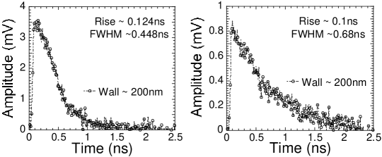
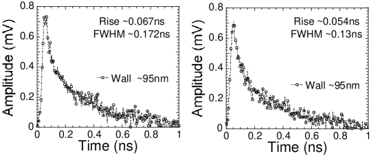
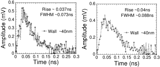
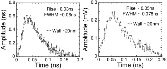
Figure 6 shows the bias polarity of our experiment in which the left electrode polarity is positive and the right electrode is ground. With this bias configuration once a pulse of light with a spot size m, as in the case of our experiment, strikes within the active region, the holes travel towards the right electrode and the electrons travel in the opposite direction towards the left electrode. Figure 7(a)-7(d) shows the experimental results of the time response measurements for nm, nm, nm and nm thick wall devices for both electron and hole dominated signals. From a first pass, as can be seen from these plots, as the thickness of the wall-channels are decreased, the time response signal decays faster. In particular in the case of the nm and nm thick walls the signal decays over an order of magnitude faster then the nm sample for both electrons and holes. The rise time of the signals is an important parameter, since it directly provides the carrier transit time. grundmann The rise time () is defined as is the time-lapse from moment when the pulse of light strikes one end of the active region of the MSM, near one electrode, and the moment when the photo-generated carrier signal is detected at the opposite electrode. From the rise time data, provided on Fig. 7(a)-7(d), we can determine the carrier mobilities as a function of wall thickness as follows. grundmann
First from the experimental time response measurements we can calculate the average carrier velocities by applying the given relation,
| (1) |
where is the average time it takes for the pulsed carrier signal to cross the electrode gap distance. The pulse travels in the presence of a field and expands from its originating point due to diffusion. In this case we are ignoring the RC time delay that the pulsed signal experiences once it reaches the edge of the depletion region near the electrodes since the widths of the depletion regions are very small in the sub-micron range compared to the electrode gap which is m in length.
By definition the average carrier mobility can be written as,
| (2) |
where is the external bias applied to the electrodes.
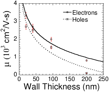
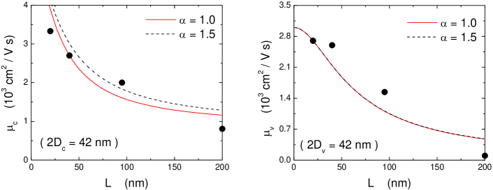
Figure 8 shows a plot of average field dependent electron and hole limited mobility values using experimental values of rise time, , and the above expression as a function of wall thickness. We know that the carrier transport of electrons and holes in the thickest wall sample ( nm) is essentially similar to the transport properties in bulk silicon. However we observe a considerable increase in low field dependent mobility values below nm wall thicknesses. Recall the fact that we actually have a much narrower effective cross-sectional regions from which carriers propagate due to the repulsive nature of the boundary at the Si/SiO2 interface, and the carrier profile tends to peak a certain distance away from the interface close to the center of the wall structures. r10 At these nanoscales we must account for the strain effects, which include the reversal splitting of light- and heavy- hole bands as well as the decrease of conduction-band effective mass by reduced Si bandgap energy. These strain effects are formulated in our microscopic model for explaining the experimentally observed enhancements in both conduction- and valence-band mobilities with reduced Si wall thickness, i.e. consider the case where the hole mobility is given by , where . The narrower light-hole band dominating the transport can have a significant enhancement on the overall mobility which is consistent with our experimental result. Specifically, the enhancements of the valence-band and conduction-band mobilities are found to be associated with different aspects of physical mechanisms. The role of the biaxial strain buffering depth is elucidated and its importance to the scaling relations of wall-thickness is reproduced theoretically. A detailed theoretical model is described in the next section which explains our experimental results in a comprehensive manner.
IV Strain Effects Modeling to Explain the Rise in Electron and Hole Mobility
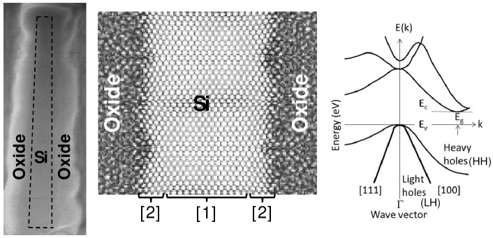
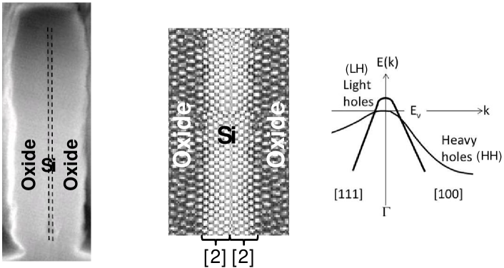
Figures 9(a)-9(c) represent the thickest wall channels and Figures 10(a)-10(c) represent the thinnest wall channels. Note that the associated E-k diagrams of Fig. 9(c) and Fig. 10(c) represent the center regions of the wall channel structures where the carriers flow through.
If we consider a total valence-band hole concentration then, the light-hole () and the heavy-hole () concentration will satisfy the charge-conservation relation , where
| (3) |
Here, the subscript takes HH or LH and the upper (lower) sign corresponds to HH (LH) state. In the above expressions, the approximations are made for high temperatures, is the volume of the silicon film, is the system temperature, the zero energy is chosen at the middle point between the split pair of light-hole and heavy-hole bands, is the three dimensional wave vector of carriers, (not due to strain effect) is the -valley degeneracy for holes and is the spin degeneracy for both light-holes and heavy-holes. In addition, , which depends on both and , is the chemical potential to be determined for valence bands, is the kinetic energy of heavy holes and is the kinetic energy of light holes, where and ( is the free-electron mass) are the effective masses for heavy holes and light holes, respectively. Additionally, introduced in the above expressions stands for the half of the valence-band splitting due to the existence of strain.
From Eq. (3) and , we obtain and , where . For biaxial and shear strains grundmann ; bahder , we have the valence-band splitting, given by , where the upper sign is for the compressive strain while the lower sign for the tensile strain in the direction perpendicular to the interface of silicon and silicon-dioxide materials, and are the optical deformation potentials, and represents the strain tensor in the three dimensional space with , and , the diagonal matrix elements are associated with biaxial strain, and the off-diagonal matrix elements with correspond to contributions from the shear strain. For silicon crystals, we have eV and eV.
If we choose the direction as the direction perpendicular to the interface for biaxial strain we simply get schaffler , , and for , where , . Moreover, the perpendicular lattice constant is related to the parallel lattice constant by , where N, and N are the elastic constants of silicon. For silicon and silicon-dioxide, we have Å and Å for amorphous silicon-dioxide materials. Therefore, we obtain . This leads to (compressive), (tensile), and .
The total mobility for holes can be expressed as sun
| (4) |
where and (for details of calculating hole scattering time, see Appendix A). comes from the mobility saturation effect, is the quasi-quantum confinement width, corresponds to the hole mobility in the absence of strain for , and are the scattering times for light holes and heavy holes, respectively. Moreover, the factor introduced in the definition of is given by , where is the maximum of the hole mobility in the limit of . It is clear that increases with decreasing for the tensile strain () in the direction perpendicular to the interface of silicon and silicon-dioxide materials, as observed by us in Fig. 11.
The values of introduced in Eq. (4) can be scaled as , where is the film thickness and represents the average spatially-dependent strain due to lattice mismatch between embedded Si crystal and surrounding amorphous SiO2 material at their interface, and represents the film effective thickness for unstrain part r25 . The scale of interest for these calculations of the effects of strain near a Si/SiO2 interface of a silicon nanowire was studied using molecular dynamics by Ohta, et. al. r26 . In this study, strain was most pronounced within - nanometers of the interface, tensile in the direction (perpendicular to the substrate) and compressive in the direction parallel to the substrate resulting in form of biaxial strain.
For a given conduction-band electron concentration , the electron chemical potential , which depends on both and , is decided from
| (5) |
where the high-temperature approximation is made in the above expression, is the bandgap energy of strained silicon crystals, which depends on and the hydrostatic part of the strain, stands for the bandgap energy of unstrained silicon crystals, (not due to strain effect) represents the (in direction) or (in direction) valley degeneracy for electrons at the two minima of conduction band, is the kinetic energy of electrons and is the transverse effective mass of conduction-band electrons with and . The dependence of (based on the Bose-Einstein phonon model) is given by grundmann , where eVK is a coupling constant, is a typical phonon energy with K, eV and eV at K for the X and L valleys. Moreover, the strain part of the bandgap energy is calculated as grundmann , where and are the deformation potentials of the conduction band for an indirect-gap silicon crystal ( eV, eV for the X valley and eV, eV for the L valley), eV is the difference of the deformation potentials of conduction and valence bands at two different valleys due to hydrostatic component of the strain for the silicon crystal, and is the unit vector pointing to the specific X or L valley. It is clear from the above equation that for the tensile strain and X or L.
The change in the bandgap energy by strain also affects the effective mass of conduction band, given by cardona
| (6) |
where we have neglected the shear strain and assumed a weak strain with , meV is the spin-orbit splitting and eV is the Kane energy parameter.
The total mobility of conduction-band electrons is obtained as
| (7) |
where comes from the mobility saturation effect, , , corresponds to the electron mobility in the absence of strain for , represents the scattering times of conduction-band electrons at two different valleys and the high-energy valley has been assumed depopulated, and (for details of calculating electron scattering time, see Appendix A). In addition, for electrons has the similar meaning of for holes. It is clear that the electron mobility is increased for , as oberserved by us in Fig. 11.
Our numerically calculated results for electron () and hole () mobilities are presented in Fig. 11, along with their comparisons with our experimental data. In our model calculations, we have taken K and the other model parameters can be found from Tables 1 and 2. The good agreement between our numerical calculated results and measured data strongly support the physical modeling present in this section.
V Summary and Conclusion
The semiconductor processing, fabrication and the resulting carrier transport characteristics of MSM devices fabricated as wall like structures in silicon on insulator technology were reported. MSM device dark current, DC photocurrents, and the time response of carrier transport were investigated. The resulting conducting channels were actually smaller than their physical dimensions, a result of depletion of carrier near the interfaces. As the physical channel widths were reduced by oxidation, strain was produced near the interface and strained lattice became a significant portion of the conducting channel. The increase in mobilities for both holes and electrons stemming from the strained silicon resulted in a dramatic increase in carrier mobility for both electrons and holes as the physical channel width was reduced from nm to nm. The theoretical model incorporating the effects of strain present in these nanoscale MSM devices compared favorably with experimental results, showing that hole mobilities increased with decreasing . Additionally, if these electron and hole mobilities can be retained with the application of gate electrodes, then this technique may yield a much simpler path towards high performance CMOS, both -channel and -channel, than current techniques for either planer ultra-thin body FETs or FinFETs.
Acknowledgements.
The authors would like to acknowledge the Air Force Research Laboratory, Space Vehicles Directorate for their support and interest in this work.Appendix A Carrier Scattering Time
In general, the carrier concentration includes both the doping and photo-excitation contributions. If the sample is undoped, we can simply neglect the impurity scattering and have . The optical-phonon scattering and the inter-valley scattering are only important at high temperatures, while the acoustic-phonon scattering becomes more important at low temperatures. laux The surface-roughness scattering, on the other hand, is largely independent of temperature.
For the impurity scattering, by using the Fermi’s golden rule, its scattering rate is calculated as huang1 ; huang2
| (8) |
where is the total number of carriers in the system, is the impurity concentration, is the impurity charge number, is the silicon dielectric constant, at high temperatures with , is the carrier kinetic energy, and stands for the carrier effective mass. For this case, we have . In addition, at high temperatures we get conduction-band electron distribution
| (9) |
where we have assumed the high-energy valley becomes depopulated. Similar results can be obtained for valence-band hole distributions.
For the longitudinal-acoustic-phonon scattering at high temperatures (), its scattering rate is calculated as huang1 ; huang2
| (10) |
where is the three-dimensional density of states of carriers, , is the Bose function for thermal-equilibrium phonons, , cms is the sound velocity, gcm3 is the atomic mass density, eV is the deformation potential for acoustic phonons, and is the piezoelectric constant neglected. For this case, we have .
For the longitudinal-optical-phonon scattering, its scattering rate is calculated as huang1 ; huang2
| (11) |
where , meV is the energy of optical phonons, Vm is the optical-polarization field. For this case, we also have .
For the surface-roughness scattering, its scattering rate is calculated as ando
| (12) |
where is the average roughness, is the roughness spatial-correlation length in a Gaussian model, and is the a complete elliptic integral. Additionally, stands for the surface depletion-charge field, and is the surface depletion-charge areal densities. For this case, we have .
For the inter-valley scattering, its scattering rate can be calculated in a similar way for phonons, which gives
| (13) |
where is the inter-valley optical-polarization field, , , and . For this case, we have .
The finite-size effect in the direction perpendicular to the silicon film becomes significant as . huang3 The existence of such a quantum well modify the splitting of heavy and light holes by and , where stands for the quantum-well induced valence-band splitting, as well as . It also affects the bandgap energy by , as well as the density of states of carriers by . Additionally, the coulomb potential in the momentum space is changed by , where is the area of the quantum well and is the Thomas-Fermi screening length for quantum wells. It is clear that the film quantization effect tends to reduce the strain-induced mobility enhancements of both electrons and holes.
| () | () | (nm) | (nm) |
| () | () | (nm) | (nm) |
|---|---|---|---|
References
- (1) David C. Brock “Understanding Moore’s Law: Four Decades of Innovation” (Chemical Heritage Foundation, 2006).
- (2) G. E. More, Electron. 38, 8 (1965).
- (3) K. J. Kuhn, Microelectronic Engineering 88, 1044 (2011).
- (4) M. Bohr, IEEE Solid-State Circuits Conference-Digest of Technical Papers, 23 (2009).
- (5) S. Veeraraghavan and J. G. Fossum, IEEE Trans, Electron Devices 36, 522 (1989).
- (6) D. Hisamoto, T. Kaga and E. Takeda, IEEE Trans. Electron. Devices 38, 1419 (1991).
- (7) M. Rostami and K. Mohanram, IEEE Trans. Comp.-Aided Design for Integr. Circuits & Systems 30, 337 (2011).
- (8) H. M. Manasevit, I. S. Gergis and A. B. Jones, J. Electron. Mater. 12, 637 (1983).
- (9) N. Xu, B. Ho, M. Choi, V. Moroz, H. J. King Liu, IEEE Trans. Electron Devices 59, 1592 (2012).
- (10) M. Veshala, R. Jatooth and K. R. Reddy, Int. J. Engineer. & Innovative Technol. 2, 2277 (2013).
- (11) X. Huang, W. C. Lee, C. Kuo, D. Hisamoto, L. Chang, J. Kedzierski, E. Anderson, H. Takeuchi. Y. K. Choi and K. Asano, IEEE Trans. Electron. Devices 48, 880 (2001).
- (12) L. Chang, D. J. Frank, R. K. Montoye, S. J. Koester, B. L. Ji, P. W. Coteus, R. H. Dennard and W. Haensh, Proc. IEEE 98, 215 (2010).
- (13) S. W. Bedell, A. Khakifirooz and D. K. Sadana, MRS Bulletin 39, 131 (2014).
- (14) Y. Sun, S. E. Thompson and T. Nishida, J. Appl. Phys. 101, 104503 (2007).
- (15) David K. Ferry, Superlattices & Microstructures 27, 61 (2000).
- (16) N. J. Stone and H. Ahmed, Appl. Phys. Lett. 73, 2134 (1998).
- (17) S. Bhattacharya and K. P. Ghatak, “Effective Electron Mass in Low-Dimensional Semiconductors” (Springer, New York USA, 2013).
- (18) M.-C. Cheng, J. A. Smith, W. Jia, R. Coleman, IEEE Trans. Electron Devices 61, 202 (2014).
- (19) S. Wolf and R. N. Tauber, “Silicon Processing” (Vol. 1, 2nd edition Lattice Press, Sunset Beach, CA 2000).
- (20) W. Windl, M. M. Bunea, R. Stumpf, S. T. Dunham and M. P. Masquelier, Phys. Rev. Lett. 83, 4345 (1999).
- (21) W. Hansch, T. Vogelsang, R. Kircher and M. Orlowski, Solid-State Electron. 32, 839 (1989).
- (22) E. S. Yang, “Microelectronic Devices” (McGraw-Hill, Inc., 1988).
- (23) S. H. Zaidi, S. R. J. Brueck, F. M. Schellenberg, R. S. Mackay, K. Uekert and J. J. Persoff, Proc. SPIE 3048, 248 (1997).
- (24) M. Zhang, J. Z. Li, I. Adesida, and E. D. Wolf, J. Vac. Sci. Technol. B 1, 1037 (1983).
- (25) A. J. van Roosmalen, J. A. G. Baggerman and S. J. H. Brader, “Dry Etching for VLSI” (Springer Science & Business Media LLC, 1991).
- (26) X. Chen and S. R. J. Brueck, J. Vac. Sci. Technol. B 16, 3392 (1998).
- (27) A. J. Bourdillon, C. B. Boothroyd, J. R. Kong and Y. Vladimirsky, J. Phys. D: Appl. Phys. 33, 2133 (2000).
- (28) S. H. Zaidi and S. R. J. Brueck, J. Vac. Sci. Technol. B 11, 653 (1993).
- (29) S. Alexandrova, A. Szekeres and E. Halova, IOP Conf. Ser.: Mater. Sci. Eng. 15, 012037 (2010).
- (30) G. Duscher, S. J. Pennycook, N. D. Browning, R. Rupangudi, T. Takoudis, H-J Gao and R. Singh, AIP Conf. Proc. 449, 191 (1998).
- (31) S. Vitkavage, E. A. Irene and H. Z. Massoud, J. Appl. Phys. 68, 5262 (1990).
- (32) J. R. Haynes and W. Shockley. Phys. Rev. 81, 835 (1951).
- (33) M. Grundmann, “The Physics of Semiconductors” (2nd ed., Springer-Verlag, Berlin Heidelberg, 2010).
- (34) T. B. Bahder, Phys. Rev. B 41, 11922 (1990).
- (35) F. Schäffler, Semicond. Sci. Technol. 12, 1515 (1997).
- (36) E. G. Barbagiovanni, D. J. Lockwood, P. J. simpson and L. V. Goncharova, Appl. Phys. Rev. 1, 011302 (2014).
- (37) H. Ohta, T. Watanabe, and I. Ohdomari, Jpn. J. Appl. Phys. 46, 3277 (2007).
- (38) D. E. Aspnes and M. Cardona, Phys. Rev. B 17, 726 (1978).
- (39) M. V. Fischetti and S. E. Laux, J. Appl. Phys. 80, 2234 (1996).
- (40) D. H. Huang, P. M. Alsing, T. Apostolova and D. A. Cardimona, Phys. Rev. B 71, 195205 (2005).
- (41) G. Gumbs and D. H. Huang, “Properties of Interacting Low-Dimensional Systems” (Wiley-VCH Verlag GmbH & Co. KGaA, Weinheim Germany, 2011).
- (42) T. Ando, A. B. Fowler and F. Stern, Rev. Mod. Phys. 54, 437 (1982).
- (43) D. H. Huang and D. A. Cardimona, Phys. Rev. A 64, 013822 (2001).