Electron Localization and Energy Levels’ Oscillations Induced by Controlled Deformation
Abstract
Manipulating energy levels while controlling the electron localization is an essential step for many applications of confined systems. In this paper we demonstrate how to achieve electron localization and induce energy level oscillation in one-dimensional quantum systems by externally controlling the deformation of the system. From a practical point of view, the one-dimensional potentials can be realized using layered structures. In the analysis, we considered three different examples. The first one is a graded quantum well between confining infinite walls where the deformation is modeled by varying slightly the graded well. The second systems is a symmetric multiple quantum well between infinite walls under the effect of biasing voltage. The third system is a layered 2D hybrid perovskites where pressure is used to induce deformation. The calculations are conducted both numerically and analytically using the perturbation theory. It is shown that the obtained oscillations are associated with level avoided crossings and that the deformation results in changing the spatial localization of the electrons.
I Introduction
Over the past decade, manipulating electrons in quantum-confined system has progressed remarkably Y01 ; Y02 and thus allows developing devices for many applications like quantum computing S06 ; V02 , spectroscopy (A02, ; B02, ), ultra-fast and sensitive optoelectronics N02 ; Z04 , optical tunability E01 ; L03 , and negative heat capacity S10 . In such devices, it is essential to have well controlled manipulation means. Different manipulation mechanisms are used currently such as superconductor circuits O01 ; S01 and spins in solids H01 and molecules V01 ; C01 ; O02 . However, the controllability of confined quantum systems in general and in particular for selected energy levels is still a major challenge S02 ; F01 that has stimulating the exploration of many new concepts A01 ; S03 ; Y03 ; Z01 ; Z02 . One of the largely investigated control techniques relies on the utilization of Stückelberg oscillations. By passing an avoided crossing twice, the interference due to the dynamical phase between transitions can be either constructive or destructive. This is known as Landau-Zener-Stückelberg (LZS) interference S01 ; S03 ; S04 . Usually, the levels’ oscillation occurs in the time domain. However, Nori and co-workers showed that this is achievable as well in the space domain using spatially inhomogeneous magnetic field Z03 . Furthermore, similar oscillatory behaviors originated from different external influences and not intended for LZS interferometry, have been reported in other types of systems. For example, using self assembled quantum dots S07 under a strain field, quantum dots in micro cavities under terahertz laser excitation S08 or coupled semiconductor nano rings with varying inter-ring distance C03 .
In this paper we present practical methods to manipulate electron localization and to cause energy levels’ oscillation in quantum confined systems using controlled deformations that can, in principle, be applied at room temperature. These methods can be used to realized LZS interferometry where the oscillation is caused by various means. By deforming the quantum system, the system potential energy is slightly altered and hence the states and their energies are changed accordingly. The practical application of these ideas depends on the magnitude of the level oscillation and displacement of the localization centers, and how these are coupled to the externally controlled deformations. We found that the control of the state localization is easily achievable with deformations. The control of the energy levels requires careful engineering addressing the binding strength of the electron to particular sites that can be obtained using, for example, quantum dots. The assumed controlled deformations are applied either by voltage biasing or pressure across 2D layered systems such as graded semiconductor quantum wells L04 ; H03 ; B04 or stacks of 2D hybrid perovskites E01 ; M02 . Thus, the problem becomes a piece-wise constant potential and hence it has an analytical solution F02 ; S05 where the eigenfunctions, which are exponential and trigonometric functions with continuous logarithmic derivative, and the eigenenergies are obtained as solutions of transcendental algebraic equations. Also, the problem can be solved numerically using various methods like finite difference (FDM) H02 ; F03 , finite element (FEM) N01 ; L01 , and spectral methods F04 ; L02 . In this work, we use a flexible FDM F03 to calculate the eigen-pairs.
The numerical calculations show that energy level oscillations are achievable and manipulatable in the studied systems by controlled deformations. Furthermore, the obtained oscillations are associated with avoided crossings. Thus, it can be used to realize LZS interferometry using alternative means other than the time-varying field. It is shown also that beside the oscillations, the deformation results in changing the spatial localization of the electrons. This should provide means to manipulate the electrons and hence can be used for other applications of quantum-confined systems. The next section presents three different scenarios of controlled deformations, followed by a final section with our general conclusions.
II Controlled deformations

In order to explore possible scenarios in which localization/delocalization transitions occur via controlled deformations and how are they linked to energy level oscillations we studied three different confined systems. The first one is a graded quantum well between infinite walls where the deformation is modeled by varying spatially the graded potential. The second studied systems is a symmetric multiple quantum well between infinite walls under the effect of biasing voltage. The third system is a layered 2D hybrid perovskites where the pressure is used to induce deformation. Tuning the properties through pressure has been applied for purely inorganic systems B04 ; M01 . However, the softer character of organic layers should lead to more pronounced effects in 2D hybrid materials E01 ; L03 . For the calculations, we use a flexible finite FDM F03 for the calculations as aforementioned and atomic units are assumed throughout the paper.
II.1 Graded quantum well between infinite walls
The system analyzed in this subsection is a square well between two infinite walls separated by a distance . So, the potential (Figure-1) is simply
| (1) |
where and are all positive constants and . The potential deformation is modeled by varying , which is the distance between the left infinite wall and the edge of the well. Namely, the deformation represents to displace the position of the potential well with respect to the confining walls. As an example of the effects we show some of the results obtained with , , and . In this case, we obtain two states with energy levels below zero (shown in lower left of Figure-1) that are bounded stated to the small well. The energies above zero as a function of are shown in the right panel of Figure-1, up to the 20th level. It is clear that these states are oscillating with and that the amplitude of the oscillations depends not in a monotonic way with the order of the level.
In order to have an analytical perspective that could shed light into the different contributions that result on the observed oscillatory behavior, the non degenerate eigenenergies (above zero in the used model) are calculated using perturbation theory (PT). In this case, the unperturbed structure is assumed to be an infinite walls potential and the perturbation is due to the small finite well. So, the Hamiltonian can be rewritten as , where
| (2) |
and
| (3) |
The well-known eigenvalues of () are , where , is the sum of peaks and valleys of the corresponding eigenfunctions, which are
| (4) |
Here, is used in this subsection as the counter for the states with energies above zero and should not be confused with that counts all the states. With the exception of this subsection, is used to describe the energy levels throughout this paper. The first order correction to the energies is given by
| (5) |
It is clear from the above equation that the corrections are oscillating with at a frequency of , which matches the oscillations obtained by the numerical calculations especially for higher levels. Eq.-5 also implies that the oscillation amplitude is proportional to and is sinusoidal with and , providing additional means to design and control the oscillations. In particular, the amplitude dependency on explains the behavior observed on Figure 1 showing stronger oscillations at intermediate values of .
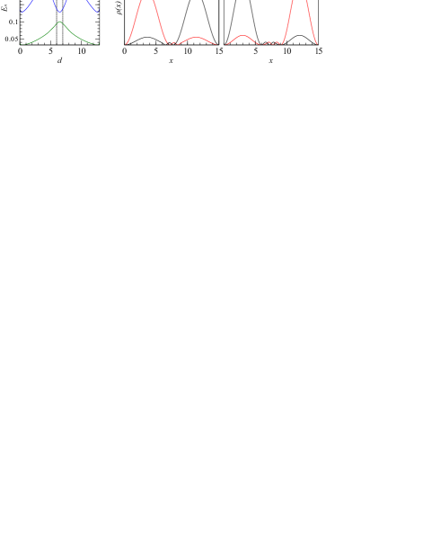
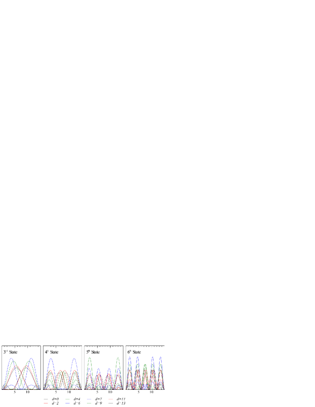
The localization of the electron, as described by the density , is also affected by the deformation. In Figure 2 we show the resulted densities for the first four positive eigenenergies, 3, 4, 5, and 6, for a selection of different values. There is a clear shifting from one side of the system to the other on the most probable position of the particle as a function of the system state. For example, for the third state, the particle is localized in the right side of the well for . The localization is shifted toward the left side for . This shifting effect persists up to higher states, although the side chosen by the system depends, among other factor, on the odd/even character of the quantum number.
So far we have shown that energy levels’ oscillations (for energies above zero) are directly related to the system’s deformation and therefore providing a way to externally control the particular values of the energy spectrum of a system. As aforementioned in the introduction section, many similar oscillations, due to other causes, were reported and in many of them the oscillations are associated with crossing avoidance. The oscillations observed in this example are also associated with density swapping between states. In Figure 3, the energies and densities of the third and forth eigenstates are shown. In the left panel, it is clear that there is a crossing avoidance at . This is associated with a density swapping where for , the third state is localized in the left of the well while the fourth state is localized in the right. This swapping happens in the reverse order for .
II.2 A symmetric multiple quantum well between infinite walls deformed by biasing
In this subsection and the next we consider two examples that could be practically achieved with currently known materials and technologies, allowing the experimental exploration of controlled energy level oscillations and the associated localization/delocalization of the particles. In this case, we start with a symmetric double-well system confined between two infinite walls. Then, a biasing voltage is applied to deform the original system into a tilted one. The unbiased potential, represented in the sketch of Figure 4, is mathematically described by the following potential:
| (6) |
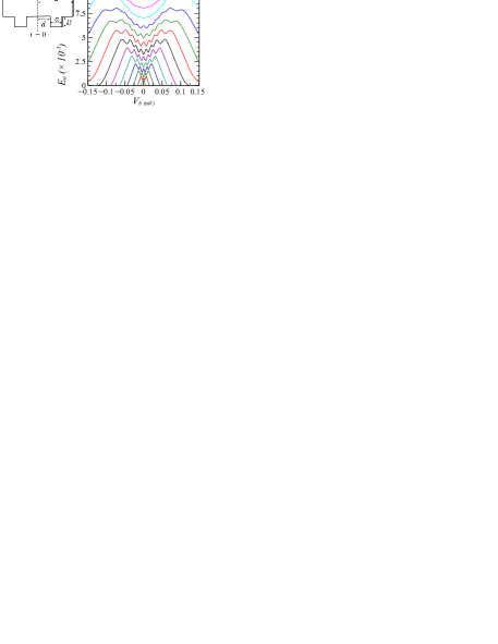
where and are positive constants and . Equivalent systems can be made although with finite potential walls. For example, using semiconductor multiple quantum wells L05 ; C04 or a double quantum dot system S11 ; H04 can be used to realize a device having the qualitative features of Eq. (6). Having this examples in mind, the parameters used in this analysis are within the ranges of practical values. We chose , and that represent 10 nm, 2 nm and 0.54 eV, respectively. By applying a biasing voltage , the potential is tilted by an additional term of providing the externally controlled deformation. In our example, the voltage is varied between -0.15 and 0.15 mV. The resulting energies are shown in Figure 4 as a function of , where it can be seen the emergence of an oscillating pattern having similar characteristics to the example of the previous section. For example, the amplitude of the oscillation is a function of the energy level, as it was found by the PT analysis presented above.
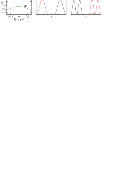
Analogously to the case of Subsection A, in this example the energy oscillation has an associated crossing avoidance and localization transition. In Figure 5 we show the energies and densities corresponding to the 11th and 12th eigenstates. In the left panel, it is clear that there is a crossing avoidance around mV. The concurrent density swapping happens upon a very small change in the biasing: for mV, the 11th state is localized in the left of the well while the 12th state is localized in the right. The picture is completely reversed for mV.
II.3 A layered 2D hybrid perovskites deformed by applying pressure
The second possible practical deformation method that we consider relies on the application of an external pressure. To realize this system we propose a layered 2D hybrid perovskites. These structures are composed of alternating layers of hybrid 2D framework of octahedra inorganic and organic cations providing the wells. Moreover, the system could be intercalated between softer polymeric layers allowing large deformations and increasing the degree of external control by the application of moderate pressure as compared with purely inorganic crystals F05 ; A03 ; S09 . These materials can be analyzed as superlattices, as shown by Even et al. E01 and the references therein.
The most studied 2D hybrid materials are \ce[RNH3]2(CH3NH3)_m-1Pb_mI_3m+1, with \ceR representing an organic group. In these materials, \cePb_mI_3m+1 forms the octahedra that include the \ce(CH3NH3) cations forming the wells. On the other hand, \ce[RNH3]2 constitutes the barriers and by changing the organic group (R), the equilibrium separation between the wells can be tailored E01 . The depth of the well is estimated to be eV T01 . As for the well width, it depends on the number of the octahedra layers. For 1, 2, 3, and 4, the thicknesses are 0.65, 1.25, 1.85, and 2.5 nm respectively T01 .
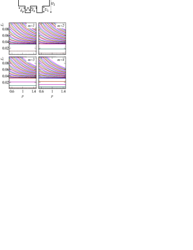
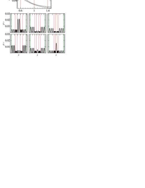
In this subsection, we study the effect of the pressure on the energy levels on the \ce[RNH3]2(CH3NH3)_m-1Pb_mI_3m+1 quantum wells with 1.25 nm barrier. A finite number of wells will be used where the whole system is then placed between two insulators with a barrier height of eV, as described in Figure 6 for the case of two wells E01 . In our approximation, the external pressure only affects the confining external layers by changing their thickness by a factor . The eigenvalues show the avoidance crossing characteristics as in the previous cases, although now as a function of the deformation parameter . This is explicitly displayed in Figure 7, in which we display two states corpsonding to the case of . As the system is deformed, the 14th energy level has the particle shifting its preferential position from the central region between the wells for , to the outermost layers for . The energy level immediately above, the situation is exactly the opposite.
III Conclusion
In this paper, we have analyzed the interplay between the detailed dimensions of a confining potential, energy level oscillations and particle’s localization. It was shown that the obtained oscillations are associated with level avoided crossings and that the deformation induces a change in the preferential spatial localization of the electrons. This effect is quite general, as shown by the the three described examples, and therefore it can be realized in different ways. The external controlling parameter could be an applied voltage or pressure, and other procedures are certainly possible. Obtaining a practical way to experimentally control the electron localization would enable the manipulation of charges in quantum confined systems and provide guidelines for the design of devices. The approach that we have used to describe the is based on simple 1D problems, but the consistent presence of this effect on multiple scenarios suggests that this phenomena is general and could be realized in 3D systems at the nanometer scale.
IV References
References
- [1] JR Petta, AC Johnson, JM Taylor, EA Laird, A Yacoby, MD Lukin, CM Marcus, MP Hanson, and AC Gossard. Coherent manipulation of coupled electron spins in semiconductor quantum dots. Science, 309(5744):2180–2184, 2005.
- [2] JM Taylor, JR Petta, AC Johnson, A Yacoby, CM Marcus, and MD Lukin. Relaxation, dephasing, and quantum control of electron spins in double quantum dots. Physical Review B, 76(3):035315, 2007.
- [3] RJ Schoelkopf and SM Girvin. Wiring up quantum systems. Nature, 451(7179):664–669, 2008.
- [4] D Vion, A Aassime, A Cottet, Pl Joyez, H Pothier, C Urbina, D Esteve, and Michel H Devoret. Manipulating the quantum state of an electrical circuit. Science, 296(5569):886–889, 2002.
- [5] O Astafiev, Alexandre M Zagoskin, AA Abdumalikov, Yu A Pashkin, T Yamamoto, K Inomata, Y Nakamura, and JS Tsai. Resonance fluorescence of a single artificial atom. Science, 327(5967):840–843, 2010.
- [6] David M Berns, Mark S Rudner, Sergio O Valenzuela, Karl K Berggren, William D Oliver, Leonid S Levitov, and Terry P Orlando. Amplitude spectroscopy of a solid-state artificial atom. Nature, 455(7209):51–57, 2008.
- [7] Thomas Niemczyk, F Deppe, H Huebl, EP Menzel, F Hocke, MJ Schwarz, JJ Garcia-Ripoll, D Zueco, T Hümmer, E Solano, et al. Circuit quantum electrodynamics in the ultrastrong-coupling regime. Nature Physics, 6(10):772–776, 2010.
- [8] M Zecherle, C Ruppert, EC Clark, G Abstreiter, JJ Finley, and M Betz. Ultrafast few-fermion optoelectronics in a single self-assembled in ga as/gaas quantum dot. Physical Review B, 82(12):125314, 2010.
- [9] Jacky Even, Laurent Pedesseau, and Claudine Katan. Understanding quantum confinement of charge carriers in layered 2d hybrid perovskites. ChemPhysChem, 15(17):3733–3741, 2014.
- [10] Gaëtan Lanty, Khaoula Jemli, Yi Wei, Joël Leymarie, Jacky Even, Jean-Sébastien Lauret, and Emmanuelle Deleporte. Room-temperature optical tunability and inhomogeneous broadening in 2d-layered organic–inorganic perovskite pseudobinary alloys. The Journal of Physical Chemistry Letters, 5(22):3958–3963, 2014.
- [11] Pablo Serra, Marcelo A. Carignano, Fahhad H. Alharbi, and Sabre Kais. Quantum confinement and negative heat capacity. Europhysics Letters, 104(1):16004, 2013.
- [12] William D Oliver, Yang Yu, Janice C Lee, Karl K Berggren, Leonid S Levitov, and Terry P Orlando. Mach-zehnder interferometry in a strongly driven superconducting qubit. Science, 310(5754):1653–1657, 2005.
- [13] Mika Sillanpää, Teijo Lehtinen, Antti Paila, Yuriy Makhlin, and Pertti Hakonen. Continuous-time monitoring of landau-zener interference in a cooper-pair box. Physical review letters, 96(18):187002, 2006.
- [14] Ronald Hanson and David D Awschalom. Coherent manipulation of single spins in semiconductors. Nature, 453(7198):1043–1049, 2008.
- [15] Lieven MK Vandersypen and Isaac L Chuang. Nmr techniques for quantum control and computation. Reviews of modern physics, 76(4):1037, 2005.
- [16] Ben Criger, Gina Passante, Daniel Park, and Raymond Laflamme. Recent advances in nuclear magnetic resonance quantum information processing. Philosophical Transactions of the Royal Society A: Mathematical, Physical and Engineering Sciences, 370(1976):4620–4635, 2012.
- [17] Sangchul Oh, Zhen Huang, Uri Peskin, and Sabre Kais. Entanglement, berry phases, and level crossings for the atomic breit-rabi hamiltonian. Physical Review A, 78(6):062106, 2008.
- [18] Sonia G Schirmer, Ivan CH Pullen, and Allan I Solomon. Controllability of multi-partite quantum systems and selective excitation of quantum dots. Journal of Optics B: Quantum and Semiclassical Optics, 7(10):S293, 2005.
- [19] Alejandro Ferrón, Pablo Serra, and Omar Osenda. Quantum control of a model qubit based on a multi-layered quantum dot. Journal of Applied Physics, 113:134304, 2013.
- [20] David D Awschalom, Lee C Bassett, Andrew S Dzurak, Evelyn L Hu, and Jason R Petta. Quantum spintronics: Engineering and manipulating atom-like spins in semiconductors. Science, 339(6124):1174–1179, 2013.
- [21] SN Shevchenko, Sahel Ashhab, and Franco Nori. Landau–zener–stückelberg interferometry. Physics Reports, 492(1):1–30, 2010.
- [22] Norman Y Yao, Liang Jiang, Alexey V Gorshkov, Peter C Maurer, Geza Giedke, J Ignacio Cirac, and Mikhail D Lukin. Scalable architecture for a room temperature solid-state quantum information processor. Nature Communications, 3:800, 2012.
- [23] Jingfu Zhang, Man-Hong Yung, Raymond Laflamme, Alán Aspuru-Guzik, and Jonathan Baugh. Digital quantum simulation of the statistical mechanics of a frustrated magnet. Nature Communications, 3:880, 2012.
- [24] Yu-Jing Zhao, Xi-Ming Fang, Fang Zhou, and Ke-Hui Song. Scheme for realizing quantum-information storage and retrieval from quantum memory based on nitrogen-vacancy centers. Physical Review A, 86(5):052325, 2012.
- [25] SN Shevchenko, S Ashhab, and Franco Nori. Inverse landau-zener-stückelberg problem for qubit-resonator systems. Physical Review B, 85(9):094502, 2012.
- [26] J-N Zhang, C-P Sun, S Yi, and Franco Nori. Spatial landau-zener-stückelberg interference in spinor bose-einstein condensates. Physical Review A, 83(3):033614, 2011.
- [27] Weidong Sheng and Jean-Pierre Leburton. Anomalous quantum-confined stark effects in stacked inas/gaas self-assembled quantum dots. Physical review letters, 88(16):167401, 2002.
- [28] Mark S Sherwin, Atac Imamoglu, and Thomas Montroy. Quantum computation with quantum dots and terahertz cavity quantum electrodynamics. Physical Review A, 60(5):3508, 1999.
- [29] T Chwiej and B Szafran. Few-electron artificial molecules formed by laterally coupled quantum rings. Physical Review B, 78(24):245306, 2008.
- [30] LC Lenchyshyn, HC Liu, M Buchanan, and ZR Wasilewski. Voltage-tuning in multi-color quantum well infrared photodetector stacks. Journal of applied physics, 79(10):8091–8097, 1996.
- [31] Alexander Högele, Stefan Seidl, Martin Kroner, Khaled Karrai, Richard J Warburton, Brian D Gerardot, and Pierre M Petroff. Voltage-controlled optics of a quantum dot. Physical review letters, 93(21):217401, 2004.
- [32] W Bardyszewski and SP Łepkowski. Pressure-dependent reordering of valence band states in gan/al x ga 1- x n quantum wells. Physical Review B, 85(3):035318, 2012.
- [33] David B Mitzi, Konstantinos Chondroudis, and Cherie R Kagan. Organic-inorganic electronics. IBM journal of research and development, 45(1):29–45, 2001.
- [34] Siegfried Flügge. Practical quantum mechanics. Springer Verlag, 1994.
- [35] Pablo Serra and Sabre Kais. Ground-state stability and criticality of two-electron atoms with screened coulomb potentials using the b-splines basis set. Journal of Physics B: Atomic, Molecular and Optical Physics, 45(23):235003, 2012.
- [36] Paul Harrison. Quantum Wells, Wires and Dots: Theoretical and Computational Physics. John Wiley & Sons, Chichester, 1st edition, 2000.
- [37] Fahhad Alharbi. An explicit fdm calculation of nonparabolicity effects in energy states of quantum wells. Optical and quantum electronics, 40(8):551–559, 2008.
- [38] Kenji Nakamura, Akira Shimizu, Masanori Koshiba, and Kazuya Hayata. Finite-element analysis of quantum wells of arbitrary semiconductors with arbitrary potential profiles. Quantum Electronics, IEEE Journal of, 25(5):889–895, 1989.
- [39] Khai Q Le. Finite element analysis of quantum states in layered quantum semiconductor structures with band nonparabolicity effect. Microwave and Optical Technology Letters, 51(1):1–5, 2009.
- [40] Fahhad Alharbi. Meshfree eigenstate calculation of arbitrary quantum well structures. Physics Letters A, 374(25):2501–2505, 2010.
- [41] Wenbin Lin, Narayan Kovvali, and Lawrence Carin. Pseudospectral method based on prolate spheroidal wave functions for semiconductor nanodevice simulation. Computer physics communications, 175(2):78–85, 2006.
- [42] R Meyer, M Dahl, G Schaack, A Waag, and R Boehler. Low-temperature magneto-optical studies of a cdte/cd 1- x mn x te quantum-well structure at high hydrostatic pressures. Solid state communications, 96(5):271–278, 1995.
- [43] Matthew P Lumb, Michael K Yakes, María González, Igor Vurgaftman, Christopher G Bailey, Raymond Hoheisel, and Robert J Walters. Double quantum-well tunnel junctions with high peak tunnel currents and low absorption for inp multi-junction solar cells. Applied Physics Letters, 100(21):213907, 2012.
- [44] Gabriel Christmann, Alexis Askitopoulos, George Deligeorgis, Zacharias Hatzopoulos, Simeon I Tsintzos, Pavlos G Savvidis, and Jeremy J Baumberg. Oriented polaritons in strongly-coupled asymmetric double quantum well microcavities. Applied Physics Letters, 98(8):081111, 2011.
- [45] Charles A Stafford and Ned S Wingreen. Resonant photon-assisted tunneling through a double quantum dot: An electron pump from spatial rabi oscillations. Physical review letters, 76(11):1916, 1996.
- [46] Xuedong Hu and S Das Sarma. Hilbert-space structure of a solid-state quantum computer: Two-electron states of a double-quantum-dot artificial molecule. Physical Review A, 61(6):062301, 2000.
- [47] Jarvist M Frost, Keith T Butler, Federico Brivio, Christopher H Hendon, Mark van Schilfgaarde, and Aron Walsh. Atomistic origins of high-performance in hybrid halide perovskite solar cells. Nano Letters, 14(5):2584–2590, 2014.
- [48] RJ Angel, J Zhao, and NL Ross. General rules for predicting phase transitions in perovskites due to octahedral tilting. Physical review letters, 95(2):025503, 2005.
- [49] Raymond E Schaak and Thomas E Mallouk. Perovskites by design: a toolbox of solid-state reactions. Chemistry of Materials, 14(4):1455–1471, 2002.
- [50] Kenichiro Tanaka and Takashi Kondo. Bandgap and exciton binding energies in lead-iodide-based natural quantum-well crystals. Science and Technology of Advanced Materials, 4(6):599–604, 2003.