Poole-Frenkel effect and Variable-Range Hopping conduction in metal / YBCO resistive switching devices
Abstract
Current-voltage (IV) characteristics and the temperature dependence of the contact resistance [] of Au / YBa2Cu3O7-δ (optimally doped YBCO) interfaces have been studied at different resistance states. These states were produced by resistive switching after accumulating cyclic electrical pulses of increasing number and voltage amplitude. The IV characteristics and the dependence of the different states are consistent with a Poole-Frenkel (P-F) emission mechanism with trapping-energy levels in the 0.06-0.11 eV range. remains constant up to a number-of-pulses-dependent critical voltage and increases linearly with further increasing the voltage amplitude of the pulses. The observation of a P-F mechanism reveals the existence of an oxygen-depleted layer of YBCO near the interface. A simple electrical transport scenario is discussed, where the degree of disorder, the trap energy level and the temperature range determine an electrical conduction dominated by non-linear effects, either in a P-F emission or in a variable-range hopping regime.
pacs:
73.40.-c, 73.40.Ns, 74.72.-hI INTRODUCTION
There is a technological need to develop faster, smaller, cheaper and more reliable memory devices, which is therefore promoting the search to improve their capacity to retain a higher density of information, at lower costs, using less energy and operating under hostile environment conditions. Burr08 ; Yang13 As possible candidates to fulfil such an overwhelming task, we can find memories (RRAM) based on the resistive switching (RS) mechanism, where the non-volatile and reversible resistance state of a metal-oxide interface is varied upon the application of electric pulses. Sawa08 In the past few years some remarkable improvements have been made to understand the physics behind the memory properties of RRAM devices. Waser07 As an example, the underlying memory mechanism of devices based on metal-perovskite oxide junctions was associated with the resistance change due to oxygen-vacancy electromigration near the interface. Rozenberg10 Despite these advances, many aspects are still unclear and should be addressed in order to improve their practical capabilities. In that sense, one important feature to determine in each particular device is the conduction mechanism that dominates its electrical transport properties. This knowledge can be the key to control most of the desired properties of a memory device as it points out which are the relevant microscopic factors that determine their resistive state. Depending on material characteristics of the metal-oxide interface, the mechanism can be electrode-limited or bulk-limited. Sze06 ; Chiu14 In the electrode-limited ones, the work function of the metal, the carrier affinity and the thickness of the oxide determine the barrier height and the probability to produce an electric-field-induced-current through the junction. In this case, the mechanism can be described as Schottky, Fowler-Nordheim or direct tunneling emission. In the bulk-limited case, the conduction mechanism is determined by the electrical properties of the oxide near the interface, particularly by the existence of traps and their energy levels. Poole-Frenkel emission (P-F) and space-charge-limited conduction (SCLC) are two examples of transport mechanisms influenced by the energy distribution and density of traps.
Metal-YBa2Cu3O7-δ (YBCO) interfaces on ceramic and thin-films samples have both shown bipolar RS characteristics. Acha09a ; Acha09b ; Placenik10 ; Acha11 Their retentivity Schulman11 ; Placenik12 as well as their response to cyclic electric field stresses Schulman12 have been previously studied. Although the microscopic origin of its RS properties was successfully associated to the electromigration of oxygen vacancies Rozenberg10 , no detailed studies of the conduction mechanism through the interface have been already performed.
In this paper, our goal is to identify the relevant transport mechanism of Au / YBa2Cu3O7-δ (YBCO) interfaces, in order to point out the microscopic factors that determine the resistive state, as the temperature dependence and magnitude of the resistance change upon producing a RS. Our results indicate that a P-F emission mechanism dominates the current-voltage dependence of the junction, consequently indicating the existence of carrier traps and of a low conductivity region in the interfacial YBCO. Within this scenario, most probably related to a random distribution of oxygen vacancies near the junction, we present a description of the electrical conduction based on a modified Variable-Range Hopping (VRH) mechanism. The modification that we propose is based on considering that the available electrical carriers are only those thermally or voltage assisted de-trapped which obey to a P-F law. In this framework, we show that increasing the amplitude or the number of applied pulses has qualitatively the same microscopic effect on modifying the trap energy level as well as the resistivity and the geometric factor of a conducting channel.
II EXPERIMENTAL DETAILS
The device was prepared by sputtering four metallic electrodes on top of a face of a good quality and optimally-doped YBCO textured ceramic slab (840.5 mm3, see the inset of Fig. 1). The YBCO slab was synthesized following a similar procedure to the one described in Ref. Porcar97 The homogeneity and the oxygen content was checked by measuring its resistive superconducting transition, which showed a 10-90% width of 2 K and a (90 0.2) K (see ref. Acha09a ). By considering the relation between and the mean oxygen content (7-)Takagi87 ; Cava90 , we estimated that 0.05. The sputtered electrodes have a 1x1 mm2 area and a mean separation of 0.5 mm. Copper leads were carefully fixed by using silver paint, without contacting directly the surface of the sample. Au and Pt were chosen as metals for the pair of pulsed electrodes, labeled and , respectively. As we have previously shown Schulman13 , the Pt / YBCO interfaces have a lower resistance value than the Au / YBCO ones (), and a small RS amplitude. Thus, we may disregard the influence of the Pt / YBCO electrode and proceed as if only the Au / YBCO electrode were active (i.e. presents a relevant RS effect), simplifying the effects produced upon voltage pulsing treatments.
In order to analyze the sensitivity of the microscopic parameters that control the electrical transport properties of the Au / YBCO interface to the voltage amplitude and to the number of applied pulses, we applied the following pulsing protocol (see Fig. 1):
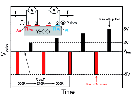
Temperature is initially stabilized at 300 K, with the active Au / YBCO electrode set to its low resistance state (). A Pt thermometer is used to determine the temperature of the device. To produce a RS to a high resistance state (), a ”reset” burst of positive unipolar pulses (500 s width at 1 kHz rate) of a amplitude () is applied with an Agilent 33250A waveform generator to electrodes 1-2, during a time (from 10 s to 500 s, depending on the value). We want to note here that the polarity of the pulses was defined arbitrarily with the ground terminal connected to the active Au / YBCO contact. With this definition, for example, a negative pulse produces a positive voltage drop on the Au / YBCO interface. In order to avoid overheating effects on the resistance measurements, a time equal to is waited before measuring the temperature dependence of remnant resistance . Then this resistance is measured as a function of temperature, cooling down to 240 K and heating back to 300 K at a 2 K per minute rate. For that, a DC three terminal method is used, by applying a small bias current (100 A) to electrodes 1-2 and by measuring the voltage difference ( 0.1 V) between electrodes 1-3. A Keithley 224 was used as current source and an Agilent 34420A as nanovoltmeter. Voltage was also measured between electrodes 2-4 to check the small RS effect of the Pt / YBCO electrode.
Also using this configuration, DC current-voltage characteristics (IV) were measured at 300 K, where a small I-V range was explored in order to avoid a RS of the active electrode. Corrections to by considering the resistance of the bulk YBCO (beyond the interfacial zone) are negligible taking into account that its value is only in this temperature range.
After the measurement, due to the bipolar nature of the RS in the metal/perovskite interface, a ”set” burst of maximum opposite polarity (-) of the same number of pulses of the ”reset” burst is applied to come back to a LRS and to erase the cumulative effects of the reset pulses. Then, the temperature dependence of the LRS remnant resistance is measured [] following the same procedure as with . The process is then completely repeated for a new value, increased with a fixed step, until it reaches our experimental maximum (). The whole process was performed for different numbers of pulses in the range.
III RESULTS AND DISCUSSION
In Fig. 2 a) the hysteretical remnant resistance of both Au / YBCO and Pt / YBCO contacts ( and , respectively) after applying a burst of 100 pulses of amplitude can be observed. As is varied following a loop, these curves are usually called Resistance Hysteresis Switching Loop (RHSL). The observed bipolar memory behavior of both contacts and their complementary response to is a typical characteristic of the RRAM devices. Acha09b ; Rozenberg10 ; Acha11 It can be noticed the lower switching amplitude and the better stability of in comparison to , in accordance to the expected passivity of the former. Taking this into account, hereafter our results and discussions will be only related to the Au / YBCO active electrode.
In Fig. 2 b), the relative amplitude of the remnant resistance change at room temperature, defined as , is presented as function of and for different numbers of applied pulses (). As shown in a previous study Schulman13 , increases logarithmically with increasing and follows a power-law-like dependence with (if is higher than a -dependent threshold voltage, ). A similar result has been observed for Ag / manganite interfaces and was interpreted as a consequence of the voltage and history dependent spatial distribution of oxygen-vacancies near the interface. Ghenzi12
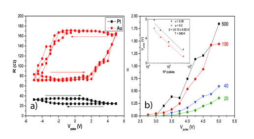
The inset of Fig. 2 shows the -N curves that produce different values (0.2 and 0.35) which recalls a similar behavior to that described by the Basquin law of mechanical stress-lifetime test, which corresponds to Schutz96 ; Suresh98 , with -0.1.
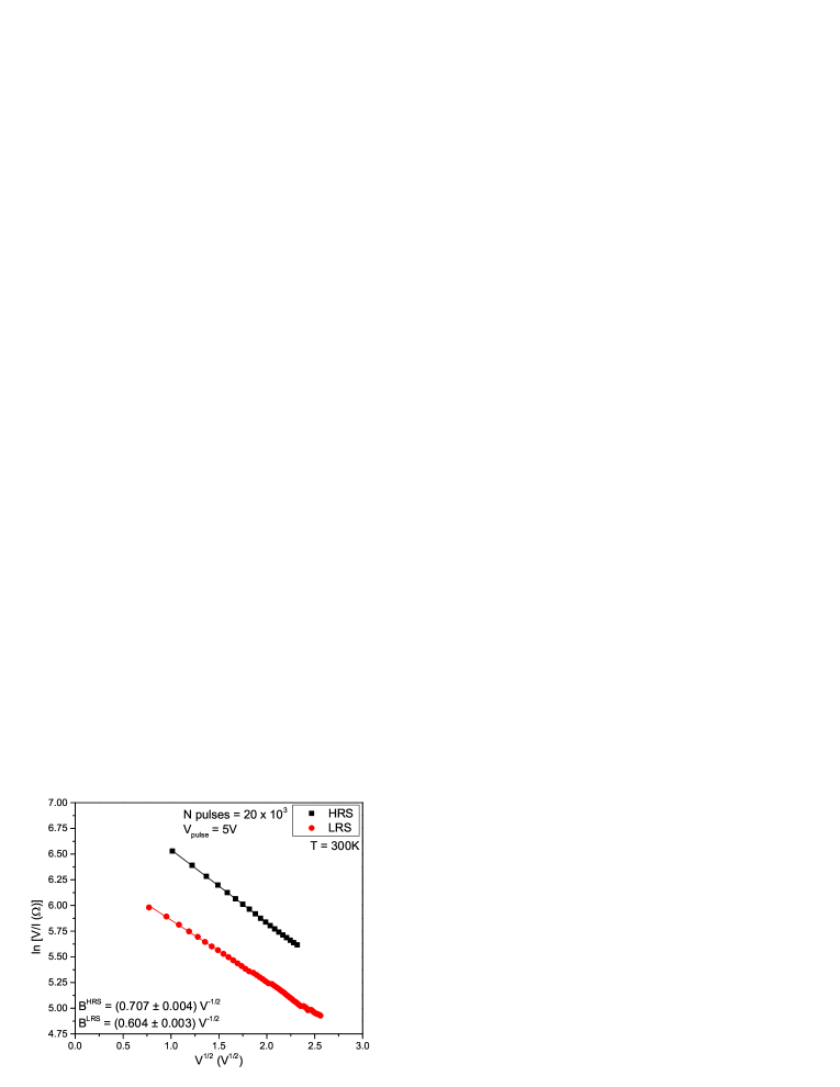
From the IV characteristics obtained for both states at 300 K, we have plotted a typical result as vs in Fig. 3. Data is well fitted by a linear dependence although there are some small deviations at low voltages. This result indicates that bulk-limited P-F emission is the dominant mechanism for the electrical transport of carriers through this interface. This can be seen by considering the expression of the P-F current () as a function of the voltage at a fixed temperature , which corresponds to Simmons67
| (1) |
with
| (2) |
where is a pre-factor that will be discussed later, associated with the geometric factor of the conducting path, the electronic drift mobility () and the density of states in the conduction band. is the trap energy level, the Boltzmann constant, the electron charge, the dielectric constant of the oxide and the distance between electrodes. The voltage-dependent contact resistance can then be expressed as:
| (3) |
From the values obtained by fitting the data presented in Fig. 3 with Eq. 3 and by assuming that the dielectric constant of YBCO Mannhart96 is of the order of 200 F/m, the characteristic distance , where most of the voltage drops occurs, can be estimated. We obtain that 0.8 m and 1.1 m, which corresponds to a size much lower that the distance between contacts ( 500 m), in accordance to previous results that indicate that the RS-active-region remains limited to a small zone near the interface. Wang12
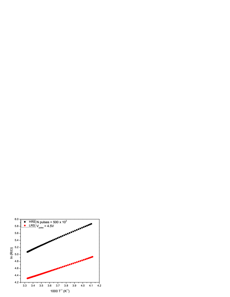
As the measurements were performed using low currents, the remnant non-linear (NL) contact resistance (Eq. 3) should be nearly ohmic when , where . In that case, Eq. 3 can be simplified as
| (4) |
Fig. 4 shows the temperature dependence of the Au / YBCO contact resistance in both states (LRS and HRS) plotted as ln(R)vs in the 240 K to 300 K temperature range. The sensitivity of can be observed in Fig. 5, where ln(R)vs is shown for varying and a fixed . Similar results were obtained for the whole set of values explored (not shown here). The nearly straight line followed by the data in this temperature range indicates a good agreement with Eq. 4, implying that and should be practically temperature-independent. and for pulses can then be extracted for both states (LRS and HRS) by using Eq. 4 to fit the data presented in Fig. 4 and Fig. 5. A similar procedure was followed for other values of .

The fitting values are shown in Fig. 6 for the whole set of pulses per burst explored. The obtained values for both states and for all pulsing treatments are within the 0.06 eV to 0.11 eV range, which validates the approximation made to obtain Eq. 4 ( 10 V). It can be observed that in the low voltage region [], is nearly voltage independent, but decreases with increasing as a consequence of the decrease of , due to the set pulsing treatment (see Fig. 1). For , increases linearly with with a slope of 0.025 eV V-1 and becomes less -dependent. This voltage dependence with a relatively low N-dependence is in accordance to the previously observed behavior Schulman13 , mentioned as a Basquin-like law. This law indicates that the amplitude of the RS change () is more sensible to a voltage variation than to a number of pulses change. In this way, to produce the same RS effect, should be increased by 3 orders of magnitude if is reduced to half its value.
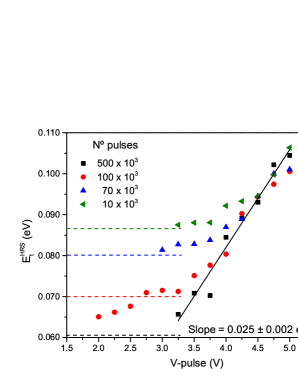
The obtained dependence for different bursts
lengths is shown in Fig. 7. Besides the noisy
behavior, two regions can be observed as for : a voltage
independent region for and, surprisingly, a
tendency to decrease for .

On one hand, as our results indicate that the main conduction mechanism through the Au/YBCO interface is a P-F emission, we have to consider that transport properties are dominated by a carrier-trap region in the YBCO part of the junction. In that sense, YBCO in this interface-active-region cannot be in a metallic-like state, even at room temperature or in the LRS, which indicates that the average density of oxygen-vacancies () should be roughly in the 0.7 to 1.0 range. Wuyts96 For these values, YBCO is not superconducting and has resistivities in a broad range, from 4 to 4000 mcm. Matsushita87 ; Milliken00 Oxygen vacancy zones can then be considered as the positively-charged traps that will capture electrons, impeding hole mobility. They are, up to now, associated with the microscopic origin of the bipolar RS effect and models based on their electromigration manage to describe nontrivial experimental results. Rozenberg10 Here, the fact that increases with increasing may indicate that oxygens are not removed uniformly from the YBCO lattice, but in a correlated manner, increasing the size of oxygen-depleted spots, probably as the local electric field is larger in these zones. As it will be discussed later, the decrease of with can be related to an increase of the cross-section area of a low-conducting filament in the HRS.
On the other hand, it was shown Matsushita87 ; Milliken00 that the electrical conduction of low-oxygen-content YBCO is by a 2D variable range hopping (2D-VRH) mechanism, as oxygen vacancies introduce disorder in the electronic potential. Efros84 At the same time, we may consider the scenario here depicted, where part or the totality of the hopping carriers can be trapped in deeper potential wells, associated with the electric-pulse-induced oxygen vacancy spots. In this case, their number will be limited, introducing a characteristic de-trapping energy () and the NL characteristics of the P-F effect.
The standard 2D-VRH resistivity () of the oxygen-depleted YBCO near the interface can be expressed as:
| (5) |
where is a parameter related to the localization length and to the density of states at the Fermi energy, and
| (6) |
where is the density of carriers, the electron’s charge, a characteristic phonon-assisted hopping frequency and the hopping distance.
This expression should be modified to consider the influence of traps. If the density of traps and if we assume that at T=0 K all the electrical carriers are trapped, only those de-trapped or ionized () will participate in the VRH conduction. As the barrier to overcome () can be reduced by the P-F effect, then . Within this scenario, the contact resistance associated with an oxygen-depleted YBCO zone of characteristic length and a conducting area can be rewritten as:
| (7) |
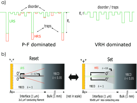
In fact, as the disorder that produces the VRH conduction can be associated with an oxygen-vacancy random distribution, which may produce trapping centers for the carriers that yield to a P-F emission, both conduction mechanisms may coexist or dominate, depending on different factors: as stated in Eq. 7, VRH should be the main mechanism for temperatures with . While for the conduction should be of the P-F type. In the same way, NL effects should be observed for voltages in the P-F case, and may even be detected when . While in the VRH regime, they should be noticed for a low temperature region, where . On other words, depending on the degree of disorder, on the trap energy level and on the temperature range explored, low-oxygen-content YBCO can present, intrinsically, a VRH or a P-F regime, as well as NL-IV characteristics. The VRH the NL-IV regime was in fact observed previously Matsushita87 for YBa2Cu3O6, where the electrical transport properties, measured in a four terminal configuration at 40 K to 300 K, were well described by a 2D-VRH conduction and showed the presence of a NL regime at low temperatures, whose origin has not been discussed so far. Conversely, our results in the Au / YBCO junctions for the 240 K to 300 K temperature span indicate that the P-F emission is favored over the VRH regime. In that way, the interfacial region of YBCO may present higher trap energy levels (oxygen-depleted spots) and a less disordered crystal structure than that existing in the oxygen-depleted YBCO with . As mentioned, this can be related to a correlated oxygen vacancy distribution, which increases the trap energy level without increasing the overall disorder, as in a random vacancy distribution. A sketch of these possible two scenarios is presented in Fig. 8a).
The mentioned low conductivity of the pristine YBCO in contact with the Au interface may be a consequence of the higher oxidation energy of Au when compared to YBCO. One possibility (see Fig. 8b) is that Au depleted oxygens from the interfacial YBCO, generating a disordered potential with traps for the charge carriers.
Just to give an order of magnitude, we can assume that this interfacial YBCO has a mean density of vacancies of 0.7 to 1 per unit cell volume ( 61021 cm-3) in the LRS and in the HRS, respectively. In this case, should range from 4 mcm to 4000 mcm. Wuyts96 ; Matsushita87 In these conditions, the conduction area can be roughly estimated by considering Eq. 7 and the low voltage measurements of the contact resistance at 300 K. The obtained values, 22 m2 and 9090 m2, indicate the filamentary nature of the area modified by the RS pulsing treatments. The dispersive diffusion of oxygens may be the reason of the increase of when compared to . Although for YBCO increases with increasing , the increase of determines the decrease of with (see Fig. 7). Local measurements of the oxygen content near the interface are needed to prove the validity of this sketched scenario.
IV CONCLUSIONS
In summary, transport measurements performed on Au / optimally-doped YBCO as a function of temperature and electric field showed an electrical conduction dominated by a P-F emission mechanism. As this is a bulk property of the interfacial YBCO, we inferred that in a 1 m region near the interface, YBCO is oxygen-depleted, in a way that favors the existence of traps for the carriers. The energy level of these traps () can be increased linearly by increasing the amplitude of the voltage pulses. This result can be interpreted as an indication that the electromigration of oxygens may not be produced randomly but in a correlated manner. The number of applied pulses produces less changes on than those obtained by increasing , in accordance to a previously stated similarity with the stress-lifetime Basquin law. We also proposed a simple description of the intrinsic transport scenario for oxygen-depleted YBCO, where the VRH carriers may be trapped by oxygen vacancies, yielding to P-F emission or to VRH conduction, with or without NL effects, depending on the temperature range explored. Finally, an estimation of the conduction area for both states reveals the filamentary nature of the zone influenced by the pulsing treatments.
V ACKNOWLEDGEMENTS
We would like to acknowledge financial support by CONICET Grant PIP 112-200801-00930, PICT 2013-0788 and UBACyT 20020130100036BA (2014-2017). We also acknowledge V. Bekeris and F. Acha for a critical reading, and D. Giménez, E. Pérez Wodtke and D. Rodríguez Melgarejo for their technical assistance.
References
- [1] G. W. Burr, B. N. Kurdi, J. C. Scott, C. H. Lam, K. Gopalakrishnan, and R. S. Shenoy. IBM J. Res. & Dev., 52:449, 2008.
- [2] J. J. Yang, D. B. Strukov, and D. R. Stewart. Nature Nanotechnology, 8:13, 2013.
- [3] A. Sawa. Materials Today, 11:28, 2008.
- [4] R. Waser and M. Aono. Nature Materials, 6:833, 2007.
- [5] M. J. Rozenberg, M. J. Sánchez, R. Weht, C. Acha, F. Gomez-Marlasca, and P. Levy. Phys. Rev. B, 81:115101, 2010.
- [6] S. M. Sze and K. K. Ng. Physics of Semiconductor Devices. John Wiley & Sons, 2006.
- [7] F-Ch Chiu. Advances in Materials Science and Engineering, 2014:578168, 2014.
- [8] C. Acha and M. J. Rozenberg. J. Phys.: Condens. Matter, 21:045702, 2009.
- [9] C. Acha. Physica B, 404:2746, 2009.
- [10] A. Plecenik, M. Tomasek, T. Plecenik, M. Truchly, J. Noskovic, M. Zahoran, T. Rocha, M. Belogolovskii, M. Spankova, S. Chromik, and P. Kus. Appl. Surface Science, 256:5684, 2010.
- [11] C. Acha. J.Phys.D: Appl.Phys., 44:345301, 2011.
- [12] A. Schulman and C. Acha. MRS Proceedings, 1337:q10–07, 2011.
- [13] T. Plecenik, M. Tomasek, M. Belogolovskii, M. Truchl, M. Gregor, J. Noskovic, M. Zahoran, T. Roch, I. Boylo, M. Spankova, S. Chromik, P. Kus, and A. Plecenik. J. Appl. Phys., 111:056106, 2012.
- [14] A. Schulman, M. J. Rozenberg, and C. Acha. Phys. Rev. B, 86:104426, 2012.
- [15] L. Porcar, D. Bourgault, J. M. Barbut, M. Barrault, P. Germi, and R. Tournier,. Physica C, 275:293, 1997.
- [16] H. Takagi, S. Uchida, H. Iwabuchi, H. Eisaki, K. Kishio, K. Kitazawa, K. Fueki, and S. Tanaka. Physica B+C, 148:349, 1987.
- [17] R.J. Cava, A.W. Hewat, E.A. Hewat, B. Batlogg, M. Marezio, K.M. Rabe, J.J. Krajewski, W.F. Peck Jr., and L.W. Rupp Jr. Physica C: Superconductivity, 165:419, 1990.
- [18] A. Schulman and C. Acha. J. Appl. Phys., 114:243706, 2013.
- [19] N. Ghenzi, M. J. Sánchez, M. J. Rozenberg, P. Stoliar, F. G. Marlasca, D. Rubi, and P. Levy. J. Appl. Phys., 111:084512, 2012.
- [20] W. Schutz. Engineering Fracture Mechanics, 54:263, 1996.
- [21] S. Suresh. Fatigue of Materials. Cambridge University Press, 1998.
- [22] J. G. Simmons. Phys. Rev., 155:657, 1967.
- [23] J Mannhart. Superconductor Science and Technology, 9:49, 1996.
- [24] Zhi-Hong Wang, Yang Yang, Lin Gu, H-U Habermeier, Ri-Cheng Yu, Tong-Yun Zhao, Ji-Rong Sun, and Bao-Gen Shen. Nanotechnology, 23:265202, 2012.
- [25] B. Wuyts, V. V. Moshchalkov, and Y. Bruynseraede. Phys. Rev. B, 53:9418, 1996.
- [26] A. Matsushita, T. Oguchi, K. Kimura, T. Matsumoto, T. Hatano, K. Ogawa, and S. Takayanagi. Jap. J. Appl. Phys., 26:L1953, 1987.
- [27] F. P. Milliken, T. Doderer, R. H. Koch, and C. C. Tsuei. Phys. Rev. B, 62:9143, 2000.
- [28] B. I. Shklovskii and A. L. Efros. Electronic properties of doped semiconductors. Springer-Verlag, 1984.
- [29] K. M. Kim and Ch. S. Hwang. Applied Physics Letters, 94:122109, 2009.