Quantum simulation of ZnO nanowire piezotronics
Abstract
We address the problem of quantum transport in a nanometre sized two-terminal ZnO device subject to an external strain. The two junctions formed between the electrodes and the ZnO are generally taken as Ohmic and Schottky type, respectively. Unlike the conventional treatment to the piezopotential, we treat it as a potential barrier which is only induced at the interfaces. By calculating the transmission coefficient of a Fermi-energized electron that flows from one end to the other, it is found that the piezopotential has the effect of modulating the voltage threshold of the current flowing. The calculations are based on the quantum scattering theory. The work is believed to pave the way for investigating the quantum piezotronics.
pacs:
03.65.Sq, 7.55.hfI Introduction
Piezotronics, coined by Zhonglin Wang in 2007 Wang (2007), refers to the fabricated electronics whose charge transport behaviour across a metal/semiconductor interface or a p-n junction can be tuned by inner-crystal piezopotential that plays the role of the gate voltage. ZnO as a piezoelectric material possessing two important properties, i.e., semiconductive and piezoelectric, has been extensively studied as one of the most ideal candidates for piezotronic devices, and many applications materialized by ZnO such as actuators, sensors and energy harvesting devices have been achieved. For example, pH, glucose and protein sensors fabricated using metal-ZnO micro/nanowire-metal (MSM) structure were realized in Pan et al. (2013) Yu et al. (2013a) Yu et al. (2013b). Instead of using a single nanowire, wearable devices and pressure mapping sensors fabricated by ZnO nanowire arrays were explored in Xue et al. (2013) Pradel et al. (2014) Bao et al. (2015) as well. Resistive switching devices were also achieved using ZnO nanowire arrays Li (2013).
The fundamental physics behind the nanogenerator based on the ZnO nanowire has previously been discussed. The Schottky theory to explain the tunability of current transport in the piezotronics is deemed as the mainstream. It was argued that the piezopotential induced at the interface of the MS is behaving as a potential modulator (gate voltage) which exists in a certain width, and the framework has been systematically presented by Zhang et al. in Zhang et al. (2011), and the theory was further developed into a new branch called piezo-phototronics by Liu et al. in Liu et al. (2014). These two studies have provided reasonable explanations for the experiments. However, the theory constructed by the above literatures is still under the consideration of classical physics, i.e., the classical current-voltage formula in the semiconductor physics for calculating the current have been employed Zhang et al. (2011). This is satisfactory for investigating the device which has a relatively larger scale Vladimir V.Mitin and Stroscio (2008) (L de Broglie wavelength of an electron) but may not be very appropriate for the scale when the quantum effect cannot be ignored (for example: L ) . In the latter case, the quantum effect will affect the working status of the device, and some unexpected quantum phenomenons emerge. Therefore, constructing the theory of the electron transport in piezotronics with the contents of quantum physics is becoming desirable. Especially nowadays, the devices are drastically decreased in size with the rapid development of fabrication techniques. The development of the theory will benefit to the exploration of the quantum piezotronics. In this work, investigation has been conducted to understand the quantum physics of the electron transport in piezotronic nano devices. By taking M-S-M ZnO structure that has ballistic length as a paradigm, we postulate the theoretical work for calculating the electrical current in the two-terminal device. We treat the electron transport from the perspective of quantum scattering theory. Instead of seeing the electron as a classical partial, the electron is treated as a quantum wave. The piezopotential induced at the interface were assumed to be taking up a certain width Zhang et al. (2011), while in this work the piezopotential is calculated only at the interface, which is believed to be more accurate, in particular, for the very short device. The work is believed to shed some light on understanding the next-generation quantum piezotronic devices. The theoretical analysis will be given in the section 2, where the basic background of the model and the fundamental view of the electron transport in the two-terminal device are described. Numerical simulation that is based on the reasonable parameters will be conducted in the section 3, and finally the conclusion is presented in the section 4.
II Theoretical Analysis
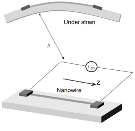
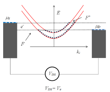
In the device (schematically shown in Fig. 1), the ZnO nanowire is seen as a quantum wire, which is very short in -direction (about 80nm) and has an extremely small area of cross section in plane. The electron transport in -direction can be seen as ballistic, and only a few electron energy states exist in plane. For an electron in quantum wire, its energy is given by:
| (1) |
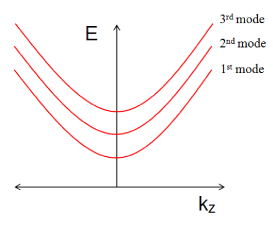
where the electron in -direction is modelled by plane waves with wave number . is the Planck’s constant divided by . and are energy quantum number in and directions, respectively. is the effective mass of the electron. and are the lengths in plane. Three modes of the energy in quantum wire are plotted in Fig. 2. The electrons in the nanowire will occupy the energy level from low to high, and in the equilibrium state the highest occupied energy is called quasi Fermi levels, represented by for electrons with and for the electrons with .
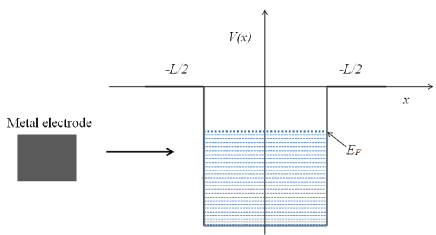
The left (Source) and right (Drain) electrodes of the device are assumed to be reservoirs of electrons, i.e., the electrons are kept presumably in equilibrium state, even under an applied voltage. The potential inside of the electrodes is approximately constant while the potential at the boundaries has a step which confines the electrons. The whole potential profile of the electrodes can be seen as a finite square well as shown in Fig. 3. The allowed kinetic energy and wave functions of electrons inside of the electrodes can be obtained straightforwardly by solving the Schrodinger equation, as:
| (2) |
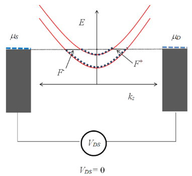
where is the length of the electrodes in -direction and (=1,2,3…) is the energy quantum number. is -direction component of wave vector at energy state . The electrons occupy the energy state according to the Pauli exclusion principle that demands one energy state can only be taken by two electrons if considering the spin. The highest energy state occupied by electrons is Fermi energy or so-called chemical potential . When the electrodes and the ZnO nanowire are connected and there is no bias applied to and , the Fermi energy must be constant through the device. Otherwise, there will be current flowing. This scenario is plotted in Fig. 4, where the chemical potential , , and are being flat. The number of electrons with wavenumber equals to the number of the electrons with wavenumber so there is not current. If a DC voltage is applied to the source () and drain (), the electron equilibrium state will be broken. As shown in Fig. 5 the unbalance between the electrons with and occurs with is higher than , which leads to some uncompensated electrons that have energy between and - flowing into the drain, i.e., current induced. The quasi Fermi level now has the following relations with chemical potential, which are: and . Also, the relation of the shift between the potential energies of electrodes and the applied is given by , where is the charge of a single electron.
Under an applied voltage , the current in a ballistic quantum wire is given by the famous Landauer formula, which is:
| (3) |
is the current brought by the uncompensated electrons. However, in this device, the quantum wire is made by ZnO, which is semiconducting material, and the electrodes are made of metals such as Ag. When a two-terminal device is fabricated, the M-S interfaces would be formed into ohmic or Schottky junction. In this work, we consider the general case, that is ohmic at left end and Schottky at right. Due to the depletion region formed at the interface, the current , therefore, transmits through the device partially, and the transmitted current can be obtained by:
| (4) |
where is the transmission coefficient for an electron that has the Fermi energy in the left electrode. From Eq. (4), it can be seen that the problem of calculating the current in the short device is transformed into a quantum scattering problem. Thus, the key is to analyse the transmission coefficient .
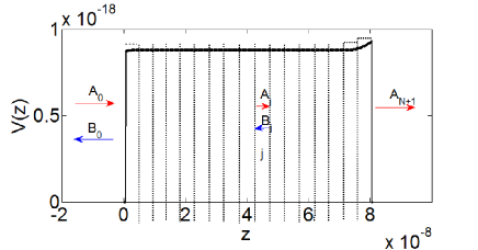
In order to calculate the , a method that can be used to calculate the transmission coefficient of arbitrary potential barrier is used Ando and Itoh (1987). As shown in the Fig. 6, the potential inside the wire in -direction has been divided into many small rectangles, the potential of segment is given by , where is the number of the segment(=0, 1, 2, 3, … N, N+1), and is the potential energy of the whole device including the electrodes. If the is taken larger and larger, the continuous potential variation will be recovered gradually. For a single rectangular potential barrier , the time-independent wavefunction of an electron inside is described by the Schrodinger equation:
| (5) |
where the is the overall energy of the electron. The wave function of can be derived easily:
| (6) |
where . According to the quantum theory, the and should be continuous at each boundary, then the amplitude and can be determined by the following equation Ando and Itoh (1987):
| (11) |
where is given by:
| (14) |
and .The scattering matrix can then be obtained as:
| (17) |
Finally, the can be calculated by: , provided the =1 and =0.
The potential energy function has to be clarified if calculating the by the above method. First, the potential variation under an applied is assumed to be linear as the quantum wire is not a perfectly metallic wires but a short nanoscale device, and the electrodes have a relatively bigger cross-section area. The source and drain capacitances can then be simply represented by parallel plate capacitors. The potential energy in the wire can be described by:
| (18) |
where is total electrostatic capacitance at point at , and and are the capacitance linking the point at to drain and source, respectively. is the initial potential energy field of the electrons in the quantum wire. We have presented the picture of potential in Fig. 6, where at the left end and right end the potential variations due to the M-S contact have been considered. The in the M-S contact region can be calculated by Poisson equation, In the simulation, when calculating the potential of the Schottky junction, we use the equation , where the origin is taken at the right interface, and the direction of is pointing to the left. As the electron flows from the left to the right, the Schottky at the right end is forwardly biased. The is the depletion layer width, and it can be obtained as . is the donor density and is the built-in potential which can be calculated easily with the work function of the electrode. Similarly, the variation potential energy in a ohmic junction can be derived by passion equation as well, i.e. , where is the width of the charged region where ohmic junction is formed. Apart from the charged region at the two interfaces, the in the rest region can be derived by continuous condition.
It should be noted that we have ignored the charging effect of the wire in Eq. 18, assuming one electron that flows into the nanowire would not affect the local potential. Substituting , into Eq. 18, the can then be explicitly expressed as:
| (19) |
When the substrate of the device is stretched or compressed, there will be strain induced in the quantum wire along the -axis, and due to the piezoelectricity, the quantum wire will generate piezoelectric charge at the interface of the ZnO wire and the electrode. Meanwhile, the induced piezoelectric charges change the local electrical field and the potential. Thus at the left and right interfaces, the piezopotential has to be considered according to piezoelectricity theory. Assuming there is a tensile stain in z-direction, then negative charge will be induced at the right interface and positive charge will be at the left interface, and if we define the density of the piezoelectric charge induced at the interface is at the two interfaces, the piezoelectric potential can be obtained by using the Poisson equation:
| (20) |
Take the left interface for instance, by integrating the Eq. 20 over the piezoelectric width , we can get:
| (21) |
Overall, under an applied voltage , and meanwhile, suffering a strain along the -axis, the potential in the device can be represented by a piece wise function, that is:
| (27) |
where and are the potential in the two electrodes, is the piezoelectric potential generated at the interface, which depends on the strain at the point . and are the assumed width that has piezoelectric charge at the left and right interface, respectively. For the left () and right () region, where the potential is constant, the solutions to the Schrodinger equation are plane waves, which are expressed as:
| (28) |
and
| (29) |
with and as the wavenumber, where is the total energy of the electron. In this work, only the electrons that come from the source are considered so the plane wave that come from drain are ignored, i.e. . Combining the Eqs. 6 - 16, the transmission coefficient () of an electron that has Fermi energy can be numerically calculated.
III Numerical Simulation and Discussion
For the ZnO nanowire, the ballistic channel length can be evaluated by comparing the transit time and its average scattering time , that is
| (30) |
where is the effective mass of the electron and is electron’s mobility. Assuming the =1 V, =500 and The is calculated, when =1, to be about 92 nm. In our simulation the length of the nanowire will be taken as 80nm as to satisfy the ballistic transport regime.
As the is very narrow (), the variation of the can be ignored, and we take equal to the width of one segment. For the right interface, the induced charge is positive so the at right interface is negative, and by symmetry we can take the to represent the piezoelectric voltage over there. As the polarization of the piezoelectric can also be expressed as: , the can then be re-written as: , in which the strain and the piezoelectric potential is related Zhang et al. (2011). The strain is varying in [-0.5/100, 0.5/100] in this simulation. The piezoelectric constants are taken as =-0.51 , =1.22 and =-0.45, respectively, and the relative dielectric constant =8.91. The material of the two electrodes is Ag. The donor density in the ZnO is taken as . The built-in potential of the Schottky barrier =0.3 eV. An electron that comes from the source with . The potential field in the nanowire is divided into 360 grids ( to ).
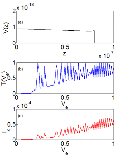
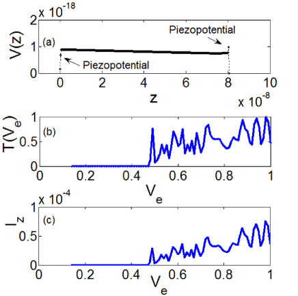
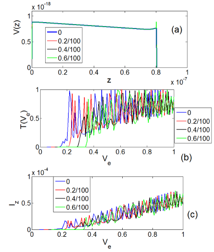
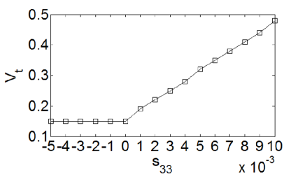
Based on the parameters taken above, the potential energy diagram of the device including two electrodes has been plotted in Fig. 6, where the Schottky barrier at the right side is about 0.3 eV, and an electron that have energy from the left electrode with amplitude and is shown, represented by the red and blue arrows in the figure. The amplitude of the incoming electron in each segment are presented by and , and when the electron reach the right electrode, it has only the amplitude as we assume there is no electron coming from right electrode. The transmission coefficient when there is no strain in the nanowire is firstly calculated in Fig. 7. In Fig. 7(a), the potential energy diagram under the applied voltage is shown. The potential is linearly decreased from the left to right, as we added the negative voltage to the left. In Fig. 7, it is seen the variation of the versus applied voltage . The transmission coefficient displays a bit nonlinearity while in some regions the is oscillating periodically due to the resonance through the virtual states above the barrier. In Fig. 7(c), the current with the varied applied voltage has been plotted by employing the quantum transport Eq. 4. Furthermore, when there is a strain of 0.5/100 along the -axis of the device, the potential diagram, transmission coefficient and quantum current have been calculated in Fig. 8. As we can see in Fig. 8, due to the strain, the piezopotential is appearing at the two interfaces, indicated by the arrows. Using this method, we can accurately model the piezopotential. In the conventional treatment, the piezopotential can only be assumed in the layer Zhang et al. (2011). In Figs. 8(b) and (c) the transmission coefficient and transmitted current versus under the strain of 0.5/100 have been plotted. Compared with Figs. 7(b) and (c), there is less oscillation, and the switch voltage for opening up the device is increased. That is because the piezopotential induced at the interface have led to the potential inside the device discontinuous as well as making the barrier at the right interface higher. Fig. 9 displays results for energy band, -, and - for various strains. The results reflect a combination of the asymmetric and symmetric effects. When the strain is 0, there is no piezoelectric effect. Combined piezoelectric and piezoresistance effects appear as the device under a non-zero strain. In order to investigate how the strain affects the switch voltage of the device, we have calculated the switch voltage when the device is suffering the external strain from -0.5/100 to 0.5/100, it is found from Fig. 10 that when the device is compressed the switch voltage keeps constant, while the threshold will be increased linearly when the device is stretched. That is because the current transport in this device is determined by the barrier at the right, and only if the device surfers a stretched strain the barrier at the right interface become higher. Under the quantum regime, the piezopotential is considered as being induced by surface charges and has no significant effect on the Schottky potential in the nanowire body. Therefore as the device under a tensile stress, the piezopotential is larger than the Schottky barrier height (SBH), rising up . On the contrary, as the piezopotential is smaller than the SBH for the case of the device having a compressive strain, the is constant (governed by the SBH).
IV Conclusion
As the device dimension reduces to the scale comparable to the de Broglie length, quantum mechanics theory has to be used. In this paper, quantum analysis of the piezotronics of ZnO two-terminal device has been performed. One dimensional chemical potential of the device has been derived including the strain induced charges and the Schottky junction effect. Transmission probability of electrons along the calculated potential has been calculated using the quantum scattering theory. It is found that the threshold point of the gate voltage has been influenced by the piezoelectric effect, which coincides with the results from the conventional theory. Moreover the electrical current fluctuates when the gate voltage is at threshold region due to quantum tunnelling resonance.
References
- Wang (2007) Z. L. Wang, Advanced Materials 19, 889 (2007).
- Pan et al. (2013) C. F. Pan, R. M. Yu, S. M. Niu, G. Zhu, and Z. L. Wang, Acs Nano 7, 1803 (2013).
- Yu et al. (2013a) R. M. Yu, C. F. Pan, J. Chen, G. Zhu, and Z. L. Wang, Advanced Functional Materials 23, 5868 (2013a).
- Yu et al. (2013b) R. M. Yu, C. F. Pan, and Z. L. Wang, Energy and Environmental Science 6, 494 (2013b).
- Xue et al. (2013) X. Y. Xue, Y. X. Nie, B. He, L. L. Xing, Y. Zhang, and Z. L. Wang, Nanotechnology 24 (2013).
- Pradel et al. (2014) K. C. Pradel, W. Z. Wu, Y. Ding, and Z. L. Wang, Nano Letters 14, 6897 (2014).
- Bao et al. (2015) R. Bao, C. Wang, L. Dong, R. Yu, K. Zhao, Z. L. Wang, and C. Pan, Advanced Functional Materials , 2884 (2015).
- Li (2013) L. Li, Applied Physics Letters 103, 233512 (2013).
- Zhang et al. (2011) Y. Zhang, Y. Liu, and Z. L. Wang, Advanced Materials 23, 3004 (2011).
- Liu et al. (2014) Y. Liu, Y. Zhang, Q. Yang, S. Niu, and Z. L. Wang, Nano Energy , doi:10.1016/j.nanoen.2014.11.051 (2014).
- Vladimir V.Mitin and Stroscio (2008) V. A. K. Vladimir V.Mitin and M. A. Stroscio, Introduction to Nanoelectronics Science, Nanotechnology, Engineering, and Applications (Cambridge University Press, 2008) pp. 167–168.
- Ando and Itoh (1987) Y. Ando and T. Itoh, Journal of Applied Physics 61, 1497 (1987).