Appearance of effective surface conductivity – an experimental and analytic study
Abstract
Surface conductance measurements on p-type doped germanium show a small but systematic change to the surface conductivity at different length scales. This effect is independent of the structure of the surface states. We interpret this phenomenon as a manifestation of conductivity changes beneath the surface. This hypothesis is confirmed by an analysis of the classical current flow equation. We derive an integral formula for calculating of the effective surface conductivity as a function of the distance from a point source. Furthermore we derive asymptotic values of the surface conductivity at small and large distances. The actual surface conductivity can only be sampled close to the current source. At large distances, the conductivity measured on the surface corresponds to the bulk value.
pacs:
73.25.+i, 72.10.Bg, 72.80.Cw, 68.35.bgI Introduction
Surface conductance measurements at micron and sub-micron scales belong to popular experimental routines characterizing semiconductor surfaces, see Ref. Hasegawa, ; Hofman1, ; Simons, . The motivation comes from microelectronics Simons as well as from molecular electronics projects, and the results depend mainly on the system under investigation. The underlying physics may be determined mostly by surface states Lublin ; Wolkow , by some bulk features or a mixture of these two limiting cases Hoffmann ; RSI . In the first case, quantum transport theory may be applied to understand the results, e.g. Ref. Lublin, . While in the latter case, classical conductance theory is effective. Surprisingly, the understanding of this well-established theory in the context of surface measurements is poor, making even a qualitative interpretation of experimental data rather difficult.
Conductance measurements on beveled surfaces have been used successfully to reconstruct the doping profile below the surface with a spreading resistance analysis spa1 ; spa2 ; spa3 . These methods, however, rely on refined numerical algorithms and offer no analytic insight. As such, they are an important tool in quantitative analysis but poorly contribute to our physical comprehension.
Recently, we have reported surface conductance measurements obtained for germanium samples with an atomically clean (001) surface APL . The results were interpreted within the classical theory without any reference to the surface states. We observed a slight but systematic change of the measured conductivity when varying the distance between current sources. Our assumption was, that this was due to the change of the conductivity beneath the surface as a result of Fermi level pinning, a phenomenon resulting in variations of charge carrier densities near the surface. Such modeling of the subsurface region was numerically explored for the surface measurements on Si(111)Hoffmann . As we could not find any reference discussing changes of the surface conductivity at different length scales, we decided to address the problem in more detail. Surprisingly, general analytic conclusions can be made based on a concise formula for the electrostatic potential profile due to the current point source. We show that a conductivity change in the bulk can not only make surface conductivity appear distance-dependent, but it can even vary the asymptotic behavior of the electrostatic potential. Furthermore, the deviation from the bulk conductivity becomes experimentally inaccessible to surface measurements at large length scales.
Our paper is organized as follows. In sect. II we review the experimental data motivating our considerations. We reanalyze them in Appendix C in light of our analytic developments. A brief discussion of the classical current flow equation is given in sect. III.1. Next, in sect. III.2 we outline the so-called band bending phenomenon that motivates our model of the conductivity varying with the distance from the surface. In sect. IV we outline our analytic findings while more rigorous treatment and technical details are discussed in Appendices A and B . We also demonstrate numerical results for two simple cases. Finally, in sect. V, we comment on the possible finite size effects of the physical electrodes. We conclude with a summary and we point out several interesting issues.
II Experimental data
We report surface conductivity obtained from surface conductance measurements for two p-type Ga-doped germanium samples cut from one wafer (MTI corporation, ). Both the preparation and measurements were done in an ultra-high vacuum system APL . The data are obtained for a well-reconstructed Ge(001) surface, a hydrogen terminated Ge(001) surface, and a partially dehydrogenated Ge(001):H surface. Ge samples were prepared using the procedure described in Ref. APL, , where some data for the bare surface have also been reported. The hydrogen termination of the surface was done following the procedure reported in Ref. Kolmer, . The partial dehydrogenation was achieved by irradiation of Ge(001):H with an electron beam from the Scanning Electron Microscope (SEM). As a result, in addition to an increased population of unsaturated dangling bonds a number of carbon atoms were adsorbed at the surface, as verified by Scanning Auger Spectroscopy.
The investigated surfaces have opposite transport properties due to the different electronic structures. There are well defined surface bands for the clean Ge(001) surface ge001 close to the Fermi level. The Ge(001):H surface is isolating due to band positions far from the Fermi level Kolmer ; ARPES ; Simons . The surface treated with the electron beam is supposed to be a disordered system, hence it is weakly conducting at best. Nevertheless, the conductivity in all three cases is nearly the same. This is an interesting property of the Ge samples that we shall address in a future publication. For our considerations here, it is important that the surface contribution to the current flow can be disregarded. As such, we can use the classical description of the current suited for transport phenomena in bulk.
Surface conductance measurements were done using a four point probe technique as outlined in Ref. APL, . For a given distance between the current source and drain we measured the voltage drop between two additional probes. All four electrodes were collinear with the inner electrodes probing the voltage drop. The geometry was symmetric with respect to the point equidistant to the electrodes supplementing the current. For every the voltage drop was measured for several positions of the inner electrodes. This allowed us to calculate the conductivity for every separately using a simple fitting procedure. The data were consistent with the model for three-dimensional current flow. For n-type doped samples two dimensional currents were observed, which we do not address here neither experimentally nor theoretically.
The data shown in Fig. 1 and Tab. 1 were obtained from two samples with different tips supplementing the current. What is of interest here is the fact that the conductivity resulting from these measurements changes with the distance . These changes seem to follow a deterministic pattern rather than being of a stochastic origin. This led us to believe that these changes are not an artifact but a physical phenomenon. Below, we shall put this statement on firm ground. We revisit the experimental data in Appendix C.
| D | Sample A | Sample B | |||
|---|---|---|---|---|---|
| [] | Ge(001) | Ge(001):H | SEM irr. | Ge(001) | Ge(001):H |
| 2 | 3.56 0.19 | 3.03 0.16 | 2.80 0.06 | 1.81 0.06 | 2.10 0.04 |
| 4 | 1.98 0.03 | 1.67 0.04 | 1.95 0.03 | 1.67 0.03 | 1.58 0.01 |
| 8 | 1.62 0.02 | 1.38 0.01 | 1.63 0.02 | 1.37 0.01 | 1.30 0.01 |
| 16 | 1.44 0.01 | 1.42 0.01 | 1.47 0.01 | 1.27 0.01 | 1.27 0.01 |
III General framework
III.1 Classical model of the current flow
The classical equation governing the current flow follows from the Maxwell equations Landau . It can be derived in three steps. First, as a stationary solution is addressed, all time derivatives in the Maxwell equations are set to zero. In turn, the electric field is a curl-free field
giving rise to the notion of the electrostatic potential , such that electric field is given by its gradient, . Second, a phenomenological input to the theory is needed to relate the electrostatic field and the current density , where a linear relation is usually assumed
| (1) |
where the conductivity is a scalar. The coefficient is a material property, independent of measurement or the sample geometry. Third, from the continuity equation () we obtain the relation
| (2) |
This equation is valid in regions where there are no current sources or drains, which can be taken into account by modifying the right-hand side of the above equation Hoffmann ; functMat .
III.2 Conductivity
The proportionality coefficient between the current density and the electrostatic field has its microscopic interpretation. For semiconductors it is expressed in terms of the material properties,
| (3) |
where stands for the electron/hole density and is their mobility, respectively; see Ref. sze, .
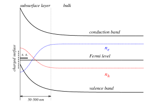
Band bending is a phenomenon that calls for considering models with the conductivity changing with the distance from the surface (at ). It is explained in many textbooks, e.g. Ref. Monch, , so we confine ourselves to a succinct resume in terms of a self-consistent calculation scheme, and we illustrate the main facts about it in Fig. 2. The phenomenon is due to surface states whose energy is determined in relation to bands, they may appear below the valence band, above the conductance band, or within the band gap. Assume there is no shift of the bands against the Fermi level at the surface. As such, the surface states accumulate a large electric charge. This gives rise to the creation of an electrostatic field that may be seen in the semiclassical (envelope) approximation of a shift of the band positions with respect to the Fermi level. But such shifts change the electric charge at the surface. In real crystals, we observe the surface Fermi level at the position arriving as a self-consistent solution of the problem sketched above. Thus, in equilibrium the semiconductor surface is slightly charged and is accompanied by an electrostatic field. Due to this field, the relative position of bands with respect to the Fermi level varies near the surface, and in this region the number of current carriers may be different from their bulk values. As indicated by eq. (3), a variation of the conductivity follows naturally. A similar model can also be found in Ref. Hoffmann, . More quantitative considerations allowing for band bending and carrier density profiles can be found in Ref. King, ; Multiscale, . We note, that treating band bending and current flow as independent phenomena is not entirely correct as both of these phenomena refer to the electrostatic potential. However, at sufficiently large distances from the current source, the current-associated field is so weak that it cannot substantially change the band bending. It is also not certain, if the above model is straightforwardly applicable to germanium. However, strong Fermi level pinning in germanium at the valence band is beyond any doubt APL .
IV Surface current from point source
IV.1 Transformation of the current equation
Now, we turn to eq. (2). We are interested in solving the equation in semi-space, i.e., with unrestricted two Cartesian coordinates and and the third one constrained to the upper semi-axis . As already mentioned, to take into account current sources and drains we need to modify eq. (2) by adding a source term. A common choice is the point-source. As such, we concentrate on the following equation,
| (4) |
To fully formulate the model, we state the boundary condition
| (5) |
which ensures that there is no current flowing through the plane . Eq. (4) is a linear equation and may be transformed to a familiar form of a Schrödinger operator if we switch from the function to a function defined by the relation
| (6) |
The resulting form of eq. (4) yields
| (7) |
Further, in the case of interest depends only on the coordinate. We shall use the representation of the Dirac delta in terms of eigenfunctions and eignenvalues of the operator . The eigenproblem factorizes, and in two dimensions ( and ) it is trivial. All complexity is in the one-dimensional equation
| (8) |
Now we study this equation, as both its eigenfunctions and eigenvalues appear in the solution of eq. (4) and (7). In analogy to the Schrödinger equation, we shall refer to the term
| (9) |
as the potential. If the potential vanishes, the corresponding eq. (8) is called potential-free. Noteworthy, the correspondence between the current equation and the time-independent Schrödinger equation is a formal feature, which will facilitate our reasoning. However, one should bear in mind, that the current flow equation we deal with is a classical theory of the electrostatic field, as shown in sect. III.1.
Transformation (6) mixes the electrostatic potential and the function . The boundary condition (5) then reads
| for | (10) | ||||
| for | (11) |
where is taken at .
IV.2 The potential
Eq. (8) binds the potential and the conductivity in a highly non-trivial way. To shed some light on its physical meaning we introduce a function
| (12) |
The function reflects how the conductivity, and hence the carrier density as implied by eq. (3), changes on the logarithmic scale. The potential can be rewritten in the following form
| (13) |
We observe, that the potential is independent of the absolute value of , i.e. multiplication of with any number does not alter the potential. As the potential contains terms with the first and second derivative of , the range of the change is important. A given potential value may be obtained for a small but abrupt change of as well as for a large deviation spread on a long distance. If the variation of is slow enough, the resulting potential is negligible. We assume it is the case for large as the bulk conductivity is well defined. The presence of the term appears to be slightly inconvenient from a physical standpoint. It requires accurate sampling of if it is to define a physical model. In this paper, we are interested in potentials that could be termed as small perturbations around the zero valued potential.
Fig. 3 and 4 show two potentials corresponding to two conductance profiles illustrating the formation of accumulation and depletion layers near the surface. As will be shown, physically relevant results are obtained if condition (10) is assumed. This is, however, at odds with the classical Monch and quantum King modeling of the carrier density. As such, these conductivity profiles do not appear as results of a theoretical calculation. A profile of approximately reproducing experimental data is given in Appendix C.
IV.3 Electrostatic potential at the surface
Not much can be said in general about solutions of eq. (4). In the potential-free case, the Green function may be calculated exactly, as shown in the Appendix B. However, we can infer a lot about the surface profile of the Green function,
where radial coordinate is introduced and the point source is located at . As shown in Appendix A, satisfies the following integral formula
| (14) |
where is the modified Bessel function of the second kind of zeroth order. This function explodes logarithmically at the origin and vanishes exponentially for large values of ; see Fig. 5. For the assumed potentials, the function is bounded and does not quickly vary. As such, the asymptotic behaviors of may be deduced from the above formula. Here we summarize the results elaborated in detail in Appendix A and informally explained in Fig. 5. At this point we do not care much about the multiplicative prefactor of . In sect. IV.4, we will set its normalization to suit the physical context. First, we report the short-range limit (), for which we have the following relation:
| (15) |
The same result would be obtained if there were a uniform conductivity in the whole sample. This is reasonable, as close to the source the current explores only a thin layer in the surface neighborhood where the conductivity can be considered constant. It is the behavior of for large that is important here.
There are two asymptotic relations for large depending on whether condition (10) or (11) is considered. For (10) we can assume, that , and then
| (16) |
where corresponds to the bulk value of the conductivity, . It is a very intriguing fact, that the asymptotic values of conductivity are given by its surface and bulk values, no matter how complicated the conductivity profile beneath the surface is.
The second boundary condition (11) gives rise to a modified behavior at large distances if . The case of negative is not treated here for the bound state it has in the spectrum (for more details see Appendix A). We do not know any experimental results demonstrating such a quick voltage drop on the surface. This is why it appears to be a hint as to how the conductivity should be modeled close to surfaces. Noteworthy, numerical algorithms often deal with thin slices of constant conductivity spa2 ; voigtlander parallel to the surface. As such, they assume condition (5).
IV.4 Effective surface conductivity
The asymptotic description obtained for the condition (10) motivates introducing a function which is defined as
| (17) |
To justify this definition, we write the electrostatic potential in an infinitesimal range around the source,
| (18) |
where is the current supplemented. In this way we get a normalization factor for the whole range of . As a consequence of eq. (14) one can write the following for any and
| (19) |
For small both eq. (15) and (18) hold. They may be plugged into the above formula resulting in the relation
| (20) |
Thus, may be viewed as an effective surface conductivity. It reflects the fact that the measured surface conductivity varies with the distance from the source due to changes in the conductivity below.
Fig. 6 and 7 show the effective conductivity obtained for the potentials shown in Fig. 3 and 4. The results come from numerical integration of eq. (14) with numerically calculated functions .
V Beyond the point-source approximation
A more realistic model of the contact supplying the current to the sample involves an area on the surface, where both the function and the current are given. This corresponds to the physical situation in which the potential and current at the contact are determined by the supplying electrodes. A detailed analysis of the problem goes beyond the scope of the present article. While the experimental data were acquired with different tips, yielding different contact areas and shapes, the results seem not to depend on them. This is why we will be satisfied with only a few general remarks.
The requirement that for a given area be equal to a predefined function, can be satisfied by making use of the obtained Green function. For a qualitative discussion one can formulate an analogue of the multipole expansion known in electrostatics to arrive at quickly vanishing () terms.
To take into account the incoming current profile, further developments are needed. We observe that the current density corresponds, upon transformation (6), to the quantity
Assuming boundary condition (10) we can draw an analogy to the quantum mechanics and interpret the current density at the surface as the momentum of the incoming particles. This makes it clear that for different we can get different penetration depths, and hence different solutions. The Green function is built as a weighted sum of all related eigenfunctions, the larger the eigenvalue (energy) the smaller the weight. Thus, the point-source formula is dominated by low-energy features. As we have observed, it is the long-ranged behavior () that is governed by small eigenvalues (). Regions that are distant enough should not be affected either by source finite-size effects or by the value of the current density.
VI Conclusions
Our experimental data show a systematic change of the surface conductivity with the distance between the probes. To understand the results we have investigated the classical current flow equation. We have developed a theoretical scheme making it evident that the change of the conductivity beneath the surface impacts the results obtained on the surface, i.e. the well-known formula for the current point-source is to be transformed to the form . Asymptotic values of have been found to be the actual value close to the source and the bulk value far from the source. This scheme eases the numerical effort needed to obtain the surface conductivity profile. Furthermore, it delivers a framework to discuss and classify different effects obtained in numerical studies such as that in Ref. Hoffmann, . We have confined our considerations to small deviations of the conductance parameter.
There are several interesting open questions mentioned in the text, however three issues are of practical interest. First, the inverse problem, i.e. the existence of a scheme of surface measurements allowing for reconstruction of the conductivity profile. Second, capturing the mechanism behind the dimensional reduction Hoffmann ; APL seems both interesting and feasible. Third, apparently the condition corresponds to physical observations. It is at odds with the way (envelope) wavefunctions are modeled near the surface King . This contradiction needs to be clarified.
VII Acknowledgements
Founding for this research has been provided by EC under the Large-scale Integrating Project in FET Proactive of the 7th FP entitled “Planar Atomic and Molecular Scale devices” (PAMS). The research was carried out with equipment purchased thanks to the financial support of the European Regional Development Fund in the framework of the Polish Innovation Economy Operational Program (contract no. POIG.02.01.00-12-023/08).
Appendix A Calculation Details
Here we describe in more detail the calculations behind the results outlined in sect. IV. To begin with, we write explicitly eq. (7) which is to be solved.
| (21) |
where the potential is calculated from the conductivity function
The solution of eq. (21) defines the Green function for the differential operator. There are many methods of finding Green functions, from which spectral decomposition Green1 ; Green2 is most appropriate to us. We observe that the related eigenproblem is solved via
| (22) |
where we follow notation introduced in sect. IV. Both and are any real numbers, while may be considered positive.
The Green function may be expressed as
| (23) |
we consider real , so . The eigenmodes have to obey a uniform normalization condition, e.g.
Using relation A5 from Ref. k0,
we can integrate out and to arrive at the most important formula in this paper
| (24) |
where and stands for the modified Bessel function of the second kind. To proceed, the functions and related eigenvaues are needed. This can be done for the potential-free case as shown below (see Appendix B).
With no harm to generality we set and . As the point source is to be located at the surface, we also set . We look for the surface profile of the Green function, hence we can also put . The function corresponds to the sought-after surface profile . Now we can argue for the asymptotic formulas given in sect. IV. The integral to solve is
| (25) |
Substituting , the integral becomes
| (26) |
We note that the Bessel function has a logarithmic divergence at the origin and exponentially decays for large arguments. Integrating gives
see 11.4.23 in Ref. abra, . As the function is bounded, for any desired accuracy one can find a value , for which
| (27) |
As a consequence, we can switch to integration over a finite interval.
First we deal with the case of small values of . To this end, we observe that for sufficiently large the potential may be considered a small perturbation of the eigenstate obtained for the potential-free equation. As such, and . Hence, there is an argument such that for any it holds that . As such, we can split integration into two parts,
| (28) |
The first term vanishes due to shrinking of the integration interval with and finally we are left with the limiting value
| (29) |
Now, we address large values of . We assume that the limit
is finite and does not vanish. Hence, there is again such that for any the difference can be neglected. Then
| (30) |
Now it is the second term which vanishes due to reduction of the integration interval. As such we arrive at the limiting value
| (31) |
It is easy to note, that eq. (8) has an zero eigenvalue corresponding to the function . This function is related to the freedom left by eq. (2), which admits shifting its solutions by any constant. The second independent solution assuming reads
It vanishes for but has a non-vanishing first derivative. Following the theorems on continuity of solutions of a differential equation with respect to a parameter ode we make use of the solution to arrive at
| (32) |
where the denominator appears due to the proper normalization.
To complete the discussion, we address the case, where for and (see eq. (37)). In such a case we arrive at the following relation
| (33) |
where stands for the maximal argument, for which the linear approximation may be considered exact. As a consequence, we obtain the relation
| (34) |
with a different asymptotic current behavior. The numerical value of the integral above yields
as can be interfered from formula 11.4.22 in Ref. abra, . The case with a negative value of is more complicated. The spectrum then has an isolated eigenfunction with a negative eigenvalue adjoint and hence the Green function becomes more complicated than the functions considered here.
It is evident from the numerical examples described in sect. IV, that changes on a slightly larger scale than the potential. To remark on finding solutions of eq. (8) for small eigenvalues , we denote the range of the potential with . It corresponds to the distance from which the potential may be neglected. Then, in the basis of the matrix element reads
| (35) |
For small values of and the integral tends to the value
| (36) |
if in the range functions can be considered constant. As such, the vectors obeying the inequality
may be considered small. This hints at the length scale needed to solve the problem numerically – to explore the lowest eigenvalue sector one needs to work on segments in length. We used the standard Mathematica 10 routines to diagonalize the operator (with higher precision). The segment lengths that we explore are about 20 000 nm and 40 000 nm. The lowest eigenvalues turned numerically unstable. This is why we excluded several lowest eigenvalues. was found by extrapolation a function obtained as quadratic interpolation of for several lowest remaining eigenvalues. As shown in Fig. 6 and 7, the results are close to the exact values . A more credible and efficient approach to finding is to solve eq. (8) for different values of with the boundary condition (10) on a segment larger than the range of the potential . The normalization requires then, that there is a given amplitude of oscillations for all solutions in the potential-free region.
Appendix B Green functions for the potential-free equation
For the potential-free case the eigenfunctions for the eigenvalues values yield if condition (10) is to be satisfied and if condition (11) holds. The phase shift is given by the formula
| (37) |
where denotes and is the sign of . For eigenfunctions we can complete the integration in eq. (24) to arrive at the following formula
| (38) |
Using relation 11.4.14 in Ref. abra, we obtain
| (39) |
which reduces to the familiar formula at the surface. The term with appears due to the boundary conditions to ensure that no current escapes through the surface. Similar Green functions are known in electrostatics to give rise to image charges.
We note that eigenfunctions converge to a constant in the limit , which solves potential-free eq. (8) with . This is a demonstration of theorems on the continuity of solutions of a differential equations with respect to parameters.
Appendix C Experimental data revisited
The insight gained from the above analysis of the current flow equation prompts a few comments on the experimental data presented in sect. II. The bulk value of the conductivity appears different for the two samples investigated and reads about cm-1 and cm-1 for sample A and B, respectively. In both cases it is below the nominal value. The experimental conductivity decreases with the distance from the source, see Fig. 1. The trend is reproduced in Fig. 6, which suggests an enhancement of the conductivity at the surface. For the p-type doped samples the surface Fermi level is located close to the valence band and hence the formation of an accumulation layer consistently explains the data.
In Fig. 6 and 7 we observe, that the first derivative of vanishes for . As such, the following asymptotic expansion for large
| (40) |
is natural. We stop at the first correction term and rewrite the above formula using an effective parameter
| (41) |
One should bear in mind, that the terms neglected in eq. (40) can be important if the term with becomes relevant. Hence, some caution is needed when attributing a physical meaning to .
To apply the expression (41) to the experimental setup described in Ref. APL, we put the point current source at the point and the drain at and calculate the voltage drop between probes located at and . Here the parameter corresponds to the parameter in Ref. APL, . The resulting formula for the measured resistance , i.e. the voltage drop between and divided by the current supplemented to the sample, is poorly informative. However, it is interesting to expand it in powers of
| (42) |
We confine our considerations to the two lowest orders of expansion written above. For close to zero they are finite, thus the first term (of the order ) dominates. At this level, the scaling behavior characteristic for three dimensions APL may be seen: the quantity does not depend on . In the case of experimental data such a universality is clearly observed for equal to 8 and 16 m, see Fig. 8. For smaller the second term () spoils the universality. The reason is, that for close to unity, both terms on the right-hand side of eq. (42) are singular. The second one explodes quicker and dominates for big enough , no matter how large is. As the second term in eq. (42) is due to the subsurface variation of the conductivity, the deviations from the universal behavior bear information about the subsurface region.
| D | Sample A | Sample B | |||
|---|---|---|---|---|---|
| [] | Ge(001) | Ge(001):H | SEM irr. | Ge(001) | Ge(001):H |
| 2 | 1.87 / 8.64 | 1.87 / 8.64 | 2.30 / 3.97 | 1.50 / 1.03 | 1.93 / 2.65 |
| 4 | 1.73 / 7.53 | 1.73 / 7.53 | 2.05 / 4.97 | 1.66 / 2.90 | 1.55 / 4.34 |
| 8 | 1.55 / 5.84 | 1.55 / 5.84 | 1.75 / 6.59 | 1.75 / 3.83 | 1.42 / 7.27 |
| 16 | 1.47 / 17.1 | 1.47 / 17.1 | 1.47 / 12.4 | 1.19 / 40.8 | 1.20 / 22.4 |
The formula assuming (41) for was used to fit the experimental data for both samples, see Tab. 2. As a result, estimated values of vary much less than for a naive fit behind numbers presented in Tab. 1. The values of are usually of the same order, and no clear trend is seen, which is probably due to the higher order terms.
Dimensional analysis allows to identify a length parameter
a characteristic distance where surface corrections are important. In our case, it appears about 150-500 nm. This is consistent with the profile we apply to reproduce our experimental data, see Fig. 8. We use the following function to model conductivity changes
| (43) |
where , and are parameters adjusted to the experimental data. This function satisfies the boundary condition (10) and it decays exponentially except for a region close to the surface. As such, it a reasonable model describing screening of the surface charge Monch . The parameters and have physical meaning while depends on the way one solves the problem (applied normalization condition). As shown in Fig. 8 simulated data for nm and satisfactorily correlate with the experimental points. Similar results can be obtained for ranging between 80 and 200 nm and for between 3 and 7. Interpretation of these parameters within the band bending theory, e.g. the Schottky approximation, seems to be misleading as it overestimates the doping and underestimates the band-bending.
References
- (1) Ph. Hofmann and J. W. Wells, J. Phys.: Condens. Matter 21 013003 (2009).
- (2) S. Hasegawa, I. Shiraki, T. Tanikawa, Ch. L. Petersen, T. M. Hansen, P. Boggild and F. Grey, J.Phys.: Condens. Matter 14, 8379 (2002)
- (3) G. Scappucci, G. Capellini, W. M. Klesse, and M. Y. Simmons, Nanoscale 5, 2600 (2013).
- (4) B. V. C. Martins, M. Smeu, L. Livadaru, H. Guo, and R. A. Wolkow, Phys. Rev. Lett. 112, 246802 (2014).
- (5) Z. Korczak, T. Kwapiński and P. Mazurek, Surf. Sci. 604, 54 (2010).
- (6) J. W. Wells, J. F. Kallehauge, T. M. Hansen and Ph. Hofmann, Phys. Rev. Lett. 97, 206803 (2006).
- (7) E. Perkins, L. Barreto, J. Wells and Ph. Hofmann, Rev. Sci. Instrum. 84, 033901 (2013)
- (8) S. M. Hu, J. Appl. Phys. 53, 1499 (1982)
- (9) S. T. Dunham, N. Collins and N. Jeng, J. Vac. Sci. Technol. B 12, 283 (1994)
- (10) L. S. Tan, L. C. P. Tan, M. S. Leong, R. G. Mazur and C. W. Ye, J. Vac. Sci. Technol. B 20, 483 (2002)
- (11) M. Wojtaszek, J. Lis, R. Zuzak, B. Such and M. Szymonski, Appl. Phys. Lett. 105, 042111 (2014)
- (12) M. Kolmer, S. Godlewski, H. Kawai, B. Such, F. Krok, M. Saeys, Ch. Joachim, and M. Szymonski, Phys. Rev. B 86, 125307 (2012).
- (13) H. Seo, R. C. Hatch, P. Ponath, M. Choi, A. B. Posadas, and A. A. Demkov, Phys. Rev. B 89, 115318 (2014)
- (14) E. Landemark, C. J. Karlsson, L. S. O. Johansson, and R. I. G. Uhrberg, Phys. Rev. B 49, 16523 (1994).
- (15) L. D. Landau and E. M. Lifshitz, Electrodynamics of Continuous Media Pergamon Press Ltd., 1963, Chap. III
- (16) An-Ping Li, K. W. Clark, X.-G. Zhang and A. P. Baddorf Adv. Funct. Mater. 23, 2509 (2013)
- (17) S. M. Sze and K. K. Ng, Physics of Semiconductor Devices John Wiley & Sons, Inc., Hoboken, New Jersey, 2007.
- (18) W. Monch, Semiconductor Surfaces and Interfaces Springer, Berlin, New York, 2001.
- (19) P. D. C. King, T. D. Veal, C. F. McConville, Phys. Rev. B 77, 125305 (2008).
- (20) S. Just, M. Blab, S. Korte, V. Cherepanov, H. Soltner, B. Voigtländer, Phys. Rev. Lett. 115, 066801 (2015) (arXiv:1505.01288)
- (21) O. Sinai, O. T. Hofmann, P. Rinke, M. Scheffler, G. Heimel and L. Kronik, Phys. Rev. Lett. B 91, 075311 (2015).
- (22) G. W. Hanson, A. B. Yakovlev, Operator Theory for Electromagnetics: An Introduction Springer, New York, 2002
- (23) George B. Arfken and Hans J. Weber Mathematical Methods for Physicists, sixth edition, Elsevier Academic Press, 2005; section 11.2.
- (24) Youn-Sha Chan, L. J. Gray, T. Kaplan, Glaucio H. Paulino, Proceedings: Mathematical, Physical and Engineering Sciences, Vol. 460, No. 2046 (Jun. 8, 2004), pp. 1689-1706
- (25) M. Abramowitz and I. A. Stegun, Handbook of Mathematical Functions, Tenth Printing, 1972
- (26) W. G. Kelley, A. C. Peterson, The Theory of Differential Equations, Springer-Verlag New York 2010, chapt. 8.7
- (27) G. Bonneau, J. Faraut and G. Valent, Am. J. Phys. 69, 322 (2001).