Magneto-transport study of top- and back-gated LaAlO3/SrTiO3 heterostructures
Abstract
We report a detailed analysis of magneto-transport properties of top- and back-gated LaAlO3/SrTiO3 heterostructures. Efficient modulation in magneto-resistance, carrier density, and mobility of the two-dimensional electron liquid present at the interface is achieved by sweeping top and back gate voltages. Analyzing those changes with respect to the carrier density tuning, we observe that the back gate strongly modifies the electron mobility while the top gate mainly varies the carrier density. The evolution of the spin-orbit interaction is also followed as a function of top and back gating.
The two-dimensional electron liquid (2DEL) present at the interface between the insulating oxides LaAlO3 (LAO) and SrTiO3 (STO) exhibits several fascinating properties, including superconductivity and a large spin-orbit coupling.Mannhart and Schlom (2010) It has also attracted much attention in the context of device applications following the realization of field-effect transistors and devices with nanoscale dimensions.Zubko et al. (2011); Förg et al. (2012); Cen et al. (2009); Stornaiuolo et al. (2012, 2014)
The large electric permittivity of the STO substrate, especially at low temperatures, facilitates tuning of the 2DEL properties by an electric field effect in back gate transistors.Zubko et al. (2011) This back gate configuration allows considerable control of multiple parameters of the 2DEL such as the superconducting critical temperature, spin-orbit interaction, carrier density, and mobility.Caviglia et al. (2008); Bell et al. (2009); Caviglia et al. (2010); Ben Shalom et al. (2010a); Joshua et al. (2012); Rakhmilevitch et al. (2013) Additionally, it might simultaneously change the confinement of the 2DEL.Bell et al. (2009); Minohara et al. (2014); Biscaras et al. (2014) This confinement modifies the bulk STO electronic structure and leads to an orbital ordering with light and heavy / sub-bands. Popović et al. (2008); Salluzzo et al. (2009) Recently, there has been growing interest in employing top electrodes in gating experiments of LAO/STO devices,Li et al. (2011); Bi et al. (2014); Hosoda et al. (2013); Eer ; Bal et al. (2014); Goswami et al. (2015) as LAO has a large band gap and reasonably large dielectric constant.Edge et al. (2006) The transistor operation of a top-gated LAO/STO device was demonstrated with an on-off switch of the conductivity using less than 1 V.Förg et al. (2012) However, the responses of the 2DEL to top and back gate can be different: a first comparison revealed, indeed, a different modulation of the mobility by the two approaches.Hosoda et al. (2013)
In this paper, we present a systematic study of transport properties of top- and back-gated LAO/STO heterostructures in the presence of a perpendicular magnetic field. Electric field effect tuning is achieved by using the LAO film and STO substrate as top and back gate dielectrics respectively. Large tunability in resistance, carrier density and magneto-resistance were observed in both configurations. The top-gate approach shows reversible tuning with voltage sweeping, contrary to back gate.Caviglia et al. (2008); Biscaras et al. (2014) Top and back gates affect the mobility differently, back gate being more effective to boost it. The evolution of the weak-localization/weak-antilocalization behavior is also extracted from the magneto-transport data. This allows us to study inelastic and spin-orbit magnetic fields for constant carrier densities achieved by a combined use of top and bottom gates. We try to link the differences in the response of the 2DEL to the confining potential shape and to the multi-band conduction.
The Hall bars are defined by pre-depositing an amorphous STO layer as a hard mask.Stornaiuolo et al. (2012) Structures down to 25 m in width are realized by optical lithography. Subsequently, epitaxial LAO films are deposited on TiO2-terminated STO (001)-oriented single crystals by pulsed laser deposition in an oxygen pressure of Torr at 800 or 830 and annealed in 0.2 bar of oxygen at 520 for an hour as documented elsewhere.Caviglia et al. (2008); Cancellieri et al. (2010) After growth, ex-situ sputtered Pt is used for the top gate and Au films are sputtered on the backside of the substrate for the back gate electrodes. A schematic of a device with a top and back gate is displayed in Figure 1(a). Figure 1(b) shows an optical image of a typical Hall bar structure with sputtered Pt film as the top gate. Measurements are carried out keeping the leakage current from the top electrode below 1 nA, much smaller than the channel current (typically in the range 0.1 1 A). Transport data presented here below were obtained measuring a sample grown at 830 with 15 unit cells (u.c.) thick crystalline LAO in a perpendicular magnetic field configuration. Samples with thickness in the range 10 17 u.c. and channel width in the range 25 100 m were also fabricated and tested: they all show comparable transport properties.
Capacitance characterization with an AC voltage of 10 mV at 200 Hz demonstrates good capacitor behavior (small loss tangent and negligible leakage current) of top-gated devices prepared in this fashion.vac We consistently observe an effective dielectric constant () for the Pt/LAO/2DEL capacitor smaller than the bulk value, which is possibly due to interfacial effects.Stengel and Spaldin (2006) Moreover, this interfacial effect might be the reason for the weak dependence of on temperature as shown in Figure 1(c) (bulk LAO has a temperature independent dielectric constant). has little dependence on the top gate voltage as shown in Figure 1(d). We also do not observe in the investigated range substantial changes in the capacitance when we modulate the 2DEL carrier density using back gate.cap
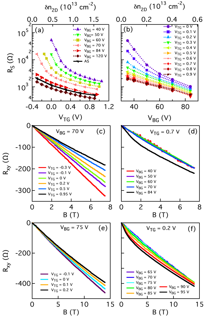
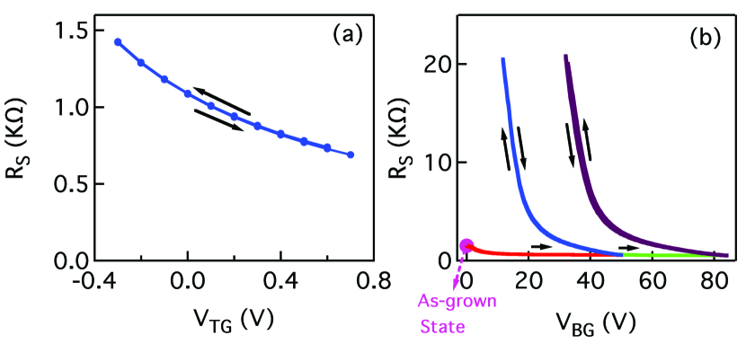
Figure 2 compares the low temperature resistance behavior sweeping the gate voltages from the top (panel (a)) and from the back (panel (b)).sam For top gate voltages , the tuning of the sheet resistance is reversible. We note the modulation of is about 40%, the range being set to avoid leakage across the LAO layer. For back gate voltages , a large history dependent behavior manifests in when is first swept upwards and then downwards. In this geometry, from the as-grown state, first decreases and then saturates for a wide range of (red curve in panel (b)). If we stop increasing (at = 50 V as in panel (b)) and reverse the sweeping direction, we observe that the resistance increases strongly (blue curve), deviating from the upward sweep. Then, as long as is kept below , the sweeps are reversible (the resistance moves along the blue curve). In this configuration, extremely high resistance states can be achieved. If exceeds , the resistance remains constant in the upward sweep (green curve); however, the new reversible behavior is shifted to higher voltages (purple curve). This “forming process” of the resistance state suggests that many added electrons spill out of the quantum well and go into trapped states.Biscaras et al. (2014)
To build a more comprehensive understanding of the different effects of and , we investigate the magneto-transport properties of the 2DEL using both gates. The data are displayed in Figure 3: in the left panels, the measurements are performed at various while is maintained fixed, and vice versa for the right panels. We observe that the changes in induced by sweeping or are quite comparable, but on a completely different voltage range. Figures 3(c) - 3(f) display the Hall resistance as a function of magnetic field for different values of and : we observe an evolution from linear to non-linear behavior pointing to a transition from single to multiple band conduction.Ben Shalom et al. (2010b); Joshua et al. (2012); Fête et al. (2012) Since correctly extracting the total carrier density from a non-linear is generally difficult, the modulation of the total carrier density is calculated using a parallel plate capacitor model. For the top gate, using = 12, we obtain a change in that agrees with the estimation from the variation of the Hall coefficient with when is linear in field (see Figure 3(c)). For the back gate, is obtained by the capacitor measurement as a function of .Caviglia et al. (2008) These modulations are plotted as top axes in panels (a) and (b). Now comparing the change in versus for the two gates, we see that the same modulation is achieved by top gate with a variation in that is roughly twice that obtained with the back gate.
This different response of to the top and back gates, as well as the evolution of the Hall effect, may suggest distinct effects of the two gates on the confining potential and hence on the sub-band structure. Self-consistent calculations using a Schrdinger-Poisson approach show that a pure increase in carrier density results in a stronger confinement.Copie et al. (2009); Khalsa and MacDonald (2012) Modeling of back gate transistors Bell et al. (2009) and analysis of back gate voltage sweeps Biscaras et al. (2014) indicate that positive voltages increase the confinement width (weaker confinement) of the 2DEL; as a consequence, the energy splitting between the lower energy - and lower mobility - and higher energy / - and higher mobility - bands should be reduced.
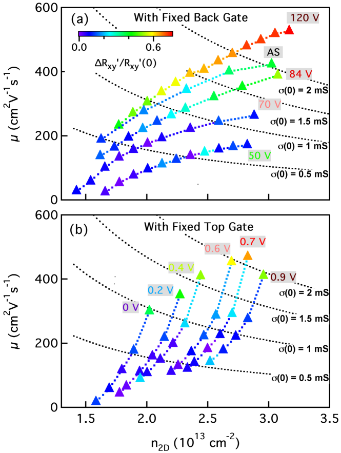
In order to highlight the difference between the two gate approaches, we plot the mobility as a function of the carrier density in Figure 4 for top (panel (a)) and back (panel (b)) gate voltage sweeps. is estimated from the linear Hall effect and the carrier change induced by the capacitor effect, and is defined as , where is the electron charge and is the zero-field conductance; calculated in this fashion is therefore an effective mobility. In the same graphs, we use a color code to indicate the degree of non-linearity observed in the Hall resistance , being the derivative at a given field. For single band conduction, is zero (represented as blue) while for multi-band conduction, it becomes non-zero (represented as yellow/red). The mobility curves in Figure 4(a) show that top gate sweeps result in a strong modulation of and a smaller change in . When we change the back gate voltage, we notice a sharp increase in the carrier mobility: this is more evident in panel (b) where mobility is strongly enhanced by back gate voltages for a small variation in the carrier density. We also observe that, concomitant with the increase in , the Hall resistance becomes non-linear, suggesting that a second band with high mobility comes into play. Popović et al. (2008); Salluzzo et al. (2009); Ben Shalom et al. (2010b); Joshua et al. (2012); Fête et al. (2012)
A possible scenario to understand the response of the transport properties to the field-effect tuning relates the effect of the two gates to the confining potential. As discussed above, a deconfinement of the 2DEL would reduce the versus / band splitting, this energy becoming negative in bulk STO. Allen et al. (2013) Along with this effect, carriers could be transferred to the more mobile band, resulting in higher mobility and non-linear Hall resistance. On the other hand, if electrons are more confined, the energy splitting should increase, and a shift in the Fermi level would mainly induce an increase in with little change in .
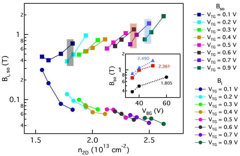
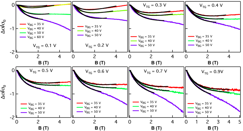
We finally explore the effect of top and back gates on the spin-orbit interaction of the system. We fit the magneto-conductance curves using the Maekawa-Fukuyama formula Maekawa and Fukuyama (1981) and extract the inelastic field and the spin-orbit field for different sets of and .SI Figure 5 shows the evolution of and as a function of . We observe that for each the back-gate tuning results in an effective modulation of , in agreement with previous studies on the spin-orbit interaction.Caviglia et al. (2010); Fête et al. (2012) While seems to be determined mainly by , should be more sensitive to the modification of the confining potential. To get further insight into the evolution of upon gate tuning, in the inset of Figure 5, we plot versus for the three carrier densities indicated by the shaded areas in the main panel of the figure. For the plot, is chosen as the “tuning parameter” as it should affect the electron confining potential most and hence the strength of the spin-orbit interaction, although probably in a complex way.Joshua et al. (2012); Zhong et al. (2013); Kim et al. (2013); Khalsa et al. (2013) The data plotted in the inset show that the spin-orbit coupling can be tuned at constant and suggest that is indeed modifying the confinement of the 2DEL.
To conclude, we present a systematic study of the effects of top and back gate on LAO/STO heterostructures. The detailed characterization reveals differences between the evolution of , and magneto-conductance using the two approaches. The observation for the back gate of a forming process and the strong enhancement of the electron mobility suggest that positive back gate deconfines the 2DEL: on one side some electrons are trapped deep in the STO; on the other side, the contribution from / states becomes more significant. The control of the electronic properties of the 2DEL using both gates, as demonstrated here, allows the spin-orbit strength to be tuned at fixed carrier densities and opens new opportunities to realize transistors where mobility and carrier density are tuned independently.
We acknowledge Pavlo Zubko for useful experimental advice and Marc Gabay for enlightening discussions. We thank M. Lopes and S. C. Mller for the technical assistance. This research was supported by the Swiss National Science Foundation through the NCCR MaNEP and Division II and has received funding from the European Research Council under the European Unionʼs Seventh Framework Programme (FP7/2007–2013) / ERC Grant Agreement no. 319286 (Q-MAC).
I SUPPLEMENTARY MATERIAL
In this supplementary information, we fit the magneto-conductance curves using the Maekawa-Fukuyama (MF) formula:Maekawa and Fukuyama (1981); Caviglia et al. (2010)
where with the digamma function, and . Here and is a universal value of conductance.
Figure 6 displays magneto-conductance curves. In each panel, the top gate is fixed and the back gate is varied. For low doping samples, the data seem to reflect the evolution of the weak-localization/weak-antilocalization behavior as reported in references 9 and 10. At high dopings and high magnetic fields, data deviate from weak anti-localization fittings, making the estimation of the fitting parameters less reliable.Yuan et al. (2013)
References
- Mannhart and Schlom (2010) J. Mannhart and D. Schlom, Science 327, 1607 (2010).
- Zubko et al. (2011) P. Zubko, S. Gariglio, M. Gabay, P. Ghosez, and J.-M. Triscone, Annu. Rev. Condens. Matter Phys. 2, 141 (2011).
- Förg et al. (2012) B. Förg, C. Richter, and J. Mannhart, Appl. Phys. Lett. 100, 053506 (2012).
- Cen et al. (2009) C. Cen, S. Thiel, J. Mannhart, and J. Levy, Science 323, 1026 (2009).
- Stornaiuolo et al. (2012) D. Stornaiuolo, S. Gariglio, N. J. G. Couto, A. Fête, A. D. Caviglia, G. Seyfarth, D. Jaccard, A. F. Morpurgo, and J.-M. Triscone, Appl. Phys. Lett. 101, 222601 (2012).
- Stornaiuolo et al. (2014) D. Stornaiuolo, S. Gariglio, A. Fête, M. Gabay, D. Li, D. Massarotti, and J.-M. Triscone, Phys. Rev. B 90 (2014).
- Caviglia et al. (2008) A. D. Caviglia, S. Gariglio, N. Reyren, D. Jaccard, T. Schneider, M. Gabay, S. Thiel, G. Hammerl, J. Mannhart, and J.-M. Triscone, Nature 456, 624 (2008).
- Bell et al. (2009) C. Bell, S. Harashima, Y. Kozuka, M. Kim, B. G. Kim, Y. Hikita, and H. Y. Hwang, Phys. Rev. Lett. 103, 226802 (2009).
- Caviglia et al. (2010) A. D. Caviglia, M. Gabay, S. Gariglio, N. Reyren, C. Cancellieri, and J.-M. Triscone, Phys. Rev. Lett. 104, 126803 (2010).
- Ben Shalom et al. (2010a) M. Ben Shalom, M. Sachs, D. Rakhmilevitch, A. Palevski, and Y. Dagan, Phys. Rev. Lett. 104, 126802 (2010a).
- Joshua et al. (2012) A. Joshua, S. Pecker, J. Ruhman, E. Altman, and S. Ilani, Nat. Commun. 3, 1129 (2012).
- Rakhmilevitch et al. (2013) D. Rakhmilevitch, I. Neder, M. B. Shalom, A. Tsukernik, M. Karpovski, Y. Dagan, and A. Palevski, Phys. Rev. B 87, 125409 (2013).
- Minohara et al. (2014) M. Minohara, Y. Hikita, C. Bell, H. Inoue, M. Hosoda, H. Sato, H. Kumigashira, M. Oshima, E. Ikenaga, and H. Hwang, arXiv:1403.5594 (2014).
- Biscaras et al. (2014) J. Biscaras, S. Hurand, C. Feuillet-Palma, A. Rastogi, R. Budhani, N. Reyren, E. Lesne, J. Lesueur, and N. Bergeal, Scientific reports 4 (2014).
- Popović et al. (2008) Z. Popović, S. Satpathy, and R. Martin, Phys. Rev. Lett. 101, 256801 (2008).
- Salluzzo et al. (2009) M. Salluzzo, J. C. Cezar, N. B. Brookes, V. Bisogni, G. M. De Luca, C. Richter, S. Thiel, J. Mannhart, M. Huijben, A. Brinkman, et al., Phys. Rev. Lett. 102, 166804 (2009).
- Li et al. (2011) L. Li, C. Richter, S. Paetel, T. Kopp, J. Mannhart, and R. Ashoori, Science 332, 825 (2011).
- Bi et al. (2014) F. Bi, M. Huang, S. Ryu, H. Lee, C.-W. Bark, C.-B. Eom, P. Irvin, and J. Levy, Nat. Commun. 5, 5019 (2014).
- Hosoda et al. (2013) M. Hosoda, Y. Hikita, H. Y. Hwang, and C. Bell, Appl. Phys. Lett. 103, 103507 (2013).
- (20) P. Eerkes, W. van der Wiel, and H. Hilgenkamp, Appl. Phys. Lett. 103, 201603 (2013); P. Eerkes, PhD thesis (2014), http://dx.doi.org/10.3990/1.9789036536554.
- Bal et al. (2014) V. V. Bal, M. M. Mehta, S. Ryu, H. Lee, C. M. Folkman, C.-B. Eom, and V. Chandrasekhar, arXiv:1407.5939 (2014).
- Goswami et al. (2015) S. Goswami, E. Mulazimoglu, L. M. Vandersypen, and A. D. Caviglia, Nano Lett. DOI: 10.1021/acs.nanolett.5b00216 (2015).
- Edge et al. (2006) L. Edge, D. Schlom, P. Sivasubramani, R. Wallace, B. Hollander, and J. Schubert, Appl. Phys. Lett. 88, 112907 (2006).
- Cancellieri et al. (2010) C. Cancellieri, N. Reyren, S. Gariglio, A. D. Caviglia, A. Fête, and J.-M. Triscone, Europhys. Lett. 91, 17004 (2010).
- (25) We note that keeping the samples in a vacuum environment after lithography and before Pt sputtering improves the dielectric response of the top-gated heterostructures.
- Stengel and Spaldin (2006) M. Stengel and N. A. Spaldin, Nature 443, 679 (2006).
- (27) As shown by Li et al. in reference 17, the top gate capacitance changes when one reaches the strong depletion regime.
- (28) Data were obtained from different patterns of the same sample.
- Ben Shalom et al. (2010b) M. Ben Shalom, A. Ron, A. Palevski, and Y. Dagan, Phys. Rev. Lett. 105, 206401 (2010b).
- Fête et al. (2012) A. Fête, S. Gariglio, A. D. Caviglia, J.-M. Triscone, and M. Gabay, Phys. Rev. B 86, 201105 (2012).
- Copie et al. (2009) O. Copie, V. Garcia, C. Bödefeld, C. Carrétéro, M. Bibes, G. Herranz, E. Jacquet, J.-L. Maurice, B. Vinter, S. Fusil, et al., Phys. Rev. Lett. 102, 216804 (2009).
- Khalsa and MacDonald (2012) G. Khalsa and A. MacDonald, Phys. Rev. B 86, 125121 (2012).
- Allen et al. (2013) S. J. Allen, B. Jalan, S. Lee, D. G. Ouellette, G. Khalsa, J. Jaroszynski, S. Stemmer, and A. H. MacDonald, Phys. Rev. B 88, 045114 (2013), URL http://link.aps.org/doi/10.1103/PhysRevB.88.045114.
- Maekawa and Fukuyama (1981) S. Maekawa and H. Fukuyama, J. Phys. Soc. Jpn. 50, 2516 (1981).
- (35) See supplementary information for magneto-conductance curves for back gate voltage sweeps, estimated and as a function of carrier density, and the relation between and .
- Zhong et al. (2013) Z. Zhong, A. Tóth, and K. Held, Phys. Rev. B 87, 161102 (2013).
- Kim et al. (2013) Y. Kim, R. M. Lutchyn, and C. Nayak, Phys. Rev. B 87, 245121 (2013).
- Khalsa et al. (2013) G. Khalsa, B. Lee, and a. H. MacDonald, Phys. Rev. B 88, 041302 (2013).
- Yuan et al. (2013) H. Yuan, M. S. Bahramy, K. Morimoto, S. Wu, K. Nomura, B.-J. Yang, H. Shimotani, R. Suzuki, M. Toh, C. Kloc, et al., Nat. Phys. 9, 563 (2013).