22email: sergio.coelho@up.ac.za 33institutetext: J.F.R. Archilla 44institutetext: Group of Nonlinear Physics, Universidad de Sevilla, ETSII, Avda Reina Mercedes s/n, 41012-Sevilla, Spain, 44email: archilla@us.es 55institutetext: F.D. Auret 66institutetext: Department of Physics, University of Pretoria, Lynnwood Road, Pretoria 0002, South Africa,
66email: danie.auret@up.ac.za 77institutetext: J.M. Nel 88institutetext: Department of Physics, University of Pretoria, Lynnwood Road, Pretoria 0002, South Africa,
88email: jackie.nel@up.ac.za
S.M.M. Coelho, J.F.R. Archilla, F.D. Auret and J.M. Nel
The origin of defects induced in ultra-pure germanium by Electron Beam Deposition
Abstract
The creation of point defects in the crystal lattices of various semiconductors by subthreshold events has been reported on by a number of groups. These observations have been made in great detail using sensitive electrical techniques but there is still much that needs to be clarified. Experiments using Ge and Si were performed that demonstrate that energetic particles, the products of collisions in the electron beam, were responsible for the majority of electron-beam deposition (EBD) induced defects in a two-step energy transfer process. Lowering the number of collisions of these energetic particles with the semiconductor during metal deposition was accomplished using a combination of static shields and superior vacuum resulting in devices with defect concentrations lower than cm-3, the measurement limit of our deep level transient spectroscopy (DLTS) system. High energy electrons and photons that samples are typically exposed to were not influenced by the shields as most of these particles originate at the metal target thus eliminating these particles as possible damage causing agents. It remains unclear how packets of energy that can sometimes be as small of 2 eV travel up to a m into the material while still retaining enough energy, that is, in the order of 1 eV, to cause changes in the crystal. The manipulation of this defect causing phenomenon may hold the key to developing defect free material for future applications.
Keywords:
electron beam deposition, germanium, semiconductor, defects, DLTS1 Introduction
Process induced defect creation in semiconductors is of paramount importance as device performance is influenced, adversely or beneficially, by these defects ebdefects-Karazhanov2001 . Semiconducting materials offer the ideal platform for studies into point defects with energy levels in the bandgap as ultra-pure material is readily available and can then be investigated using techniques like deep level transient spectroscopy (DLTS) ebdefects-Lang1974 to measure the energy level of the defect, also known as the defect enthalpy, defect concentration and apparent capture cross-section. Additionally, Laplace DLTS resolves two or more defect levels that present as a single broad peak in the conventional DLTS spectrum ebdefects-Dobaczewski1994 further clarifying complex observations. While these techniques are unable to provide a physical description of a defect, they are sensitive to defect concentrations as low as cm-3, in our experiment. Semiconductors are technical materials that now enable us to directly measure the effects of radiation on structured systems.
A sample is typically exposed to 10 keV electrons during electron-beam deposition (EBD) although sources with higher acceleration do exist, none of them exceed 60 keV. All electron beam (EB) heated sources rely on energy transfer from incident electrons to thermally evaporate any one of a large variety of solid targets. The modern electron gun (EG or E-gun) that was introduced in the early 1960s, remaining virtually unchanged since then, has found application in metallization on semiconductors, optics ebdefects-Graper1996b and in industrial processes like the deposition of corrosion protective coatings on strip metal ebdefects-Reinhold2011 . A detailed description of the EBD source and the power supplies that control it ebdefects-Graper1996b will not be repeated herein, however a brief description will follow to describe the source used for this investigation.
The EBD source consists of three components: the electron emitter, magnetic lens and water-cooled cavity or hearth. The emitter is strategically located out of line-of-sight of the evaporant and the electron beam follows a circular path curved by the magnetic lens through so as to impinge on the centre of the hearth. This protects the emitter from becoming coated by the evaporant, thus lowering the risk of short circuits and also conveniently shields the substrate from energetic particles that may be accelerated by the high potential of the emitter. Three power supplies are required, first to heat the filament (tungsten coil) thus providing a source of electrons, secondly to accelerate these electrons and finally to power the electro-magnets of the lens to control the electron beam. 10 kV is the most common accelerating voltage at a current of up to A and was the source used for this investigation. In modern systems most tetrode based high voltage power supplies have been replaced with solid state equivalents that are well protected from short circuits due to arcing. For safety in operation, today’s electron guns have a magnetic lens that consists of a permanent magnet to direct the electron beam towards the hearth centre, as well as electro-magnets to focus and raster the beam. Modern magnet supplies no longer defocus the beam to cover a larger area of the evaporant but rather maintain a focused beam that is scanned over the target surface in a complex pattern at a frequency not exceeding 200 Hz. This arrangement ensures that the target material is evenly heated thus better utilised and should the magnet supply fail then the electron beam remains focused on the centre of the hearth. During operation efficient water cooling is of paramount importance if the hearth is to remain inert so as to ensure the purity of the deposited film.
The disadvantage of EBD is that it introduces defects in sensitive semiconductors ebdefects-Auret1984 ; ebdefects-Kleinhenz1985 ; ebdefects-Klose1993 . This damage has previously been attributed to an emission of soft x-rays or energetic electrons that are most probably reflected from the target ebdefects-Graper1996b . The magnetic field of the E-gun will cause the majority of reflected electrons to be captured by the shield placed over the permanent magnet and is a significant part of the design as approximately 30% of the beam energy is reflected. A small portion of the evaporant flux is ionised as it passes through the incident electron beam further complicating matters. Another source of energetic particles that has previously been neglected is those ions that are created in the electron beam path by collisions between electrons and residual gas atoms or molecules. Even for fast moving atoms like hydrogen the probability of collision while traversing a typical 10 kV, A electron beam is above one. Furthermore, as an evaporation proceeds the vacuum pressure tends to increase with increasing outgassing due to heating of the vacuum chamber and the components in the chamber, resulting in the number of available particles that may undergo collisions increasing proportionately with an increase in pressure.
2 Radiation enhancement through intermediate collisions
To account for subthreshold electron damage a two-step process was suggested ebdefects-naber1961 ; ebdefects-aukerman1968 ; ebdefects-corbett1975 ; ebdefects-vanlint where an intermediate light impurity atom, such as hydrogen, could produce a displacement of a germanium atom. This process requires the electron to first strike the light atom that then strikes the germanium atom transferring almost three times more energy than a direct collision. The electron threshold energy for such a displacement was found to be 90 keV, assuming that 15 eV is required to displace a germanium atom from the lattice ebdefects-Chen1968 . While this threshold is much higher than the typical available electron energy, defects observed in gold and copper were postulated to be due to ever present impurity atoms ebdefects-Bauer1964 . Similarly, in germanium, light-atom impurities are the most probable subthreshold mechanism agent. Naber and James ebdefects-naber1961 only considered atoms present in the crystal lattice, but using light atoms that are present in the vacuum to transfer energy to lattice atoms theoretically yields the same result. From conservation of momentum and energy, if we consider two particles denoted by the subscripts 1 and 2 then let and be the masses, and be the velocities before collision and and be the velocities after an elastic collision then:
| (1) |
and
| (2) |
For the simplest case of the maximum energy transferred to particle 2 is given by:
| (3) |
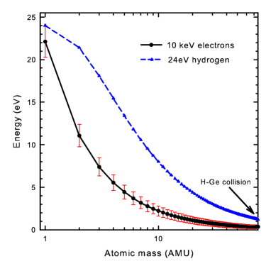
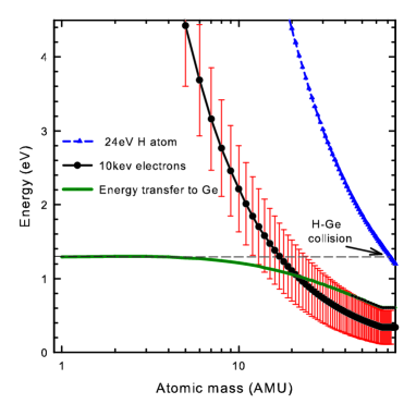
assuming a one dimensional case of an elastic collision where is the initial energy of particle 1. This energy transfer between a 10 keV electron and particles of atomic mass from 1 to 75 is illustrated in Fig. 1 (black solid plot with filled circles). The red bars denote the energy variation if the velocity of the second particle in vacuum is taken into account and including this consideration then the maximum energy transferred to a H atom is approximately 24 eV. Plotting the example of collisions between a 24 eV H atom and particles of atomic mass 1 to 75 illustrates that this knock-on process is capable of transferring the same (only for AMU = 1) or more energy than a direct collision with an electron. To evaluate this process for the specific case of Ge, Figure 2 plots the knock-on energy transfer between particles of various masses that were initially accelerated in a 10 keV electron collision and then collide with a stationary Ge atom. Collisions of the lightest particles with Ge result in the highest energy transfer, that is, at most, eV. This is not sufficient to displace a Ge atom from the lattice but Chen et al ebdefects-Chen1968 noted that defects were only produced in Ge grown in a H atmosphere thus it is likely that H in the crystal lattice played a role. The direct electron-Ge elastic collision process only resulted in eV being transferred to a stationary Ge atom.
b]
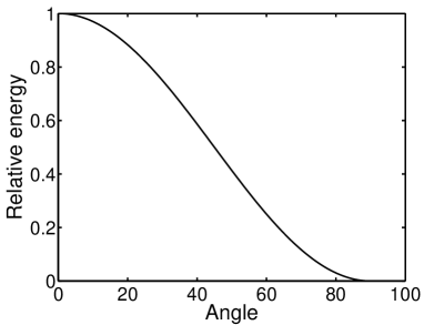
It is also of interest to know how the transfer of energy in collisions depends on the angle. Supposing that a particle of mass and kinetic energy experiences a collision with a particle of mass and this one exits the collision with energy with angle with respect to direction of the incident particle. Then, it is easy to demonstrate that the curve with respect to does not depends on the masses or on the energy of the incident particle as can be seen in Fig. 3. There is a significant interval of exit angles for which is close to the maximum.
3 EBD experimental details
b]
A Ge (111) wafer, bulk grown and doped with Sb to a concentration of cm-3 was degreased in successive 5 minute ultrasonic baths of trichloroethylene, isopropanol and methanol before being etched for 1 minute in a solution of 5:1 H2O:H2O2 (30%). To create an ohmic contact, AuSb was deposited resistively on the wafer back surface and then annealed in an Ar ambient at 350∘C to lower the contact resistance. Samples cut from this wafer were then degreased and etched again before EBD of Pt through a metal contact mask was carried out to yield eight Schottky barrier diodes (SBDs) with a diameter of mm and 50 nm thick on each sample’s front surface. All SBD depositions were carried out using an electron beam with an accelerating voltage of 10 keV and beam current of approximately 100 mA. Current-voltage measurements were carried out on all diodes to verify their suitability for DLTS analysis.
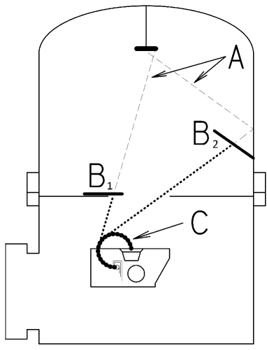
Conditions in the EBD chamber were varied during diode manufacture by a) not applying any counter measures, b) back-filling the chamber with forming gas (H2:N2, 15%:85%) to mbar, c) back-filling with forming gas and placing one shield (B1 in Fig. 4) to shield from direct particles, d) back-filling with forming gas and applying 2 shields (B1 and B2) so that particles reflected off the chamber wall are also shielded for and e) superior vacuum with low H2 concentration as well as both shields in place. The measures taken to ensure that the H2 concentration was maintained below mbar and the DLTS spectra obtained have been published previously ebdefects-Coelho2013 .
To investigate the role of energetic particles arriving at the semiconductor surface during EBD, clean samples were exposed to the conditions of EBD without any evaporation taking place, termed electron beam exposure (EBE) herein, and thereafter Schottky barrier diodes (SBDs) were evaporated resistively onto the irradiated Ge. These samples were exposed for 50 minutes at 100 mA beam current as this was approximately the same amount of exposure that the Pt EBD diodes received. The same measurement procedure was followed as applied previously.
4 Defects after EBD and their origin
The defects introduced during EBD have been reported on before ebdefects-Auret2006 of which the E-center is the most prominent. This defect consists of a vacancy-dopant complex, the dopant in this case being Sb. A control sample manufactured using resistive evaporation RE), a technique known not to introduce defects in Ge, had no measurable defects in it. The peak heights of the DLTS spectra are indicative of defect concentration as
| (4) |
where is the deep level concentration, is the concentration of shallow impurities, is the DLTS peak height and is the junction capacitance. The capacitance of all the devices manufactured was found to be approximately the same and thus spectra can be compared directly.
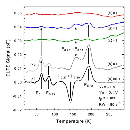
The DLTS spectra in Figs. 5 and 6 were all obtained from diodes prepared in the same EBD system. For spectrum a) a standard oil-filled rotary vane pump was used but for all the other spectra an oil-free pump was used as the fore-pump during deposition. To further improve the vacuum all crucibles were baked out in situ using the electron gun. It is important that the pressure not increase drastically during evaporation although a change in vacuum pressure is inevitable as fixtures heat up during EBD and then outgas. Comparing spectrum a) with spectrum b) it is evident that the peak heights of all the defects that are present in both spectra are reduced by approximately 90% in spectrum b). A further reduction in peak heights can be observed in spectra c), d) and e) once shields were applied. Spectrum e) that represents a diode prepared in a superior vacuum with two shields in place presents as a wavy plot, indicative of surface states, but sharp peaks that are evidence of defects with deep levels are conspicuously absent. Shields B1 and B2 were only capable of blocking off energetic particles that were created when 10 keV beam electrons collide with residual gas atoms or molecules and not for electrons reflected off the evaporant surface. Also, it is expected that light ions will follow a curved trajectory around shield B1 while acted on by the magnetic field of the electron beam thus rendering the shield ineffective to some degree.
The large difference in defect concentration between spectra a) and b) was surprising when one considers that the only difference in the conditions was that less hydrocarbon contamination was present during the manufacture of sample (b) and that the vacuum pressure was kept constant at mbar by introducing forming gas into the chamber. Sample (a) was initially at a vacuum pressure of mbar when the deposition started but this pressure quickly increased to mbar or more as the chamber heated up. The composition of the residual gas present during EBD appears to be the largest contributor to the high defect concentration in sample (a) as well as a higher partial pressure near the electron gun where most of the outgassing occurs. Crucibles used during these evaporations may also have played a role as the standard carbon crucible that was used when preparing sample (a) had a greater impact on the vacuum pressure than the Fabmate® crucible that was used for other samples. The complex nature of conditions present during EBD is evident in Figs 5 and 6 if one considers that the defect concentration increased slightly with the addition of a second shield, a measure designed to lower the defect concentration. This small difference was however not enough to draw conclusions from but most important was that all the counter-measures together lowered the defect density to a level that could no longer be measured. For a diode evaporated onto Si the same measures lowered the defect density so that, although the DLTS peaks were small, some defects could still be identified ebdefects-Auret2012 .
The maximum energy that can be transferred by impinging atoms to the Ge lattice per collision can be read off graph 2 (thick green plot). Treating all collisions elastically is a reasonable simplification to obtain the maximum possible energy that can be transferred whereas treating the electrons relativistically only served to increase the energy transferred by % and need not be taken into account. The maximum energy that can be transferred to Ge was found to be approximately eV via a light atom like H, with maximum energy transferred decreasing as the intermediate atom or particle increases in mass. This energy is not sufficient to dislodge a Ge atom from its position in the crystal lattice but may dislodge a light atom that has taken up a substitutional position in the lattice or modify an existing defect with an energy level too close to the band edges to be detected using DLTS. Vacancy-hydrogen complexes have been reported on previously in Ge ebdefects-Coomer1999 and were observed using infrared spectroscopy ebdefects-Budde1999 . There is at present no certainty which of these complexes plays a role in defect formation during EBD as their concentration in bulk grown Ge is too low to be detected with infrared spectroscopy.
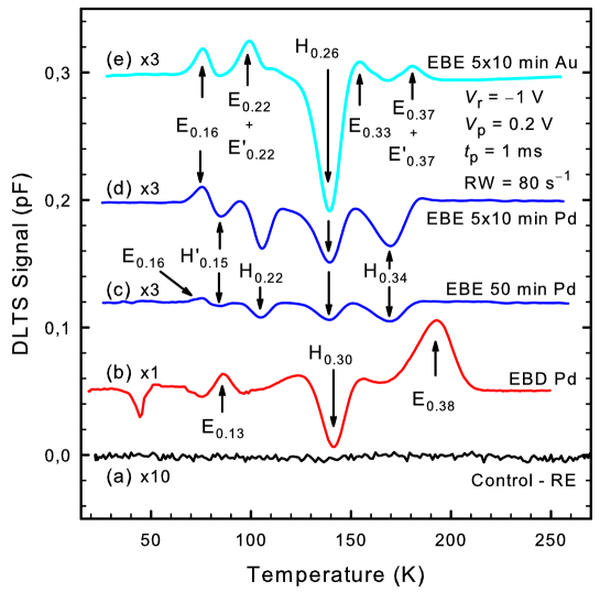
The defects that were observed after electron beam exposure of Ge that numbered ten different defects, in total, have not been observed before with the exception of E0.37 and E0.38 (E-center). The defect concentration of EBE induced defects was much lower than that measured after EBD for similar exposure times and this is evident if one compares plots b) and c) of Fig. 6. During EBD the semiconductor receives a measure of protection from impinging particles as it is exposed to radiation through an ever increasing metal film. No such layer is present during EBE thus it was expected that similar or more damage would be observed after the EBE process. One possibility for the great variety of different defects observed is that these defects are mostly due to atoms being implanted into the EBE treated Ge but this cannot explain the absence of the EBD induced defects. That the metal layer acts as a channel for energy to be transferred to the semiconductor is a possibility that will require further investigation. Samples exposed for 50 minutes in 10 minute increments interrupted with 50 minute periods to allow for cooling exhibited significantly higher defect concentrations for all defects observed. The sample that was subjected to a continuous 50 minute EBE heated up 35∘C more than the sample that was allowed to cool. Differences in defect concentrations may be due to annealing, in part, but cannot explain why all the EBE induced defects were equally affected. The other possibility is that sample heating interrupts the energy transfer process leading to less defects being introduced. Detailed annealing studies will be required to shed more light on this result.
5 Intrinsic localized modes and defects
For many years the paradigm of considering phonons as the entity transporting energy in a solid has been overwhelming. Phonons as it is well known are obtained under the hypothesis of small lattice vibration that allows the linearization of the dynamical equations of the system or equivalently allows the use of the harmonic approximation for potentials. Perhaps one of the clearest example of success was Einstein solid theory where phonons were quantized in Ref. ebdefects-Einstein1906 at the beginning of XXth century. Linear systems and phonons have been extremely successful not only in the framework of quantum mechanics but also classical mechanics linear lattice theory has been very productive. Most of the theory of spectroscopy is based on the harmonic approximations and phonons.
5.1 Limitations of harmonicity
It is however based on several assumptions that are known to be convenient mathematical tools but not accurate representations of reality. First, it is well known that interatomic potentials are not harmonic, starting from the electrostatic interaction and continuing from Van der Waals forces described for example with Buckingham potentials . However, the harmonic approximation is quite convenient at temperatures of the order of room temperature and above, for which the average atomic displacement are not too large. The key word is average, for average displacements or properties. At any temperature there is a small but finite probability that some displacements are large enough for the harmonic approximation to become invalid, but they will have a small effect in the average properties. However, even if considering only bulk properties, it is well known that the harmonic approximation is not sufficiently accurate as such a solid would not experience thermal expansion and would have an infinite thermal conductivity ebdefects-ashcroft1976 .
There is a huge change, when interaction with radiation or swift particles is considered. In this article, for example, we considered the possible interaction of very low energy particles such as 10 keV electrons or 24 eV H atoms. Germanium atoms may acquire energies of 1 eV, forty times larger than the average thermal energy at room temperature. For the displacements involved we can be sure that nonlinear effects will take place. If the interatomic distances become small enough, potentials with a strong repulsive core such as Lennard-Jones or Ziegler-Biersack-Littmark (ZBL) ebdefects-ziegler1980 ; ebdefects-ziegler2008 need to be introduced to provide a realistic description of the forces. If the energies are large enough they will produce defects in the solid by displacing atoms from their lattice positions, bringing about the formation of point defects like interstitials or vacancies. In this article and in this section we will focus our attention in energies that are not large enough to disrupt the lattice geometry, the so called subthreshold radiation regime. The threshold energy in Ge depends on the lattice direction, being 11.5 eV and 19.5 eV for the and directions, respectively ebdefects-holmstrom2010 . Conventional knowledge supposes that the energy just disperses into phonons elevating locally the temperature of the sample creating a thermal spike but which soon would relax to thermal equilibrium with the rest of the crystal.
Another shortcoming of the phonon description is that phonons are harmonic waves that extend over the whole space. This is a very useful mathematical hypothesis and it is justified because the extension of the phonons is much larger than the lattice unit. However, the impact of a 10 keV electron or a 24 eV H atom on Ge is clearly a localized phenomenon, because the de Broglie wavelength is nm, smaller than an atom size. In the harmonic approximation the consequence of such an impact is a wave packet but because basically all media are dispersive it soon disperses into phonons with different wavelengths and velocities and the localization is lost.
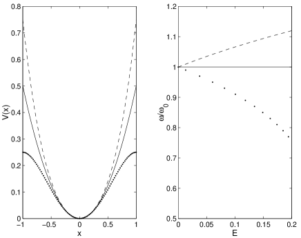
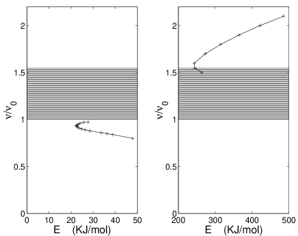
However, if the nonharmonicity of the potentials is taken into account such an impact may produce what is called an intrinsic localized mode (ILM), also known as a breather, depending on the context ebdefects-Kosevich1974 ; ebdefects-sieverstakeno88 ; ebdefects-james04 ; ebdefects-MA94 . This is a localized wave packet that does not spread, that is, it behaves like a quasiparticle. As ILMs are not exact solutions they will eventually lose energy and disperse into phonons. How long they can live, how many of them are there and how important they are, are still open questions that are very much related and that we address here briefly. The key concept to understand breather existence is the fact that the frequency of vibration of nonlinear oscillators depends on the amplitude or energy of them, which does not happen in a linear oscillator. If the frequency of the oscillator increases with the amplitude, it is called a hard potential. This corresponds to a potential that grows faster with the distance to the equilibrium point than what the harmonic one does, while being equal at small distances. If the frequency of the oscillator decreases with energy, it is called a soft potential and it grows more slowly than the harmonic one does, as is illustrated in Fig. 7. The phonon spectrum of a solid is always bounded from above, may have gaps, and in some cases may also be bounded from below, in which it is called optical. If it is not bounded from below it is called acoustic. Vibrations with frequencies that are outside the phonon spectrum cannot propagate in the solid, bringing about localization of energy that does not spread. Figure 8 shows an example for a model of cations in a silicate layer which produces the optical spectrum ebdefects-archilla2008 .
Breathers are well described mathematical objects and are easy to produce in macro and meso systems. For example, a chain of magnetic pendulums is easy to construct and to experiment with ebdefects-russellzolotaryuk97 . Their existence in a solid is a more difficult question for several reasons, to cite a few: a) the reality is quantum and not classical; b) the potentials are simplifications of complex interactions; c) the lattice is not perfect; d) the lattice is disordered due to temperature. These subjects have been studied, theories of quantum breathers exist and molecular dynamics using increasingly realistic and complex potentials have been useful in creating ILMs of energies of the order of magnitude of eV ebdefects-voulgarakis2004 ; ebdefects-haas2011 ; ebdefects-hizhnyakov2014 that propagate at finite temperatures. But more importantly, there is growing experimental evidence of long range localized transmission of energy. For example, it was observed ebdefects-russelleilbeck2011 that subsequent to the impact of an alpha particle on the surface of an insulator, there was transmission of energy in a localized way along close packed lines that was able to eject an atom at the surface of the crystal. For the material of interest in this article, germanium, it was shown that the impact of Ar atoms of 2-8 eV were able to anneal defects 2 m below the surface ebdefects-archilla-coelho2015 ; ebdefects-archillacoelhoquodons2015 . Annealing and ordering of voids in several crystals attributed to ILMs ebdefects-dubinkoguglya2011 is just another example.
5.2 Effect of intrinsic localized modes
One question is if ILM do exist in a solid, what will be the effect and on which properties. If there are many of them they will probably interact between them and will be dispersed. The main effect will be an increase of the temperature of the system, similarly for a harmonic lattice. It seems that one of the most important effects of breathers could appear in connection with changes of structure, annealing, chemical reactions and similar processes. Generally speaking all processes for which a potential barrier with some activation energy has to be overcome and with a probability of happening proportional to , that is, the constant rate of the process is given by an Arrhenius type equation:
| (5) |
This equation is extremely sensitive to changes in and it is also asymmetric, i.e., the increase in the rate corresponding to a decrease of energy is much larger than the decrease in the rate corresponding to an increase of the same amount of energy. An easy calculation shows it. Suppose that there is some perturbation of the barrier during some time and a perturbation during the same time, then, the mean rate during the time interval would be:
| (6) | |||||
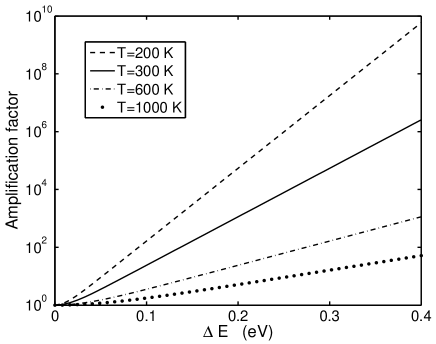
The amplification factor is and can usually be approximated by . It does not depend on the height of the barrier but only on the ratio of the barrier variation and the thermal energy of the lattice. It can be seen in Fig. 9. An elaborate and rigorous theory is developed in Refs. ebdefects-dubinko2011 ; ebdefects-dubinko2013 ; ebdefects-dubinkoarchillaquodons2015 , but the conclusions are the same. Therefore, ILMs of small energy, both mobile or stationary can produce a huge effect. Even more if we consider that their energy is localized and not extended as for phonons.
An example of this phenomenon in a silicate is described in Ref. ebdefects-ACANT06 . In an experiment, reconstructive transformation of the mica muscovite into lutetium disilicate was observed to occur several orders of magnitude faster than expected due to the nature of the bonds that have to be broken. The explanation is based on a fact observed in numerical simulations: that breathers with larger energy live longer, therefore a temporary fluctuation that produces an accumulation of vibrational energy and creates an ILM is not immediately destroyed ebdefects-piazza03 . The more energetic the ILM the more unlikely, but also the longer the lifetime. Eventually an equilibrium between ILM creation and destruction is achieved for each energy. This is a very low population with no thermodynamical effects but with larger mean energy than phonons. This energy is also localized and can be delivered more effectively to the bonds that are to be broken. Another example for germanium consists of a series of experiments where it was found that Ar plasma ions with energies of 2-8 eV were able to anneal defects like the E-center at least two m below the surface ebdefects-archilla-coelho2015 . On the other hand EBD was found to create defects up to a depth of one m ebdefects-Coelho2013 .
6 Conclusions
It was established that during EBD energetic particles, the product of elastic collisions between 10 keV electrons and residual gas atoms in the vacuum, were the primary cause of defects introduced in Ge and Si. High energy electrons interacting with the semiconductor directly were found to transfer far less energy, per collision, than if the energy transfer occurred through an intermediary atom or molecule. The maximum energy transferred via this two-step process was calculated to be approximately eV for particles with an atomic mass from 1 to 4 and then diminished for heavier particles. This amount of energy, when transferred to a Ge lattice atom, is incapable of creating a Frenkel pair but may be sufficient to modify an existing defect structure that was previously invisible to DLTS. This conclusion can also be drawn if n-Si is used ebdefects-Auret2012 . The energies transferred to the germanium lattice by EDB is typically of the order of magnitude of intrinsic localized modes. These nonlinear localized wave packets have the property of significantly increasing the probability of structure changes by temporally lowering the potential barrier for the process. Therefore, intrinsically localized modes are very likely to be the cause of the observed phenomenon
Samples exposed to the conditions of EBD, without deposition (termed EB exposure) did not contain the same defects as the EBD samples except for E0.37 and the vacancy-antimony center (V-Sb), E0.38. This implies that a necessary condition for the introduction of EBD defects was a thin metal layer through which energy was transferred to the germanium crystal lattice. The EB exposure defects have not yet been identified and may be related to impurities that were accelerated into the germanium near-surface region before diffusing deeper into the material, although this cannot explain the low defect concentrations observed, especially if the sample temperature was allowed to increase during treatment.
Acknowledgments
This project has been financed by the South African National Research Foundation. J.F.R.A. acknowledges financial support from the project FIS2008-04848 from Ministerio de Ciencia e Innovación (MICINN).
References
- (1) Archilla, J.F.R., Coelho, S.M.M., Auret, F.D., Dubinko, V.I., Hizhnyakov, V.: Long range annealing of defects in germanium by low energy plasma ions. Physica D 297, 56–61 (2015)
- (2) Archilla, J.F.R., Coelho, S.M.M., Auret, F.D., Nyamhere, C., Dubinko, V.I., Hizhnyakov, V.: Experimental observation of moving intrinsic localized modes in germanium. In: J.F.R. Archilla, N. Jiménez, V.J. Sánchez-Morcillo, L.M. García-Raffi (eds.) Quodons in mica: nonlinear localized travelling excitations in crystals. Springer (2015). To appear
- (3) Archilla, J.F.R., Cuevas, J., Alba, M.D., Naranjo, M., Trillo, J.M.: Discrete breathers for understanding reconstructive mineral processes at low temperatures. J. Phys. Chem. B 110(47), 24,112–24,120 (2006)
- (4) Archilla, J.F.R., Cuevas, J., Romero, F.R.: Effect of breather existence on reconstructive transformations in mica muscovite. AIP Conf. Proc. 982(1), 788–791 (2008)
- (5) Ashcroft, N.W., Mermin, N.D.: Solid State physics. Saunders College Publishing, Philadelphia (1976)
- (6) Aukerman, L.W.: Radiation effects. In: Physics of III-V compounds, V. 4, Semiconductors and Semimetals, pp. 343–409. Elsevier (1968)
- (7) Auret, F.D., Coelho, S.M.M., Nel, J.M., Meyer, W.E.: Electrical characterization of defects introduced in n-Si during electron beam deposition of Pt. Physica Status Solidi A 209(10), 1926–1933 (2012)
- (8) Auret, F.D., Meyer, W.E., Coelho, S.M.M., Hayes, M.: Electrical characterization of defects introduced during electron beam deposition of Pd schottky contacts on n-type Ge. Appl. Phys. Lett. 88(24), 242,110–4 (2006)
- (9) Auret, F.D., Mooney, P.M.: Deep levels introduced during electron-beam deposition of metals on n-type silicon. J. Appl. Phys. 55(4), 988–993 (1984)
- (10) Bauer, W., Sosin, A.: Threshold displacement energies and subthreshold displacements in copper and gold near k. J. Appl. Phys. 35(3), 703–709 (1964)
- (11) Budde, M., Bech Nielsen, B., Keay, J.C., Feldman, L.C.: Vacancy hydrogen complexes in group-IV semiconductors. Physica B 273-274, 208–211 (1999)
- (12) Chen, Y., MacKay, J.W.: Subthreshold electron damage in n-type germanium. Phys. Rev. 167(3), 745–753 (1968)
- (13) Coelho, S.M.M., Auret, F.D., Janse van Rensburg, P.J., Nel, J.: Electrical characterization of defects introduced in n-Ge during electron beam deposition or exposure. J. Appl. Phys. 114(17), 173,708 (2013)
- (14) Coomer, B.J., Leary, P., Budde, M., Bech Nielsen, B., Jones, R., Öberg, S., Briddon, P.: Vacancy-hydrogen complexes in germanium. Mater. Sci. Eng. B 58(1-2), 36–38 (1999)
- (15) Corbett, J.W., Bourgoin, J.C.: Defect creation in semiconductors. In: J.H. Crawford Jr., L.M. Slifkin (eds.) Point Defects in Solids, vol. 2, Semiconductors and Molecular Crystals, pp. 1–161. Springer, New York (1975)
- (16) Dobaczewski, L., Kaczor, P., Hawkins, I.D., Peaker, A.R.: Laplace transform deep-level transient spectroscopic studies of defects in semiconductors. J. Appl. Phys. 76(1), 194–198 (1994)
- (17) Dubinko, V.I., Archilla, J.F.R., Dmitriev, S.V., Hizhnyakov, V.: Rate theory of acceleration of defect annealing driven by discrete breathers. In: J.F.R. Archilla, N. Jiménez, V.J. Sánchez-Morcillo, L.M. García-Raffi (eds.) Quodons in mica: nonlinear localized travelling excitations in crystals. Springer (2015). To appear
- (18) Dubinko, V.I., Dubinko, A.V.: Modification of reaction rates under irradiation of crystalline solids: contribution from intrinsic localized modes. Nucl. Instrum. Meth. B 303, 133–135 (2013)
- (19) Dubinko, V.I., Guglya, A.G., Donnelly, S.E.: Radiation-induced formation, annealing and ordering of voids in crystals: Theory and experiment. Nucl. Instrum. Meth. B 269(14), 1634–1639 (2011)
- (20) Dubinko, V.I., Selyshchev, P.A., Archilla, J.F.R.: Reaction-rate theory with account of the crystal anharmonicity. Phys. Rev. E 83, 041,124 (2011)
- (21) Einstein, A.: The Planck theory of radiation and the theory of specific heat. Ann. Phys. 22(1), 180–190 (1906)
- (22) Graper, E.B.: Electron beam evaporation. In: D. Glocker, S. Shah (eds.) Handbook of Thin Film Process Technology, chap. A1.2. Taylor & Francis, Bristol, UK and Philadelphia, USA (1996)
- (23) Hass, M., Hizhnyakov, V., Shelkan, A., Klopov, M., Sievers, A.J.: Prediction of high-frequency intrinsic localised modes in Ni and Nb. Phys. Rev. B 84, 144,303 (2011)
- (24) Hizhnyakov, V., Haas, M., Shelkan, A., Klopov, M.: Theory and md simulations of intrinsic localized modes and defect formation in solids. Phys. Scr. 89(4), 044,003 (2014)
- (25) Holmström, E., Nordlund, K., Kuronen, A.: Threshold defect production in germanium determined by density functional theory molecular dynamics simulations. Phys. Scr. 81, 035,601 (2010)
- (26) Karazhanov, S.Z.: Mechanisms for the anomalous dependence of carrier lifetime on injection level and photoconductance on light intensity. J. Appl. Phys. 89(1), 332–335 (2001)
- (27) Kleinhenz, R., Mooney, P.M., Schneider, C.P., Paz, O.: Defects produced in silicon and GaAs during E-beam evaporation of metals. J. Electron. Mater. 14a, 627–633 (1985)
- (28) Klose, H.A., Thiele, P., Zinnow, S.: Modification of near-surface regions in Si by low energy particles. Surf. Coat. Technol. 59(1-3), 221 – 225 (1993)
- (29) Kosevich, A.M., Kovalev, A.S.: Self-localization of vibrations in a one-dimensional anharmonic chain. Sov. Phys. JETP 40(5), 891–896 (1974)
- (30) Lang, D.V.: Deep-level transient spectroscopy: A new method to characterize traps in semiconductors. J. Appl. Phys. 45(7), 3023–3032 (1974)
- (31) van Lint, V., Flanagan, T., Leadon, R., Naber, J.: Mechanisms of radiation effects in electronic materials, vol. 1. Wiley-Interscience (1980)
- (32) MacKay, R.S., Aubry, S.: Proof of existence of breathers for time-reversible or Hamiltonian networks of weakly coupled oscillators. Nonlinearity 7, 1623 (1994)
- (33) Naber, J.A., James, H.M.: Effect of hydrogen on the displacement process in Ge. Bull. Am. Phys. Soc. 2(6), 303 (1961)
- (34) Piazza, F., Lepri, S., Livi, R.: Cooling nonlinear lattices toward energy localization. Chaos 13(2), 637–645 (2003)
- (35) Reinhold, E., Faber, J.: Large area electron beam physical vapor deposition (EB-PVD) and plasma activated electron beam (EB) evaporation - Status and prospects. Surf. Coat. Technol. 206(7), 1653–1659 (2011)
- (36) Russell, F.M., Eilbeck, J.C.: Persistent mobile lattice excitations in a crystalline insulator. Discret. Contin. Dyn. S.-S 4, 1267–1285 (2011)
- (37) Russell, F.M., Zolotaryuk, Y., Eilbeck, J.C., Dauxois, T.: Moving breathers in a chain of magnetic pendulums. Phys. Rev. B 55, 6304 (1997)
- (38) Sánchez-Rey, B., James, G., Cuevas, J., Archilla, J.F.R.: Bright and dark breathers in Fermi-Pasta-Ulam lattices. Phys. Rev. B 70, 014,301–1–014,301–10 (2004)
- (39) Sievers, A.J., Takeno, S.: Intrinsic localized modes in anharmonic crystals. Phys. Rev. Lett. 61, 970–973 (1988)
- (40) Voulgarakis, N.K., Hadjisavvas, S., Kelires, P.C., Tsironis, G.P.: Computational investigation of intrinsic localization in crystalline Si. Phys. Rev. B 69, 113,201(1–4) (2004)
- (41) Ziegler, J.F., Biersack, J.P., Littmark, U.: In The Stopping and Range of Ions in Matter, vol. 1. Pergamon, New York (1985)
- (42) Ziegler, J.F., Biersack, J.P., Ziegler, M.D.: SRIM - The Stopping and Range of Ions in Matter. Published by James Ziegler, Chester, Maryland (2008)