Observation of geometry dependent conductivity in two-dimensional electron systems
Abstract
We report electrical conductivity measurements on a range of two-dimensional electron gases (2DEGs) of varying linear extent. Intriguingly, at low temperatures () and low carrier density () we find the behavior to be consistent with , where is the length of the 2DEG along the direction of transport. Importantly, such scale-dependent behavior is precisely in accordance with the scaling hypothesis of localization [Abrahams et al., Phys. Rev. Lett. 42, 673 (1979)] which dictates that in systems where the electronic wave function is localized, is not a material-specific parameter, but depends on the system dimensions. From our data we are able to construct the ”-function” and show this to be strongly consistent with theoretically predicted limiting values. These results suggest, remarkably, that the electrons in the studied 2DEGs preserve phase coherence over lengths m. This suggests the utility of the 2DEGs studied towards applications in quantum information as well as towards fundamental investigations into many-body localized phases.
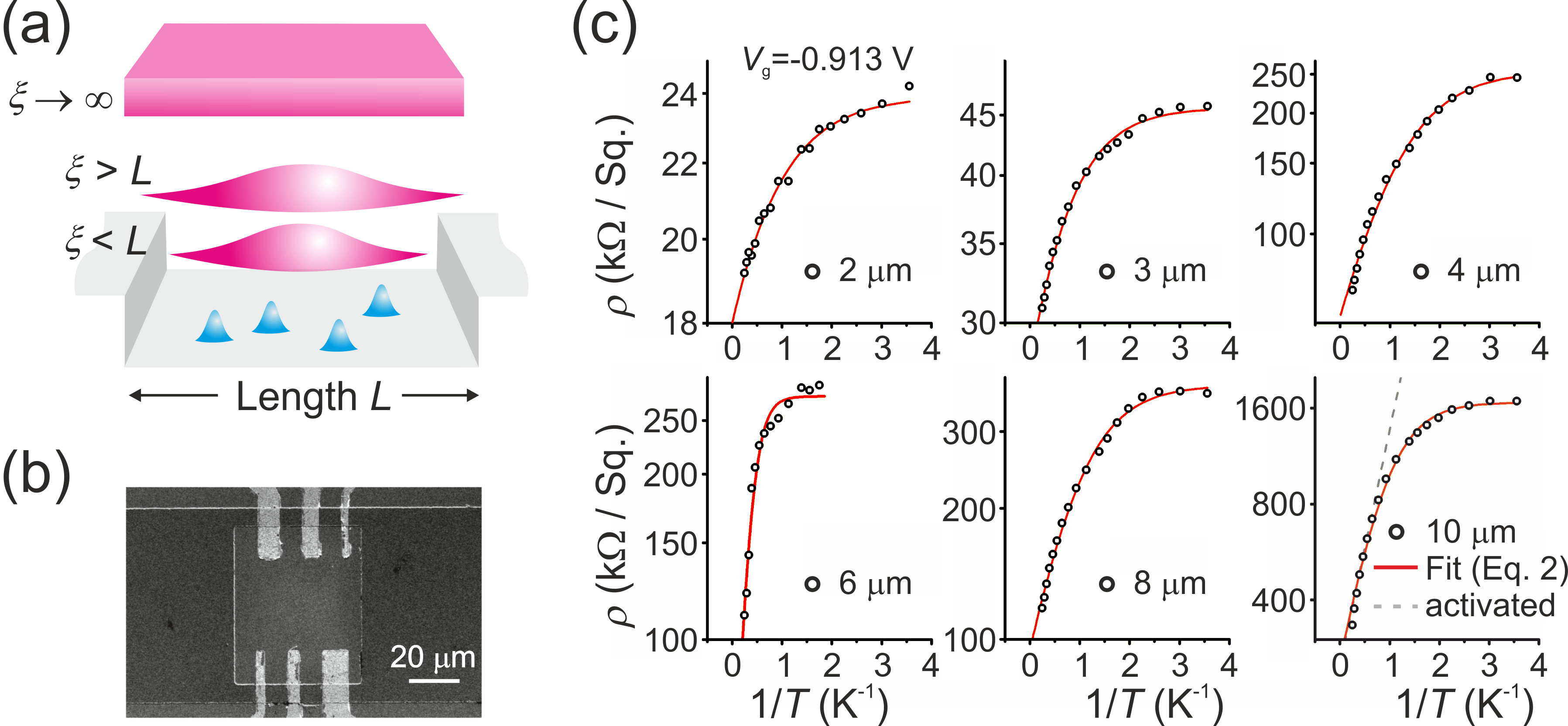
The scaling hypothesis of localization AALR , formulated over thirty years ago, is a statement that the electrical conductivity is lengthscale-dependent in finite systems where the conduction electrons are short-ranged or localized. This can be understood by considering electronic states with localization length in systems of different spatial extents: As depicted in Fig. 1(a), if is greater than the linear extent of the system, then electrons are able to communicate across the system ends and there will be a finite conductance even at K. However, this conductance will decrease as the system size increases, ultimately vanishing for infinitely large systems. On the other hand, if the electronic states are extended, , then even in the infinite system-size limit, . This intuitive picture is at the very heart of the scaling hypothesis which distinguishes between metallic and insulating states on the basis of the range of : If the electronic states at the chemical potential are extended, then the system is a metal, but if they have a finite extent, the system is an insulator. In other words, the metallic state is defined by independent of system dimensions, whereas the insulating state is characterized by decaying with increasing system dimensions. This underlies the Anderson metal-to-insulator transition in which a ”mobility-edge” in wave vector -space demarcates short-ranged and long-ranged states EversMirlinRMP2008 .
However, since the scaling hypothesis was put forward, to our knowledge there have been no experimental reports of length-dependent . In this paper, working with mesoscopic GaAs-based 2DEGs of varying linear extent , we provide the experimental demonstration of -scaling consistent with the scaling hypothesis. We continuously tune in the 2DEGs by applying a top-gate voltage and observe a crossover from a regime in which the electrical resistivity is independent of to one where it is strongly dependent on . We find our results to be strongly consistent with the scaling predictions AALR .
In low-disorder two-dimensional (2D) systems , where is the electronic mean free path and is the Fermi wave vector. Using a 2DEG equipped with a top-gate electrode allows one to tune the carrier density and thereby . Furthermore, since governs the degree to which any charged scattering centers are screened, this process also serves to vary which, in turn, can be estimated from the measured SM . Clearly, when , can be macroscopically large, and this results in what is known as the ”weakly localized” (WL) phase of electrons. The WL phase displays many outwardly metallic characteristics AbrahamsRMP2001 ; Simmons_etal_PRL2000 ; Hamilton_etal_PRL2001 ; Uren_etal_JPhysC1981 including to the lowest achievable Kravchenko_PRB1995 ; LiPRL2003 ; PudalovPRL2003 , the hallmark of metallic conduction. When experiments observe an abrupt crossover to the ‘strongly’ or ‘Anderson’ localized (AL) phase in which , the effective Bohr radius in GaAs-based 2DEGs nm. In this regime is completely suppressed, although at finite conduction occurs through phonon-assisted ‘hops’. This gives rise to , where is the hopping energy, is the Boltzmann constant and 1, 1/2 or 1/3 depending on whether the hopping is nearest-neighbour hopping MottDavis , hopping in the presence of the Coulomb gap ES_JPhysC1975 , or variable-range hopping MottDavis , respectively. In other words, the sign of can serve as a diagnostic to distinguish between metallic and insulating states. However, as we will directly show in this paper, the -dependence alone is an insufficient test of metallicity. This is because, even in situations where , (i.e., the system is, by definition, an insulator) can be negative if .
Experiments so far are consistent with the two limiting instances of (WL) and (AL), neither of which, importantly, are expected to show -scaling. This is obvious in the AL or ”hopping” regime since phonons, which mediate the hopping transport, exist homogeneously in space. The reasons for the absence of scaling behavior in the WL regime are, however, more subtle and perhaps linked to the macroscopic samples employed. Localization arises due to interference of the electronic wave function and thus relies crucially on phase coherence. The phase coherence length is defined as the length over which the phase of the electron is completely randomized through inelastic interactions. Therefore scaling behavior is only expected when , a condition which may not have been rigorously met in earlier experiments DaviesPepperKavehJPhysC1983 .
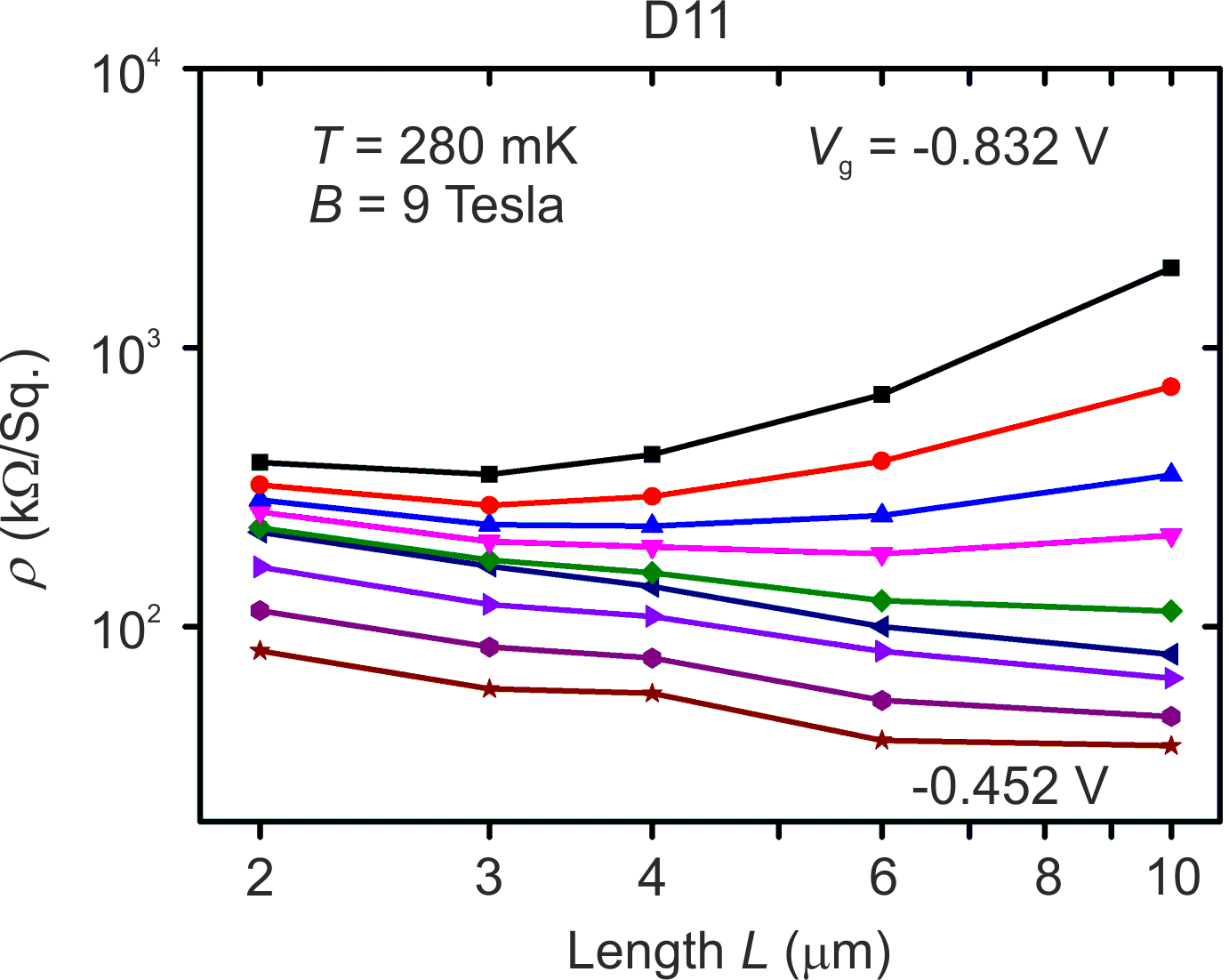
Here we perform a systematic size-dependence study of 2DEGs with varying and width . As shown in Fig. 1(b), our devices each contain six top-gate-defined 2DEGs with constant width and length ranging from 2 to 10 m. We have fabricated devices with 3 m (D3), 9 m (D9), and 11 m (D11), and here we focus on the results from D9 and D11. Please refer to the Supplemental Material SM for details of the wafers used, device fabrication and measurement setup.
Figure 1(c) shows resistivity against for the six 2DEGs in D9 at gate voltage V. Here is evaluated as , where is measured in a quasi-four-terminal setup SM . The corresponding values are all and SM with determined from Drude theory. This would normally be the strongly localized regime where the dependence for an insulator can be expected. Remarkably, for K, indicating the presence of metallic states as defined above GhoshPRB2004 ; BaenningerPRL ; KoushikPRB ; NarayanPRB ; NarayanJLTP . While the device geometry has very little influence on the value of at which metallic conduction sets in, it is noteworthy that the value is strongly device-dependent. This is despite the fact that the data are at the same value of , that the 2DEGs are located close to each other on the host wafer, and that they are all cooled down simultaneously under the same conditions. Importantly, while this behavior stands in stark contrast to the commonly observed 2D “metal-to-insulator” transition, it suggests that the insulating and metallic states might be intimately linked.
| (K) | |||
|---|---|---|---|
| 9x10 | 2.250.08 | 273.8714.41 | 171318.94 |
| 9x8 | 1.680.06 | 114.224.14 | 409.514.93 |
| 9x6 | 6.490.39 | 43.794.66 | 281.225.20 |
| 9x4 | 1.500.04 | 78.002.26 | 260.923.04 |
| 9x3 | 1.640.06 | 63.211.37 | 45.140.22 |
| 9x2 | 0.970.04 | 74.091.12 | 24.760.12 |
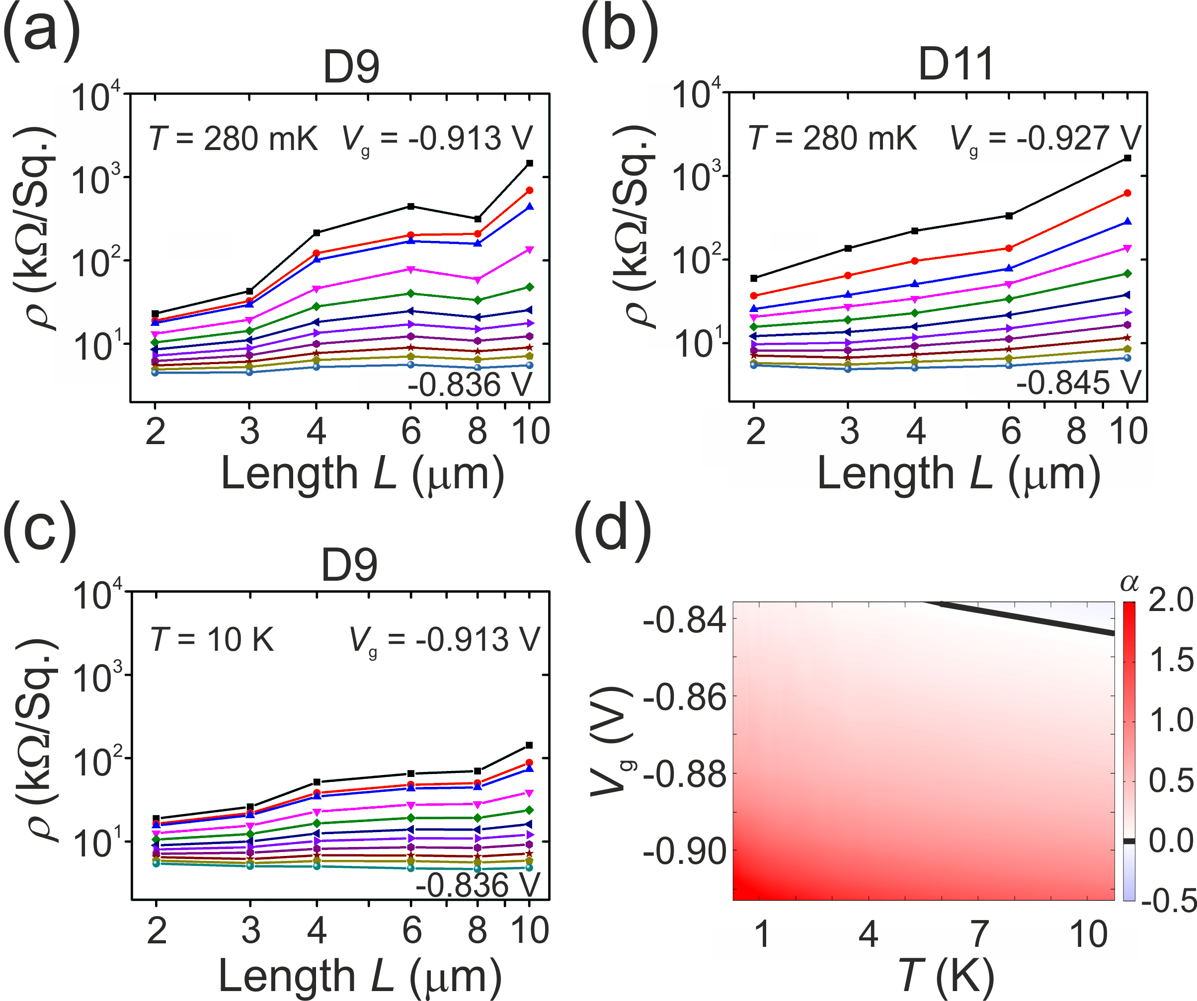
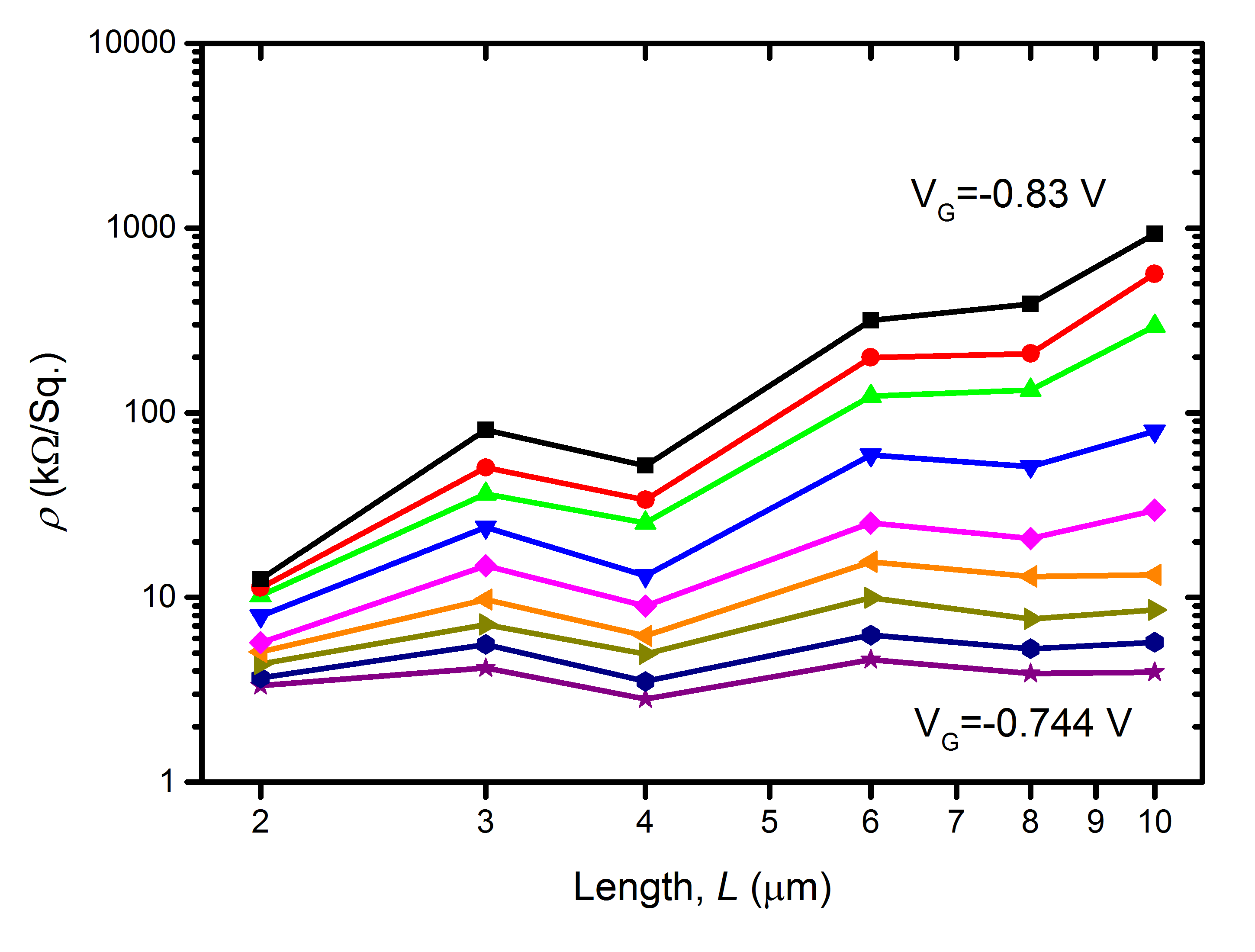
Figures 2(a) and 2(b) show as a function of at K for D9 and D11, respectively. Interestingly, we find that the dependence seems broadly consistent with . The exponent decreases as increases and, as shown in Fig. 2d, goes to zero at a -dependent . We emphasize that the data shows the resistivity and not resistance, and thus any geometry-dependent characteristics are very unexpected. Figure 2(c) shows at 10 K, and remarkably, we still find a clear and systematic dependence in . It even appears that at the lowest there is a slight negative slope [also seen in the top-right corner in Fig. 2(d)], but this is a measurement artifact that becomes important only at low (see Ref. SM ).
In all our measurements, we came across only one 2DEG (D11, = 8 m) in which deviated by more than 10% from .
In the following, we analyze our experimental findings in light of the scaling hypothesis which states that
| (1) |
Here the first term on the right is the conductivity at a microscopic length scale , and the second term is the size-dependent reduction in arising due to the exponentially decaying envelope of . The microscopic length scale is the smaller of and . We assume that is sufficiently low such that , an assumption which we will reexamine later. Therefore the first term is identically equal to the Drude conductivity SM , where is the electron charge, is the momentum scattering time, and is the electron effective mass in GaAs = 0.067, with being the bare electron mass. It is therefore important to note that only when = 1 and is suppressed for larger . The length scale over which is , and this provides an estimate for . On intermediate length scales, Eq. (1) clearly indicates that (incorrectly) identifying as results in an underestimate for and, importantly, that . Indeed, as shown in Fig. 3(a), upon fitting the measured to Eq. (1), we obtain 100 nm at the lowest accessible , which is significantly greater than the nominally obtained values. We are able to map from to by tuning the device to the quantum Hall regime and observing edge-state reflections as is decreased BaenningerPRB2005 and thereby ascertain that the corresponding = 1.4 1014 m-2. This results in 3, even though the measured is orders of magnitude greater than and (see Fig. 2). For , we estimate 11 m which, crucially, is comparable to the device dimensions. Similar results are obtained for D11, and is plotted as a function of in Fig. 3(b).
Figs. 3(c) and 3(d) provide a complementary look at the scaling behavior in our data by examining the scaling function as a function of , where . is evaluated from each pair of neighboring points in Figs. 2(a) and 2(b). The general trend in (solid red line) agrees well with the theoretical limits of for very large and small . These theoretical limits arise from a combination of dimensional considerations in the low-disorder () regime and some basic assumptions about the overlap of localized states in the high-disorder () regime. In the former, where disorder and scattering are weak, the electronic wave function will have a very large extent, and it is reasonable to expect that is intensive , where d is the dimensionality of the system under study. In the latter, where disorder is strong and the electronic wave function is localized, conduction is governed by the spatial overlap of neighboring states. However, such localized states cannot cumulatively result in an extended state since states in close spatial proximity are necessarily widely separated in energy. Thus is exponentially suppressed , independent of dimensionality. These expressions for provide the theoretically expected limits in , which in 2D reduce to for and for . We find the averaged , obtained from our measurements, exactly in the range in between the theoretically expected limiting values. It is noteworthy that Fig. 3 provides evidence of finite within the WL regime where where the subscript denotes ”scaling theory”.
Thus the picture emerges that the 2DEGs studied are, in fact, in the weakly localized regime but with significantly reduced due to the finite extent of . Therefore, the weak dependence and even positive slope of against are entirely expected. The question then arises as to why above 1 K the 2DEGs show activated transport. The point here is that the metallic character below 1 K is imparted by the relatively long electronic states at , but states with , which nominally do not contribute to transport due to phase space restrictions, are continually hopping due to inelastic interactions with phonons. These therefore provide an additional transport channel with an activated form. We thus propose a simple ”parallel-resistor” model to understand the -dependence of in which the conducting states (at ) and hopping states (at ) conduct in parallel:
| (2) |
Here is the contribution due to the effectively extended states assumed to be independent, and the second term on the right is the hopping term. As shown in Fig. 1(c), we are able to obtain excellent fits to the data using , and as fitting parameters. Values of the resulting fit parameters are listed in Table 1. A noteworthy, though small, feature that the model does not capture is the mildly positive seen at 2 K-1 in the lower-middle panel of Fig. 1(c) (see also Ref. BaenningerPRL ). However, this is trivially so due to the assumption of constant which disregards effects such as electron screening DasSarmaHwang_PRL1999 and interelectron interactions Zala_etal_PRB2001 , including which will, no doubt, result in more accurate models.
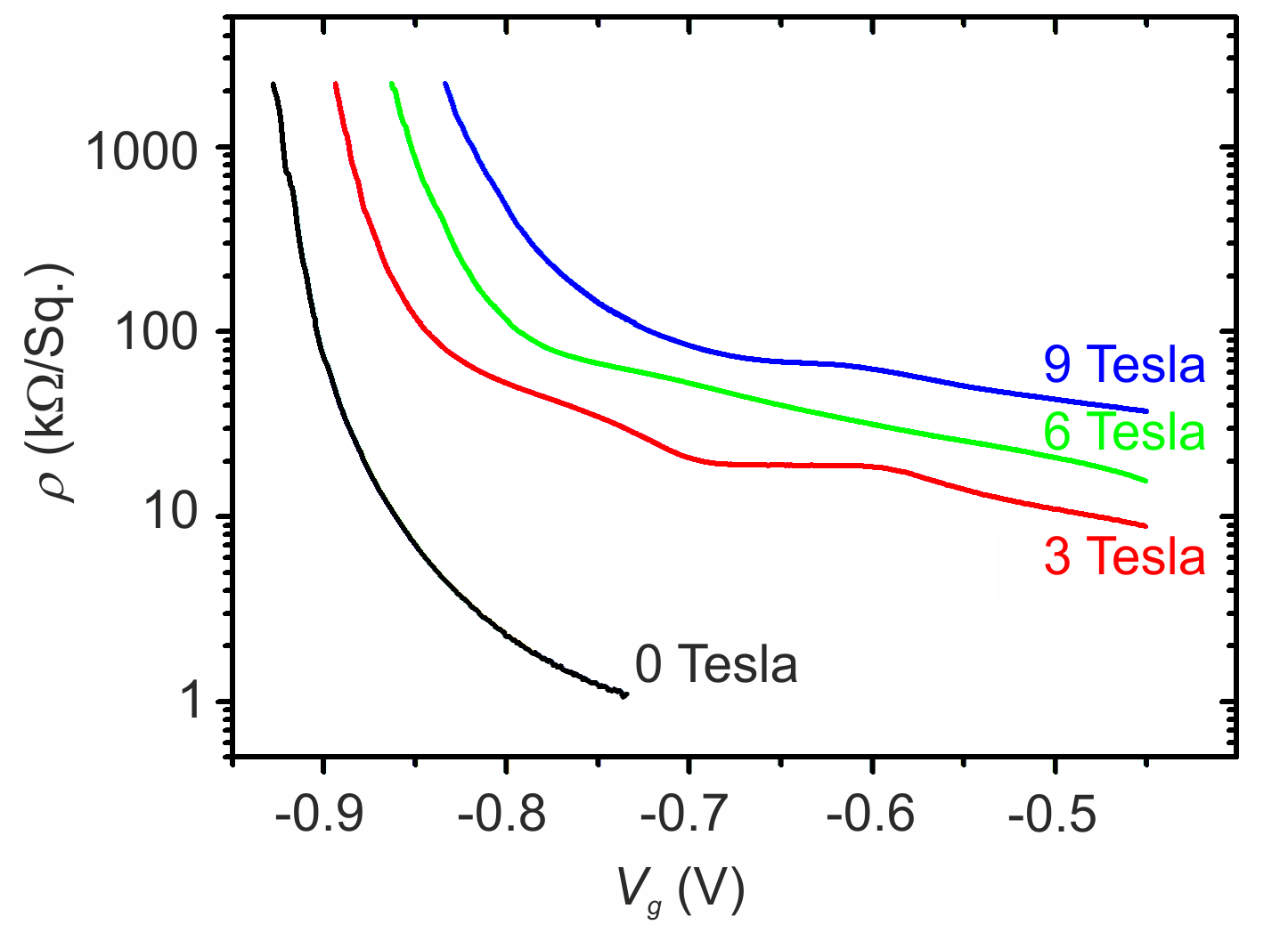
We now return to our assumption that , which is a necessary requirement for coherent electron interference and, thus, for localization effects to manifest. As phase coherence is lost, and it is to be expected that localization phenomena be suppressed. We see clear evidence of this in Fig. 2(c), where gradually diminishes to 0 as increases.
In addition, it is observed that at a fixed , decreasing also diminishes , which is consistent with an Anderson-like transition to a metallic state Basko_etal ; NandkishorePRB2014 . However, the -dependence can be seen simply as a consequence of . In addition, the thermopower of similar 2DEGs displays strong oscillations and even sign changes NarayanNJP which might have their origin in phase coherent transport LesovikKhmelnitskii . Thus, there are several indications that electrons retain phase coherence over the length of the devices studied. This is a remarkable observation given that (i) the largest 2DEGs have m, which is significantly longer than conventionally measured (see, for example, Ref. Ferrier_etal_PRL2004 ), and (ii) the dependence is seen even at 10 K. We comment on why this might be so further on in the paper but at this stage emphasize the strong applicability of the systems studied in quantum information schemes.

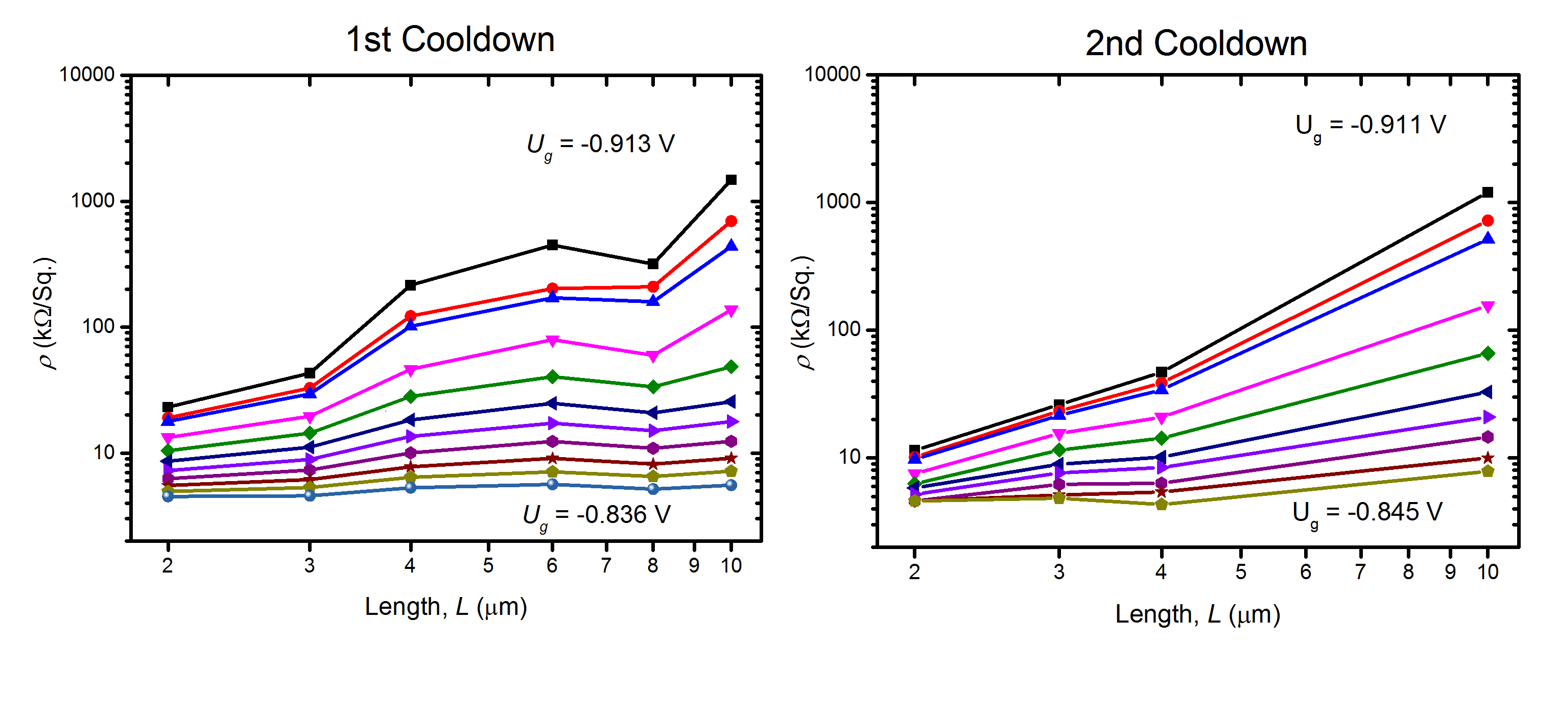
Before presenting our concluding remarks, we first consider the important issues of (i) the background disorder potential the 2DEGs reside in TripathiKennetPRB2006 ; TripathiKennetPRB2007 ; NeilsonHamitlonPRB2010 and (ii) interelectron interactions. Implicit in our analysis based on the scaling hypothesis is the assumption that the background disorder experienced by the various 2DEGs is statistically homogeneous. However, we believe this assumption to be amply justified by the systematic vs trend observed in all three sets of 2DEGs: D9, D11 and D3 SM . We have also found this trend to be reproducible between cooldowns, albeit with marginally different pinch-off characteristics SM . Thus, it seems reasonable to believe that the statistical degree of inhomogeneity in the disorder is small, perhaps responsible for the departures from perfect linearity in Figs. 2(a) and 2(b). It is also conceivable that ”fluctuations” in due to the mesoscopic nature of the 2DEGs are influencing transport SchreiberPRL1991 ; SoukoulisEconomouWRM1999 ; MirlinPhysRep2000 ; CuevasKravtsovPRB2007 . In other words, it is possible that the small scale of the 2DEG facilitates observation of certain ballistic electron trajectories which are not observable at longer length scales. However, we believe we have minimized the effect of such nonergodicities by (i) working at values where [see Fig. 3(a) and also Ref. SM ] and (ii) averaging our data over long times before recording SM . The second important point to consider is that of interelectron interactions which, importantly, must be present in the 2DEGs since the interaction parameter , which is the ratio of the Coulomb energy and kinetic energy of the electrons = , attains values as large as 5 in our studies. However, as was demonstrated recently in Ref. Mard_etal_PRL2015 , qualitative changes in are not expected even in the presence of strong interactions, and this is consistent with our findings. It will be interesting to understand whether the recently observed strong enhancement in the magnitude of measured in similar 2DEGs NarayanPRB or the observed violation of the Mott formula NarayanPRB ; NarayanNJP , where and were observed to oscillate asynchronously, reflect strong interaction effects or not. Lastly, we also wish to point out the similarities between our experimental results and the phenomenology of many-body delocalized phases in translationally-invariant 2D systems NandkishorePRB2014 . While it is debatable whether our experimental system stringently fulfills the criteria for many-body delocalization, namely complete isolation from the environment, we note that this is certainly consistent with the lack of electron decoherence even at K.
In conclusion we emphasize that the observed dependence of in mesoscopic 2DEGs is strongly consistent with the scaling hypothesis, which in turn suggests that the 2DEGs are, in fact, in the 1 regime, but perceptibly Anderson localized, i.e., with suppressed due to the finite . In macroscopic 2DEGs where , conductivity scaling may not be apparent since blocks of size contribute in an incoherent fashion. Nevertheless, it is important to note that as long as the conductivity of such a block must be diminished from its value at size , rendering imprecise the identification that . The observation of scaling-like behavior at length scales of several m and at temperatures of 10 K suggest the system under study to be remarkably robust to decoherence effects. While we do not fully understand why this might be, we speculate that this has to do with the specific device geometry SM in which the ohmic contacts are at a large spatial separation from the 2DEGs being studied. Thus, the primary link the 2DEGs have to the environment is the tenuous low- electron-phonon coupling which might be further weakened due to the narrow mesa widths employed Banerjee:2015 ; Backes:2016 . Importantly, this opens up several possibilities towards studying many-body localized electron phases Basko_etal .
We acknowledge funding from the Leverhulme Trust, UK and the Engineering and Physical Sciences Research Council (EPSRC), UK. We also acknowledge D. Joshi for assistance with device fabrication. DB and VN acknowledge useful discussions with Margarita Tsaousidou, Chris Ford, Charles Smith, Moshe Kaveh and Richard Berkovits. Supporting data for this paper is available at the DSpace@Cambridge data repository (https://www.repository.cam.ac.uk/handle/ 1810/252722).
References
- (1) E. Abrahams, P. W. Anderson, D. C. Licciardello, and T. V. Ramakrishnan, Phys. Rev. Lett. 42, 673 (1979).
- (2) F. Evers and A. D. Mirlin, Rev. Mod. Phys. 80, 1355 (2008).
- (3) See Supplemental Material at http://link.aps.org/supplemental/ 10.1103/PhysRevB.92.235427 for supporting text and additional experimental data.
- (4) E. Abrahams, S. V. Kravchenko, and M. P. Sarachik, Rev. Mod. Phys. 73, 251 (2001).
- (5) M. Y. Simmons et al., Phys. Rev. Lett. 84, 2489 (2000).
- (6) A. R. Hamilton, M. Y. Simmons, M. Pepper, E. H. Linfield, and D. A. Ritchie, Phys. Rev. Lett. 87, 126802 (2001).
- (7) M. J. Uren, R. A. Davies, M. Kaveh, and M. Pepper, J. Phys. C 14, 5737 (1981).
- (8) S. V. Kravchenko, W. E. Mason, G. E. Bowker, J. E. Furneaux, V. M. Pudalov, and M. D’lorio, Phys. Rev. B 51, 7038 (1995).
- (9) L. Li, Y. Y. Proskuryakov, A. K. Savchenko, E. H. Linfield, and D. A. Ritchie, Phys. Rev. Lett. 90, 076802 (2003).
- (10) V. M. Pudalov, M. E. Gershenson, H. Kojima, G. Brunthaler, A. Prinz, and G. Bauer, Phys. Rev. Lett. 91, 126403 (2003).
- (11) N. F. Mott and E. A. Davis, Clarendon Press, Oxford (1971).
- (12) A. L. Efros and B. I. Scklovskii, J. Phys. C: Solid State Phys. 8, L49 (1975).
- (13) R. A. Davies, M. Pepper, and M. Kaveh, J. Phys. C: Sol. Stat. Phys. 16, L285 (1983).
- (14) A. Ghosh, M. Pepper, H. E. Beere, and D. A. Ritchie, Phys. Rev. B 70, 233309 (2004).
- (15) M. Baenninger et al., Phys. Rev. Lett. 100, 016805 (2008).
- (16) R. Koushik et al., Phys. Rev. B 83, 085302 (2011).
- (17) V. Narayan et al., Phys. Rev. B 86, 125406 (2012).
- (18) V. Narayan et al., J. Low Temp. Phys. 171, 626 (2013).
- (19) M. Baenninger, A. Ghosh, M. Pepper, H. E. Beere, I. Farrer, P. Atkinson, and D. A. Ritchie, Phys. Rev. B 72, 241311(R) (2005).
- (20) S. D. Sarma and E. H. Hwang, Phys. Rev. Lett. 83, 164 (1999).
- (21) G. Zala, B. N. Narozhny, and I. L. Aleiner, Phys. Rev. B 64, 214204 (2001).
- (22) V. Narayan et al., New J. Phys. 16, 085009 (2014).
- (23) G. B. Lesovik and D. E. Khmelnitskii, Sov. Phys. JETP. 67, 957 (1988)
- (24) Ferrier et al., Phys. Rev. Lett. 93, 246804 (2004).
- (25) V. Tripathi and M. P. Kennett, Phys. Rev. B 74, 195334 (2006).
- (26) V. Tripathi and M. P. Kennett, Phys. Rev. B 76, 115321 (2007).
- (27) D. Neilson and A. R. Hamilton, Phys. Rev. B 82, 035310 (2010).
- (28) M. Schreiber and H. Grussbach, Phys. Rev. Lett. 67, 607 (1991).
- (29) C. M. Soukoulis and E. N. Economou, Waves Random Media 9, 255 (1999).
- (30) A. D. Mirlin, Phys. Rep. 326, 259 (2000).
- (31) E. Cuevas and V. E. Kravtsov, Phys. Rev. B 76, 235119 (2007).
- (32) H. Javan Mard, E. C. Andrade, E. Miranda, and V. Dobrosavljević, Phys. Rev. Lett. 114, 056401 (2015).
- (33) R. Nandkishore, Phys. Rev. B 90, 184204 (2014).
- (34) D. Backes and R. Hall and M. Pepper and H. Beere and D. Ritchie and V. Narayan, J. Phys.: Condens. Matter 28, 01LT01 (2016).
- (35) S. Banerjee and E. Altman, arXiv:1511.03676.
- (36) D.M. Basko, I.L. Aleiner, and B.L. Altshuler, Ann. Phys. 321, 1126 (2006).
Observation of geometry dependent conductivity in two-dimensional electron systems
Supplementary Material
I Equivalence of and
The Drude conductivity , where the symbols are defined in the main text. The momentum relaxation time , where is the Fermi velocity . Substituting the expression for into and rearranging, we arrive at the expression: .
However, the point we make is that according to the scaling hypothesis (Eq. (1) in the main text) the experimentally measured is almost always smaller than due to the finite extent of . Therefore, naively estimating as would result in an underestimate for , and the appropriate manner in which to estimate is from fitting the size dependence of to Eq. (1) of the main text.
II Experimental methods
II.1 Wafer details and device fabrication
The wafers used in this experiment are MBE-grown -doped structures in which the 2DEG resides 300 nm below the surface. The -dopants lie 40 nm above the 2DEG. At 4 K, the mobility of a macroscopic ( m 100 m) Hall bar sample was measured to be 220 m2/Vs with carrier density m-2.
Devices were fabricated using three stages of optical lithography. First, the conducting mesa was defined using a wet chemical etch, after which Au-Ge-Ni Ohmic contacts were deposited by therml evaporation. These were annealed at 450∘ in an atmosphere of forming gas in order for electrical contact to the buried 2DEG. Finally, Ti-Au top-gates were thermally evaporated onto the patterned sample surface. As shown schematically in Fig. (S 1), each device contains six top-gate-defined 2DEGs. The mesa was defined with two parallel arms, rather than one long one in which the 2DEGs would all be in series. This was done in order to keep the 2DEGs in close proximity to each other (to minimize variations in the background disorder), and also to avoid the large series resistance associated with long, narrow sections of mesa (see next section for further details).
II.2 Electrical measurements
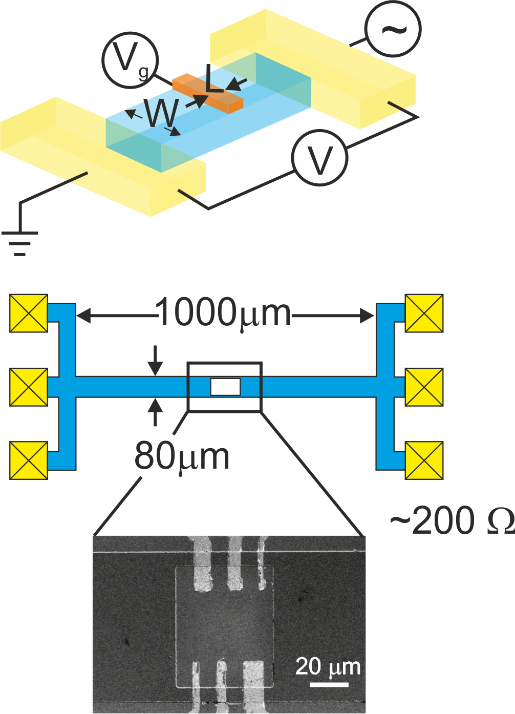
The measurements were performed between 0.3 K and 10 K in a He-3 cryostat equipped with a superconducting magnet. Devices were cooled down from room temperature to 4 K over a period of 20 hours and only 2DEGs that were cooled down simultaneously were compared against each other. Each 2DEG was addressed individually with a DC voltage source. When a particular 2DEG was being measured, a large negative (-5 V) was applied to all three gates on the adjacent mesa arm in order to completely cut off any parallel conduction. We ascertained that the resistance of the adjacent arm was G using a Keithly 236 Source-Measure unit.
Electrical measurements were made in a quasi-four-terminal setup (see below) using an excitation current 100 pA at frequency Hz. We ascertained that there was no appreciable joule heating by increasing to 1 nA, and noting no change in the experimental data. Our measurements are performed by sweeping the gate voltage slowly such that each data point is averaged for several (10 – 100) seconds before recording.
There are several factors that we had to carefully consider when measuring the mesoscopic 2DEGs:
1. From the device design it is clear that there are ungated sections of the mesa that contribute to the resistance measurement, i.e., there is an extra ‘lead’ resistance . At V, (the measured resistance), the approximation arising from not excluding the 2DEG area. However, as seen from Fig. S 1, this corresponds to an error of , corresponding to the length of the 2DEG (at most 10 m) divided by the length of the entire mesa (1000 m). This therefore allows us to subtract ( 200 in all the devices) to estimate the true 2DEG resistance . Clearly this approximation becomes less reliable as , due to which we restrict our analysis to large .
2. A second reason to restrict the analysis to high is to minimize any ballistic electron effects that might be significant when . At V, the mobility and carrier density correspond to m which is larger than the largest 2DEG investigated in this study. By confining the analysis to V, the 2DEGs are always in a regime where , i.e., where the electronic motion is diffusive.
3. And finally, we note that there will be electric-field fringing at the edges of the top-gate defined 2DEGs. However, we expect these to be of the order of the 2DEG setback distance = 300 nm and, moreover, that these will contribute a constant offset to each 2DEG and therefore, not influence the results in a major way.
The 2DEG resistivity is defined as and based on the above arguments, we are confident that this is a meaningful definition bereft of any artifacts due to inhomogeneities, ballistic electron trajectorites, or even surface/boundary scattering. The last of these follows from point 2 where we argue that the electrons have a well-defined diffusivity.
III Extra supporting data