Topological Nodal-Line Fermions in the Non-Centrosymmetric Superconductor Compound PbTaSe2
Abstract
In a typical three-dimensional metal, the low-energy excitations are found on a two-dimensional closed Fermi surface in momentum space. Topological semimetals, by contrast, can support one-dimensional Fermi lines or zero-dimensional Fermi-Weyl points, at locations in momentum space, where the valence and conduction bands touch. While the degeneracy points in Weyl semimetals are protected against any perturbation that preserves translational symmetry, nodal lines are topologically protected by symmetries such as mirror reflection. Here we report on the existence of topological nodal-line states in the non-centrosymmetric compound single-crystalline PbTaSe2 with strong spin-orbit coupling. Remarkably, the spin-orbit nodal lines in PbTaSe2 are not only protected by the reflection symmetry but also characterized by an integer topological invariant as we show here. Our detailed angle-resolved photoemission (ARPES) measurements, first-principles simulations and theoretical analysis illustrate the physical mechanism underlying the formation of the topological nodal-line states (TNLS, in contrast to Weyl Semimetals) and associated surface states for the first time. Therefore, this work paves the way towards exploring the exotic properties of the topological nodal-line fermions in condensed matter systems and, potentially, the rich physics arising from the interplay between the topological nodal-line states and the emergent superconductivity we report in the single crystal phase phase of this compound.
The discovery of the time-reversal invariant topological insulator has stimulated enormous research interests in novel topological states protected by symmetries RMP ; Zhang_RMP ; Book . One of the key properties of topological materials is the existence of symmetry-protected metallic edge or surface modes in bulk-insulating ground states which is due to a topologically nontrivial ordering of bulk wave functions. Recently, due to the experimental observations of Weyl semimetals Wan2011 ; Burkov2011 ; HgCrSe ; Thallium ; Hsin_TaAs ; Dai_TaAs ; Hasan_Na3Bi ; Nagaosa , the research interest in topological phenomena in condensed matter systems has partially shifted to from insulators to semimetals and metals. A Weyl semimetal is a topological state of matter whose low-energy bulk electrons are linearly dispersing Weyl fermions. The two-fold degenerate Weyl nodes, carrying non-zero chiral charge, are connected on the boundary by Fermi arc surface states, which are predicted to exhibit unusual transport behaviors Hosor ; NMR ; Franz2013 ; Ojanen . In contrast to Weyl semimetals whose bulk Fermi surface has dimension zero, topological nodal-line semimetals have extended band touching along one-dimensional curves in space, presenting a significant expansion of topological materials beyond topological insulators and Weyl semimetals, and new opportunities to explore exotic topological nodal physics. Line-like touchings of a conduction and valence band require extra symmetries besides translation, such as mirror reflection, to be topologically protected. Kinematically this protection involves a finite fraction of Brillouin zone. For this reason, this leads potentially to many anomalies in their electromagnetic and transport response BurkovNL ; Phillips ; Chiu . Similar to the case of Weyl nodes, one can define an integer topological invariant for the line node along which two nondegenerate bands touch Chiu . Despite the many theoretical discussions of nodal-line semimetals, a material realization of topological nodal-line fermions has been lacking for many years just like Weyl semimetals. Here we report the existence of topological nodal-line phase in the normal states of the superconducting compound PbTaSe2 for the first time.
The crystal lattice of PbTaSe2 lacks space inversion symmetry, which lifts the spin-degeneracy of its electronic bulk bands. Our angle-resolved photoemission (ARPES) measurements together with DFT calculations show that the conduction band originated from Pb- orbitals and the valence band from Ta- orbitals cross each other, forming three nodal-line states close to the Fermi energy. The nodal lines are protected by a reflection symmetry of the space group as we show. The topological-nodal-line state in PbTaSe2 belongs to the symmetry class A () of symmetry-protected semimetals Chiu . We also demonstrate through effective Hamiltonian modeling and DFT simulations that the nodal lines are accompanied by unique surface bands. These topological surface states are due to the Berry phase agglomerated around the nodal line in analogy to the states on the graphene-like zigzag edge. Our experimental and theoretical results establish a material realization of topological nodal-line fermions in the superconducting compound PbTaSe2. The findings reported here are of substantial importance because the door for exploring the exotic properties of nodal-line states in condensed matter and, potentially, the rich physics arising from the interplay of nodal lines and emergent superconductivity has been opened by the identification of this compound.
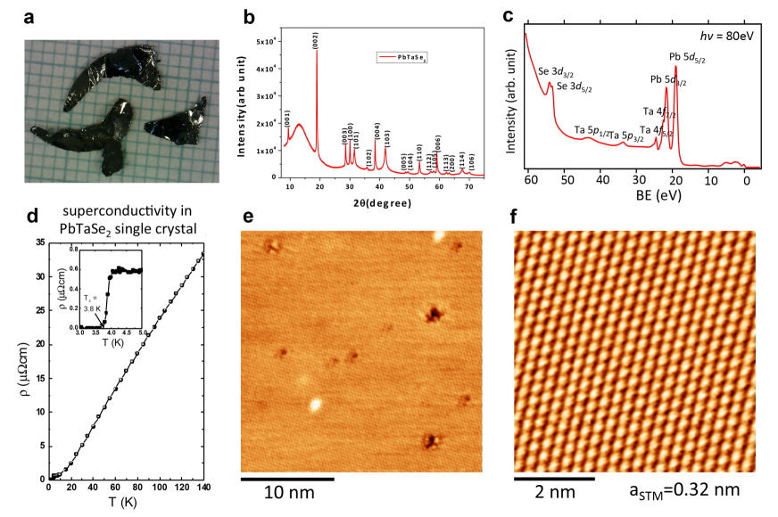
Our PbTaSe2 single crystals were prepared by the chemical vapor transport (CVT) method, see Fig. 1a. The samples were of high structural quality, which was confirmed by our X-ray diffraction (XRD) and scanning tunneling microscopy (STM) measurements. The XRD peaks shown in Fig. 1b are consistent with the space group of PbTaSe2, (187), and, therefore demonstrating the lack of inversion symmetry of our PbTaSe2 single crystals. This is crucially important for lifting the spin degeneracy, a necessary condition for the formation of topological nodal lines. To further check the chemical composition of our samples, we performed a photoemission core level scan. Clear Pb-, Ta- and Se- core level peaks were observed in the photoemission spectrum, which confirms the correct chemical composition in our PbTaSe2 single crysta samples, shown in Fig. 1c. To verify the superconducting property of our samples, a transport measurement was carried out. The measured resistivity curve, Fig. 1d, shows a clear superconducting transition temperature at 3.8 K, consistent with the value reported in Cava . Figures 1e and 1f show STM images of the cleaved (001) surface. The topography image clearly reveals a hexagonal lattice with few defects, demonstrating the high quality of our samples. Furthermore, no surface reconstruction was observed on the cleaved surface. The high-resolution STM topography yields a lattice constant of 3.2 Å.
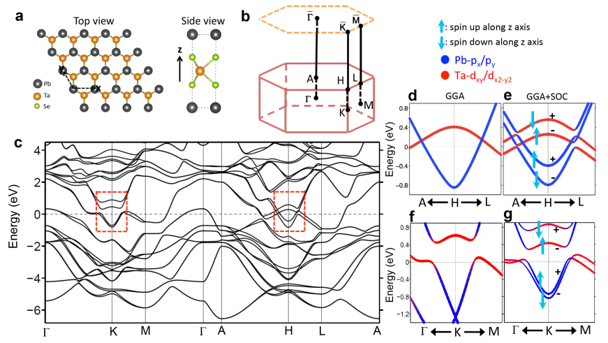
PbTaSe2 crystalizes in a hexagonal lattice system in which the unit cell consists of one Pb, one Ta and two Se atoms and each atom resides on a hexagonal flat layer, shown in Fig. 2a. The stacking sequence of these atomic planes within the unit cell is Pb-Se-Ta-Se: A-A-B-A (A, B and C, here, refer to the three high-symmetry spots on a hexagonal lattice). The lattice can also be viewed as a Pb-layer intercalating two adjacent TaSe2 layers with Pb atoms sitting above Se atoms. The Pb intercalation suppresses the softening of phonon modes associated with the charge density wave (CDW) in TaSe2 and stabilizes the hexagonal lattice on the surface Tay-Rong . This particular stacking does not preserve the space inversion symmetry, but the lattice is reflection-symmetric with respect to the Ta atomic plane. In other words, the Ta atomic planes are a mirror plane of the crystal lattice under the mirror operation that sends to . This reflection symmetry of the lattice provides a protection for the topological nodal lines, as discussed later on. The bulk and (001)-projected surface Brillouin zones are shown in Fig. 2b. The A, H and L points are high symmetry points on the plane, which is a mirror plane of the bulk Brillouin zone. Figure 2c presents an overview of the band structure calculation for PbTaSe2, which was performed by the DFT-GGA method. Close to the Fermi level, two prominent features in the band structure are observed. One is a giant hole pocket around , whose states are mainly derived from the Ta 5 orbitals that are oriented out of the Ta atomic plane, taking the Ta plane as the plane. The second major contribution to the density of states at the Fermi level comes from the four bands that cross each other near H. The two electron-like conduction bands originate from Pb-6 orbitals and the two hole-like valence bands from Ta- orbitals. We note that all these orbitals are invariant under . A zoom-in view of the bands around H without/with spin-orbit coupling (SOC) is shown in Fig. 2d and 2(e), respectively. Without the inclusion of SOC, the conduction and valence bands become spin-degenerate. The two bands belong to different representations of the space group (the representation of the electron-like band is A′ and that of the hole-like band is A′′), therefore the intersection of the two bands is protected by the crystalline symmetry, forming a spinless nodal ring. Once SOC is turned on, each band split into two spin branches with opposite spin orientations and mirror reflection eigenvalues as indicated in Fig. 2e. Only the crossings of branches with opposite mirror reflection eigenvalues remain gapless as a result of symmetry protection, forming a pair of nodal rings. Interestingly, SOC also gives rise to a third nodal ring on plane. The detailed band dispersion and the rise of three nodal rings are very well captured by our effective Hamiltonian, please see SI . Before proceeding to a detailed discussion of the nodal-line states, we will present the results of our ARPES measurement, verifying the overall band dispersion of Pb conduction bands and Ta valence bands obtained from our DFT calculation.
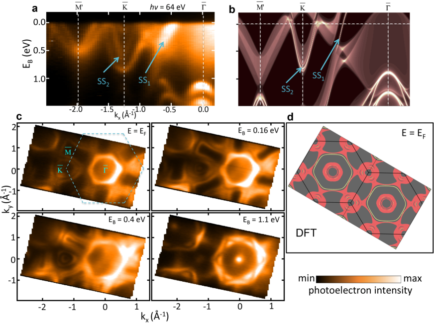
Fig. 3a shows a brief overview of our ARPES band mapping and the corresponding numerical calculation of the PbTaSe2 band structure is presented in Fig. 3b. The projected bulk bands and surface bands (as highlighted by white lines) were calculated for the Pb-terminated (001) surface. The DFT band structure reproduces the ARPES spectrum very well. Specifically, in the ARPES spectral cut, a band marked as SS1 with high intensity poke the Fermi level between and . This is the surface state band associated with the Pb-terminated (001) surface SI . Around there are three concave bands whose binding energy at are 0.21, 0.75, and 0.80 eV, respectively. The top and bottom bands correspond to the electron-like bands derived from Pb- orbitals. The middle band, marked as SS2, is consistent with the surface band as plotted in Fig. 3b. The two bands at are tails of the two Ta- bands that cross the two Pb- bands forming the nodal rings in the vicinity of . Two Ta- bands have to degenerate in energy at according to the Kramers theorem. The ARPES measured (001) Fermi surface with the incident photon energy of 64 eV and the theoretical simulation are shown in Figs. 3c and 3d, respectively. At the Fermi level, our data shows that the Fermi surface consists of three parts: a hexagon-shaped pocket centered at with smeared intensity inside, a dog-bone shaped contour centered at the point and several circles surrounding the point. Our ARPES data and calculation show agreement on those features. Furthermore, the hexagon centered at and the intensity inside are the surface band and the bulk hole pocket at , respectively. The dog-bone shaped contour corresponds to the one branch of the Ta valence band and the circles around are from the other branch of the Ta valence band, the surface states and the spin-split conduction band derived from Pb orbitals. As the binding energy decreases we find that the Pb pockets at shrink while the Ta pockets expand outwards, which is in good accordance with the characteristics of the electron-like Pb bands and hole-like Ta bands.
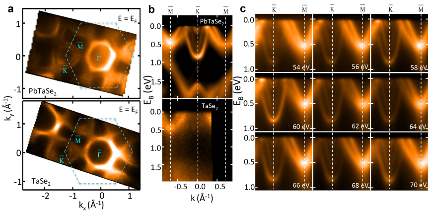
TaSe2 can be regarded as a building block of PbTaSe2, and therefore its electronic structure can be traced from that of PbTaSe2. To highlight the difference between electronic structure of TaSe2 and PbTaSe2, we mapped out the Fermi surface and band structure along of the two compounds, shown in Figs. 4a and 4b. In the Fermi surface mapping of TaSe2, there are one dog-bone shaped contour centered at and only one circle shaped contour centered at . Those contours are from Ta valence bands, and consistent with previous work Balu . By contrast, the Fermi surface of PbTaSe2 has more ring-shaped contours centered at , signifying the contribution from the Pb layers. It is easier to view this difference from the cut. TaSe2 does not show any electron-like bands at that exist in PbTaSe2. Fig. 4c shows the ARPES mapping of the Pb and Ta bands of PbTaSe2 with photon energies from 54 eV to 70 eV. The middle band at does not show any photon-energy dependence, which is consistent with the surface nature of this band. However the other bands at and don’t exhibit obvious changes with different photon energies either. This seems to contradict to the assignment of those band as bulk bands according to our DFT calculations. The inconsistency can be understood by considering the fact that the Pb-6 and Ta- orbitals that constitute those bands are primarily confined within the Pb and Ta atomic planes (which are parallel to the plane), and, thus, the interlayer couplings (say, the coupling of one Pb-6 orbital with another orbital on the adjacent Pb plane) is largely suppressed, which results in little /photon-energy dependence.
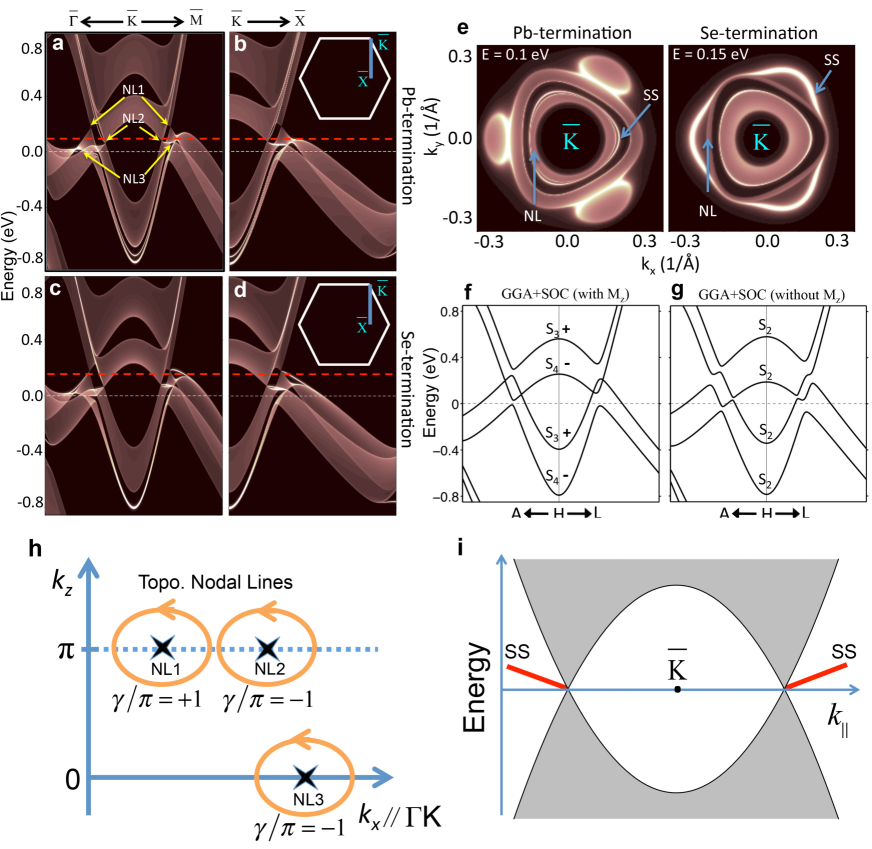
From the discussion before, we know that the electron-like bands from the intercalated Pb layers are the essential component for forming the topological-nodal-ring band structure. By comparing with the TaSe2 spectrum, our ARPES established unambiguously the existence of the Pb bands. To further examine the topological-nodal-line states and associated surface states, we calculated the band structure for Pb- and Se-terminated surfaces as shown in Figs. 5a-d. The projected bulk band on each cut from shows three nodal points at 0.05 eV, 0.15 eV, and 0.03 eV above the Fermi level. The first two closer to lie on the plane while the third one is on the plane. Let us refer to these three nodal lines as NL1, NL2 and NL3. Corresponding nodal points can be found on a cut of arbitrary orientation that includes . For example, the band structure along a generic direction is shown in Figs. 5b and 5d. Unlike the projected bulk band which is independent of surface termination, the dispersion of surface bands is found to be sensitive to the surface condition. However, in both cases we do find a surface band connecting to each nodal line, indicative of the topological nature of the bulk nodal lines. In the Pb-termination case, the surface bands disperse outwards with respect to , from NL1. The surface band connecting to NL2 grazes inwards at the edge of the lower bulk Dirac cone and merge into the bulk band. The surface band from NL3 disperses inwards with respect to , consistent with the “SS2” band in our ARPES spectrum in Fig. 3, which forms a “drumhead” surface state contour. By contrast, on the Se-terminated surface the surface band connecting to NL2 first moves into the bulk band gap and then fall into the bulk band region. The surface band from NL1 disperses outwards and connects to NL3. Please refer to SI for a detailed visualization of connection of the surface bands to the bulk nodal lines. To get an overall view of the nodal ring and surface band, we plot in Fig. 5e the isoenergy contour in the vicinity of the NL1 nodal ring of the Pb-terminated surface and the NL2 nodal ring of the Se-terminated surface, as indicated by the red dashed lines in Figs. 5a-d. Indeed, gapless nodal points and surface states can be found at every in-plane angle departing from . These nodal rings are protected against gap opening by the crystalline symmetry. Specifically, the states in the two Pb branches belong to two different representations of the space group, namely S3 and S4 as shown in Fig. 5f. The same is true for the two Se branches. In particular, with respect to the Ta atomic plane, the two representations have opposite mirror eigenvalues under the reflection operation. Therefore, gap opening is forbidden at the crossing point between two branches of different mirror eigenvalues, which results in the nodal rings discussed in this work. In this sense, the nodal rings is under the protection of the reflection symmetry. If we shift the Pb atom slightly in the vertical direction thus breaking the reflection symmetry, all of the four branches are found to belong to the same representation of the reduced space group and, in this case, a gap opening is allowed at every crossing point of these branches as illustrated in Fig. 5g. A similar gap opening is also found in NL3 on plane upon breaking the reflection symmetrySI .
Let us briefly discuss the topological characterization of the nodal lines and the origin of the surface bands. The material PbTaSe2 is time-reversal symmetric, with time-reversal symmetry is represented by , where denotes complex conjugation and is the second Pauli matrix acting on the electron spin. The mirror symmetry acts in spin space as and therefore anticommutes with . This would place PbTaSe2 in class AII- in the classification of Chiu . However, since the nodal lines are centered around momenta / and / which are not invariant under time-reversal, but pairwise map into each other, the time-reversal symmetry imposes no constraints on the nodal lines individually. The material has therefore to be classified according to the time-reversal breaking class A- which admits a integer topological classification for Fermi surfaces of codimension 2, i.e., lines ( in Chiu ). The nodal lines carry a topological quantum number , which is given by the difference in the number of occupied bands with eigenvalue inside and outside the line. In the case at hand, for the nodal line (NL3) in the plane, while (NL1) and (NL2) for the two nodal lines in the plane. We have also computed numerically under the DFT framework the winding number , where is the Berry connection of the occupied Bloch bands . For a closed loop encircling any of the nodal nodal lines, we find that with the same sign as of that line, as shown in Fig. 5h.
The topological origin of the observed surface states is rather subtle. Surface states associated with the topological invariant via the bulk-boundary correspondence should only appear on surfaces that preserve . The (001) surface, however, breaks . The reason why we still observe surface states can be understood from the Berry phase of around the nodal line and the analogy to the edge states on the zigzag edge of graphene. Consider the bulk Hamiltonian on a plane in momentum space that contains both and . At low energies, each nodal ring pierces this plane twice giving rise to two Dirac cones in this Hamiltonian. These two cones have a Berry phase and with respect to the orientation of the plane, precisely as in (spinless) graphene, as schematically depicted in Fig. 5i. We know that for any termination of a graphene sample, an edge state emanates from the projection of each of the Dirac points in the edge Brillouin zone (except for the pathological case where both Dirac points project on the same spot in the edge Brillouin zone). By this analogy, we also expect these edge states to emanate from the surface projections of the nodal lines in any direction away from the point, thereby forming a surface band. We note that the dispersion of this band and even whether it appears inside or outside the projection of the nodal line is not universal and depends on the details of the surface termination.
Recently, some preprint theoretical works have reported on Ca3P2 and Cu3PdN proposing there may be nodal-line states Ca3P2 ; CuPdN . We note that our work is distinct from those works in three aspects: (1) Both Ca3P2 and Cu3PdN are centrosymmetric and, therefore, due to the coexistence of time-reversal and inversion symmetry, have four-fold degeneracy at the nodal ring. By contrast, the degeneracy of nodal-ring states is two in PbTaSe2 due to the lack of inversion symmetry. (2) In Ca3P2 and Cu3PdN, the nodal-line states exist only in the absence of SOC. In real materials SOC, however, always exists. In PbTaSe2, SOC is essential ingredient for the formation of nodal-ring states. (3) Our ARPES measurement established an experimental characterization of the topological nodal-line material PbTaSe2.
In summary, our direct experimental observation by ARPES of the coexistence of Pb concave bands and Ta convex bands centered at in the non-centrosymmetric superconductor PbTaSe2 is in good agreement with our first-principles band structure calculations, establishing the realization of the unusual ring-shaped topological-nodal-line states in this compound. The topological nodal rings are protected by the reflection symmetry of the system. Meanwhile, the nodal rings are uniquely associated with “drumhead”-like surface states in a manner that resembles the connections of edge states and the nodal points in graphene. Considering the nodal characteristics shared by topological nodal-line states and Weyl semimetals, it is very likely that the topological nodal-line materials exhibit much of the long-sought out exotic properties of Weyl semimetals, but with additional non-trivial features. For example, nodal-line states possess an extra degree of freedom for manipulating novel properties of Weyl materials, which is the finite size of the nodal line. Furthermore, interaction-induced instabilities that have been broadly discussed for Weyl semimetals should be more likely occurring in nodal-line states due to the higher density of states at the Fermi energy. In addition, superconductivity is induced by intercalating Pb layers to TaSe2, which also offers the essential ingredient, the Pb conducting orbitals, for the formation of the topological nodal-line states. Considering the intrinsic superconductivity, the spin-split bulk nodal-line band structure and the nontrivial surface states close to the Fermi level, it is possible that helical superconductivity and -wave Cooper pairing may exist in this compound without the aid of the proximity effect Kane ; Suyang . Therefore, novel physics may arise from the interplay of the nodal-line states and the emergent superconductivity of PbTaSe2, which calls for further experimental investigation on PbTaSe2. Our ARPES measurements, detailed DFT simulation and theoretical analysis demonstrate the fundamental mechanism for realizing topological nodal-line fermions in PbTaSe2, and pave the way for exploring the exotic properties of topological nodal-line states in condensed matter systems.
I Methods
Single crystals of PbTaSe2 were grown by the CVT method using chlorine in the form of PbCl2 as a transport agent. For the pure synthesis of PbTaSe2, stoichiometric amounts of the elements (purity of Pb and Ta: 6N, of Se: 5N) were loaded into a quartz ampoule, which was evacuated, sealed and fed into a furnace (850) for 5 days. About 10 g of the prereacted PbTaSe2 were placed together with a variable amount of PbCl2 (purity 5N) at one end of another silica ampoule (length 30-35 cm, inner diameter 2.0 cm, outer diameter 2.5 mm,). All treatments were carried out in an Argon box, with continuous purification of the Argon atmosphere resulting in an oxygen and water content of less than 1 ppm. Again, the ampoule was evacuated, sealed and fed into a furnace. The end of the ampoule containing the prereacted material was held at 850 , while the crystals grew at the other end of the ampoule at a temperature of 800 (corresponding to a temperature gradient of 2.5 K/cm) during a time of typically 1 week. Compact single crystals of sizes of up to 8 5 5 mm3 were obtained.
ARPES measurements were performed at the liquid nitrogen temperature in the beamline I4 at the MAX-lab in Lund, Sweden. The energy and momentum resolution was better than 20 meV and 1 of the surface Brillouin zone (BZ) for ARPES measurements at the beamline I4 at the MAX-lab. Samples were cleaved in situ under a vacuum condition better than 1 10-10 torr. Samples were found to be stable and without degradation for a typical measurement period of 24 hours.
STM experiments were conducted with a commercial system (Unisoku). Samples were cleaved at room temperature in a vucuum better than 2 10-10 mbar and transferred to a STM head precooled to 77 K. Constant-current mode STM images were taken with chemical etched Pt/Ir tips. Bias voltages were applied to samples.
We computed electronic structures using the norm-conserving pseudopotentials as implemented in the OpenMX package within the generalized gradient approximation (GGA) schemes Perdew ; Ozaki . Experimental lattice constants were used Eppinga . A 12 12 4 Monkhorst-Pack k-point mesh was used in the computations. The SOC effects are included self-consistently Theurich . For each Pb atom, three, three, three, and two optimized radial functions were allocated for the , , , and orbitals (), respectively, with a cutoff radius of 8 Bohr. For each Ta atom, was adopted with a cutoff radius of 7 Bohr. For each Se atom, was adopted with a cutoff radius of 7 Bohr. A regular mesh of 300 Ry in real space was used for the numerical integrations and for the solution of the Poisson equation. To calculate the surface electronic structures, we constructed first-principles tight-binding model Hamilton. The tight-binding model matrix elements are calculated by projecting onto the Wannier orbitals Weng . We use Pb , Ta and , and Se orbitals were constructed without performing the procedure for maximizing localization.
II Acknowledgements
We gratefully acknowledge C. M. Polley, J. Adell, M. Leandersson, T. Balasubramanian for their beamline assistance at the Maxlab. We also thank A. P. Schnyder, C. Fang and M. Franz for discussions. T.R.C. acknowledges visiting scientist support from Princeton University.
References
- (1) Hasan, M. Z., Xu, S.-Y. & Neupane, M. Topological Insulators, Topological Dirac semimetals, Topological Crystalline Insulators, and Topological Kondo Insulators. Topological Insulators: Fundamentals and Perspectives, (John Wiley & Sons) (2015). Preprint at http://arxiv.org/abs/1406.1040 (2014).
- (2) Hasan, M. Z. & Kane, C. L. Topological insulators. Rev. Mod. Phys. , 3045-3067 (2010).
- (3) Qi, X.-L. & Zhang, S.-C. Topological insulators and superconductors. Rev. Mod. Phys. , 1057-1110 (2011).
- (4) Wan, X., Turner, A. M., Vishwanath, A. & Savrasov, S. Y. Topological Semimetal and Fermi-arc surface states in the electronic structure of pyrochlore iridates. Phys. Rev. B 83, 205101 (2011).
- (5) Burkov, A. A. & Balents, L. Weyl semimetal in a topological insulator multilayer. Phys. Rev. Lett. 107,127205 (2011).
- (6) Singh, B., Sharma, A., Lin, H., Hasan, M. Z., Prasad, R. & Bansil, A. Topological electronic structure and Weyl semimetal in the TlBiSe2 class of semiconductors. Phys. Rev. B , 115208 (2012).
- (7) Xu, G. et al., Chern semi-metal and quantized anomalous Hall effect in HgCr2Se4. Phys. Rev. Lett. 107, 186806 (2011).
- (8) Huang, S.-M., Xu, S.-Y. et al., An inversion breaking Weyl semimetal state in the TaAs material class. http://arxiv.org/abs/1501.00755 (2015).
- (9) Xu, S.-Y. et al. Observation of Fermi arc surface states in a topological semimetal. Science , 294-298 (2015).
- (10) Weng, H., et al. Weyl semimetal phase in non-centrosymmetric transition metal monophosphides. http://arxiv.org/abs/1501.00060 (2015).
- (11) Yang, B.-J. & Nagaosa, N. Classification of stable three-dimensional Dirac semimetals with nontrivial topology. Nat. Commun. , 4898 (2014).
- (12) Hosur, P. Friedel oscillations due to Fermi arcs in Weyl semimetals. Phys. Rev. B , 195102 (2012).
- (13) Son, D. T. & Spivak, B. Z. Chiral anomaly and classical negative magnetoresistance of Weyl metals. Phys. Rev. B , 104412 (2013).
- (14) Vazifeh, M. M. & Franz, M. Electromagnetic response of Weyl semimetals. Phys. Rev. Lett. 111,027201 (2013).
- (15) Ojanen, T. Helical Fermi arcs and surface states in time-reversal invariant Weyl semimetals. Phys. Rev. B , 245112 (2013).
- (16) Chiu, C. & Schnyder, A., Classification of reflection symmetry protected topological semimetals and nodal superconductors. Phy. Rev. B 90, 205136 (2014).
- (17) Burkov, A. A., Hook,M. D. & Balents L. Topological nodal semimetals. Phys. Rev. B 84, 235126 (2011).
- (18) Phillips M. & Aji V. Tunable line node semimetals. Phys. Rev. B 90, 115111 (2014).
- (19) Ali, Mazhar N. et al. Noncentrosymmetric superconductor with a bulk three-dimensional Dirac cone gapped by strong spin-orbit coupling. Phys. Rev. B 89, 020505(R) (2014).
- (20) Chang, T.-R. et al. unpublished.
- (21) Please see the supplementary online information.
- (22) Laverock, J. et al. -resolved susceptibility function of 2-TaSe2 from angle-resolved photoemission. Phys. Rev. B 88, 035108 (2013).
- (23) Xie, L. S., et al. Potential ring of Dirac nodes in a new polymorph of Ca3P2. http://arxiv.org/abs/1504.01731 (2015).
- (24) Yu, R., et al. Topological Node-Line Semimetal and Dirac Semimetal State in Antiperovskite Cu3PdN. http://arxiv.org/abs/1504.04577 (2015).
- (25) Fu, L. & Kane, C. L. Superconducting proximity effect and Majorana fermions at the surface of a topological insulator. Phys. Rev. Lett. 100, 096407 (2008).
- (26) Xu, S.-Y. et al. Momentum-space imaging of Cooper pairing in a half-Dirac-gas topological superconductor. Nat. Phys. 10, 943-950 (2014).
- (27) Perdew, J. P. Burke, K. & Ernzerhof, M. Generalized Gradient Approximation Made Simple. Phys. Rev. Lett. , 3865 (1996).
- (28) Ozaki, T. Variationally optimized atomic orbitals for largescale electronic structures. Phys. Rev. B , 155108 (2003).
- (29) Eppinga, R. & Wiegers, G. A. A generalized schene for niobium and tatalum dichalcogenides intercalated with pos-transition elements. Physica B and C , 121 (1980).
- (30) Theurich, G. & Hill, N. A. Self-consistent treatment of spin-orbit coupling in solids using relativistic fully separable ab initio pseudopotentials. Phys. Rev. B , 073106 (2001).
- (31) Weng, H., Ozaki, T. & Terakura, K. Revisiting magnetic coupling in transition-metal-benzene complexes with maximally localized Wannier functions. Phys. Rev. B , 235118 (2009).
