Impact of low-dose electron irradiation on n+p silicon strip sensors
Abstract
The response of silicon strip sensors to electrons from a 90Sr source was measured using a multi-channel read-out system with 25 ns sampling time. The measurements were performed over a period of several weeks, during which the operating conditions were varied. The sensors were fabricated by Hamamatsu Photonics K. K. on 200 m thick float-zone and magnetic-Czochralski silicon. Their pitch was 80 m, and both -stop and -spray isolation of the strips were studied. The electrons from the 90Sr source were collimated to a spot with a full-width-at-half-maximum of 2 mm at the sensor surface, and the dose rate in the SiO2 at the maximum was about 50 Gy/d. After only a few hours of making measurements, significant changes in charge collection and charge sharing were observed. Annealing studies, with temperatures up to C and annealing times of 18 hours, showed that the changes can only be partially annealed. The observations can be qualitatively explained by the increase of the positive oxide-charge density due to the ionization of the SiO2 by the radiation from the source. TCAD simulations of the electric field in the sensor for different oxide-charge densities and different boundary conditions at the sensor surface support this explanation. The relevance of the measurements for the design of strip sensors is discussed.
1 Introduction
Today, segmented silicon detectors with a spatial resolution of approximately m are used in precision tracking detectors closest to the interaction point of most collider experiments. They contribute to practically all physics analyses and were essential for the discovery of the Higgs boson and many other important physics results from the four large-scale CERN-LHC experiments. They have demonstrated an extraordinary performance with respect to precision, efficiency and reliability. The High-Luminosity LHC upgrade (HL-LHC) poses further challenges with respect to track density and radiation exposure: For an anticipated integrated luminosity of 3 000 fb-1, hadron fluences of up to neq/cm2 (1 MeV equivalent neutrons/cm2) at a distance of about 5 cm from the beam are expected from simulations, causing radiation damage to the silicon crystal and ionization doses of order 1 MGy, resulting in surface damage to the insulating layers of the sensors. Whilst silicon-bulk damage has been studied extensively, only limited knowledge of surface damage to high-ohmic silicon [1] and its interplay with bulk damage is available.
In this paper the effects of ionizing radiation for dose values between 0 and 1 kGy on the charge collection properties of strip sensors are studied using electrons from a 100 MBq 90Sr source. The relevance of the results for the HL-LHC upgrade is discussed. More details about the measurements and the results can be found in Refs. [2, 3]. Some of the results have been presented at TIPP 2014 [4].
2 Experimental setup and sensors investigated
Two different types of mini strip sensors from the CMS-HPK Campaign [5] have been investigated: One with -spray and one with -stop implants between the readout strip implants. Fig. 1 shows a top view and a cross section of a -stop sensor. The layout of the -spray sensors is identical, except that the two narrow -stop implants are replaced by a uniform implant, which covers the entire region between the -strip implants.
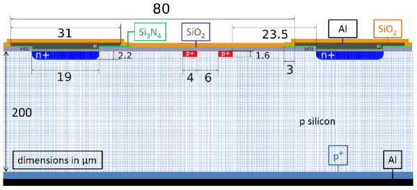
The sensors were built on 200 m-thick float-zone (FZ) silicon with a boron doping of cm-3, as determined from capacitance voltage measurements, and an oxygen concentration varying between and cm-3, as well as on magnetic-Czochralski (MCz) silicon with similar bulk doping, but with a one order of magnitude higher oxygen concentration [2]. The 64 -coupled readout strips each have a length of 25 mm, a pitch of 80 m, and are made up of 19 m-wide implants isolated from the Al strips by 250 nm of SiO2 and 50 nm of Si3N4. The Al strips overlap the 650 nm thick SiO2 layers, which cover the region between the strips, by 6 m, and the entire sensor, with the exception of the bond pads, is covered by an additional 500 nm of SiO2 for passivation. The values for the actual dopant concentrations are only poorly known. To the best of our knowledge the integrals of the dopant concentrations are cm-2 for the -stop and cm-2 for the -spray implants, respectively. The stops are two 4 m wide implants at 6 m separation centered between the readout strips.
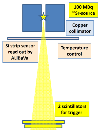
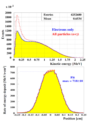
Fig. 2(a) shows the measurement setup. A 100 MBq 90Sr source, placed in a copper collimator and mounted on a computer controlled --translation table, irradiated the silicon sensor, which was mounted on a Peltier element for temperature control between C and C. The sensor was read out by ALiBaVa [6], a multi-channel readout system for silicon strip sensors with a sampling time of 25 ns. Two 3 mm-thick plastic scintillators, placed 58 and 62 mm from the source, respectively, provided the trigger signal from electrons that have traversed the silicon sensor and deposited energy in both scintillators. The energy distribution of the electrons and photons and the spatial distribution of the rate of energy-loss density in the SiO2 layer on the surface of the sensor were estimated with a Monte Carlo simulation based on GEANT3 and are shown in Fig. 2(b). The dose-rate distribution is circular with a diameter at full-width-half-maximum of 2 mm and a value at the maximum of 50 Gy/d. The non-ionizing energy-loss (NIEL) rate, relevant for radiation damage in the silicon bulk, corresponds to about neq /(cmd). The simulated energy-loss distribution of the trigger electrons in the silicon sensor is similar to a Landau distribution for minimum-ionizing-particles (mip), with a most-probable-value (mpv) of 56 keV, compared to 54 keV for mips. The angular spread of the trigger electrons is about mrad.
In this paper we study the change of the charge collection as a function of the dose from the 90Sr source of a non-irradiated -stop sensor, a non-irradiated -spray sensor, and a -stop sensor irradiated by neq/cm2 24 GeV/c protons and neq/cm2 reactor neutrons, which corresponds to an ionizing dose in SiO2 of about 0.75 MGy. This is approximately the radiation exposure expected for the CMS experiment at the HL-LHC 15 cm from the beams after an integrated luminosity of 3 000 fb-1 has been delivered [7, 8]. Both dose and NIEL rates from the 90Sr source are more than an order of magnitude lower than the maximum rates expected at the HL-LHC. If not stated otherwise, the measurements presented in this paper were performed at C, the temperature at which the silicon sensors are intended to be operated at the HL-LHC.
3 Analysis
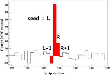
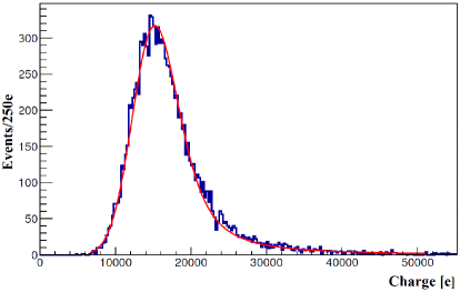
In the offline analysis events are selected if the trigger signal was in phase within ns with the 40 MHz ALiBaVa clock. Fig. 3(a) shows the pulse height (PH) versus strip number after pedestal and common mode subtraction for a typical event [2]. The strip with the largest PH is called the seed, whilst its largest neighbour defines the region of passage of the electron. These 2 strips, together with the 2 next-to-next neighbours are the 4 strips used in the analysis of an event. They are labeled -1, , , and +1, respectively. Fig. 3(b) shows the distribution of the sum of the pulse heights of the 4 strips, PH(4-cluster), in units of electron charge, e, for 5 000 events measured using a non-hadron-irradiated sensor after pedestal and common-mode subtraction. The calibration [2] uses the charge injection feature of the ALiBaVa readout system, which has an accuracy of better than 1 %. As expected from the simulation, the distribution can be fitted using the convolution of a Landau distribution with a Gaussian, which is shown as the smooth curve in Fig. 3(b). In subsequent analyses, however, we will use the median, as for individual strips the pulse-height distributions cannot be described by the convolution of Landau and Gaussian distributions. The noise, with a root-mean-square (rms) value of about 810 e, has a good separation from the electron signal, which has an mpv of about 16 000 e. This mpv value is compatible with the simulated most probable energy loss of 56 keV. After hadron irradiation the rms noise increased to about 950 e.
The analysis uses the variable introduced in Ref. [9]. The d/d distribution allows the investigation of the electric field distribution, as well as the charge-sharing and charge-loss properties of segmented sensors. The d/d distribution will be the sum of two -functions, one at and the other at under the following conditions: All field stream lines originate at the implants of the readout strips, the readout noise is zero, charge diffusion is neglected, and the particles traverse the sensor at normal incidence. Electronic cross-talk shifts the positions of the -functions inwards, and noise causes a broadening and a further inward shift. Diffusion, which broadens the charge distribution arriving at the readout strips by a few m, results in some charge sharing. An angular spread of the traversing particles further increases charge sharing. If some field stream lines originate at the Si-SiO2 interface, as shown in some of the simulations discussed in Sect. 5, charge sharing will increase further, and the d/d distribution in between the peaks at low and high values will be populated. The more field lines originate at the Si-SiO2 interface, the more events will appear in the central region.
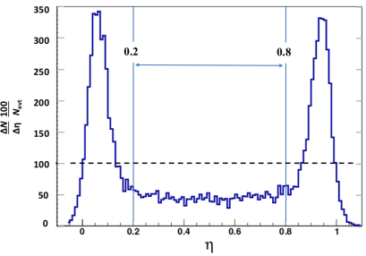
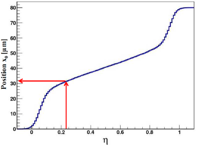
Fig. 4(a) shows the distribution of measured for the non-hadron-irradiated -stop sensor biased at 600 V after 0.2 days of source irradiation, which corresponds to a dose of 10 Gy. is the total number of events and the number of events in a bin of width . The value found in the central region is , which is significantly higher than the expected from the angular spread of mrad. To characterize charge sharing we use the quantity , where is the number of events in the interval , whilst 0.6 is the width of the interval. Thus gives the percentage of charge sharing relative to 100 % charge sharing.
In addition, allows the determination of , the distance of the traversing particle from the centre of strip , as discussed in Ref. [9]. The following is a brief summary of the derivation. Assuming a uniform distribution of events over the sensor with inter-strip spacing , the fraction of events in a given interval , , is equal to , where is the interval that corresponds to the selected interval. Thus the cumulative distribution normalized to pitch relates the measured value to the distance of the particle from strip . Fig. 4(b) shows an example of a measured relation.
The position resolution as a function of can be estimated using , where the uncertainty can be calculated from the signal-to-noise-ratio and the definition of . For a flat distribution between and 1 the relation is linear, and is independent of . We call this ideal charge division, if in addition most of the signal is induced in strips and .
4 Results
We first present results for the two non-hadron-irradiated sensors and then for the hadron-irradiated -stop sensor. An explanation and discussion of the observations with the aid of SYNOPSYS TCAD [10] simulations that include surface charges at the Si-SiO2 interface and different boundary conditions on the sensor surface are given in Sect. 5.
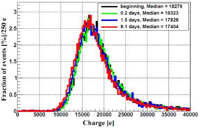
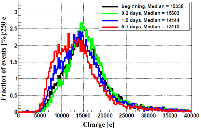
Fig. 5(a) shows the pulse-height distributions of the 4-strip clusters, PH(4-cluster), whilst Fig. 5(b) shows the corresponding pulse-height distributions for the seed clusters, PH(seed), for the non-hadron-irradiated -stop sensor fabricated on magnetic-Czochralski material, as measured 0, 0.2, 1.5 and 9.1 days after the start of irradiation with the source. The corresponding doses in the SiO2 are 0, 10, 75 and 450 Gy, respectively. For PH(4-cluster) we observe Landau distributions with dose-dependent changes of the median by and %, respectively. Significantly larger changes are observed for PH(seed): The median changes by and %, respectively. In addition, the shape of the PH(seed) distribution changes: The approximately triangular distribution with a maximum around 15 000 e changes to a distribution that is nearly flat between 7 500 and 15 000 e.
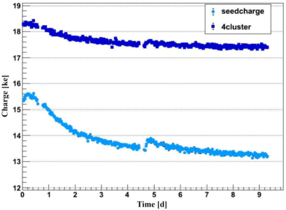
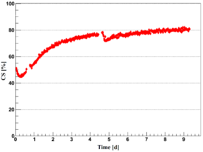
Fig. 6(a) shows the time dependence of the median of the PH(4-cluster) and PH(seed) distributions for the non-hadron-irradiated MCz -stop sensor biased at 600 V, whilst Fig. 6(b) shows the corresponding dependence of the charge sharing, . As a function of the measurement time, the dose in the SiO2 increases from 0 to about 450 Gy. For PH(4-cluster) we observe a constant value up to about 0.4 days, and then a steady decrease by about 5 %. For PH(seed) a much larger decrease by 15 % after an initial short term increase of 3 % is observed. is initially 52 %, 45 % after 0.3 days (15 Gy), and then steadily increases to 80 %. After 4.6 days the source was retracted, and a calibration of the electronics and a voltage scan for pedestal and noise determination between 0 and 1000 V was performed. This is seen as gaps and steps in the time dependencies.
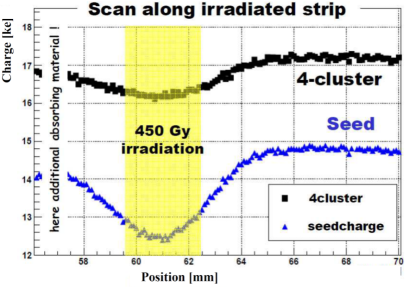
A source scan along the strips on which the source had been centred for 9.5 days is shown in Fig. 7. It is found that the decrease in PH(4-cluster) and in PH(seed) is limited to the region where the source had been positioned and that outside this region no effects of the irradiation are observed.
To investigate a possible dose-rate dependence, measurements were performed with a 38 MBq 90Sr source at a position that had not previously been exposed to the source. It is found that, within the accuracy of the measurements, the results only depend on dose and not on the dose-rate [2].
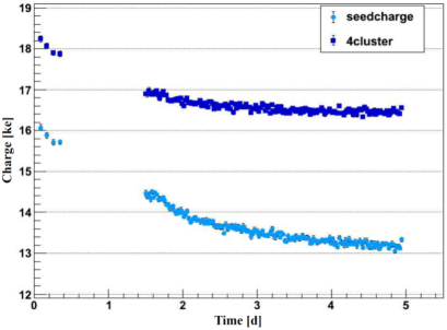
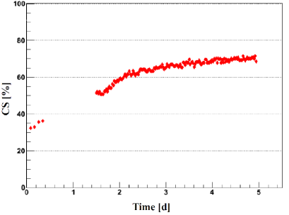
Fig. 8 shows the time dependence of the median values of PH(4-cluster) and PH(seed), and of measured for the non-hadron-irradiated -spray sensor built on float-zone silicon. Data between 0.4 and 1.4 days are missing, as during this time the nitrogen flow was interrupted and the sensor covered by an ice layer. Qualitatively the results are similar to those from the non-hadron-irradiated -stop sensor: The median of PH(4-cluster) decreases by about 10 %, PH(seed) by 20 %, and increases from 30 % to 70 %. We note the absence of the initial short time change observed for the -stop sensor.
| Annealing step | 1 | 2 | 3 | 4 | 5 | 6 |
|---|---|---|---|---|---|---|
| End time of annealing [d] | 23.4 | 24.7 | 25.7 | 27.0 | 28.1 | 30.5 |
| Duration of annealing [h] | 120 | 24 | 18 | 24 | 18 | 52 |
| SiO2 dose [Gy] before annealing | 780 | 790 | 810 | 820 | 830 | 850 |
| Temperature [∘C] | 20 | 40 | 60 | 80 | ||
| Bias voltage [V] during annealing | 600 | 600 | 600 | 600 | 350 | 600 |
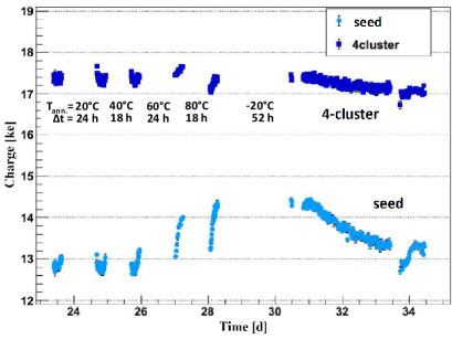
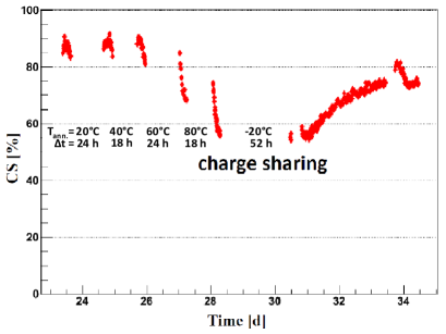
Next, the annealing behaviour was investigated for the -stop sensor fabricated using magnetic-Czochralski silicon after a dose of about 800 Gy from the source. Table 1 lists the individual annealing steps, and Fig. 9 shows the measured median values of PH(4-cluster), PH(seed) and . Only small changes are observed for PH(4-cluster): The largest change is a decrease by about 3 % after annealing at 80 ∘C, which quickly recovers after a few hours of exposure to the source. The changes for PH(seed) are larger: After every annealing step, PH(seed) is seen to have reached a value close to the one before annealing. During the typical 6 h of irradiation with the source immediately after the annealing, PH(seed) increases by for the annealing for 24 h at 60 ∘C, and for 18 h at 80 ∘C. Finally, during the 3 days of long-term measurements, PH(seed) decreases again and approaches the steady-state values shown in Fig. 6 at 9 days. The charge sharing also shows significant changes: After annealing, the value of has increased, however it decreases quickly when the sensor is irradiated again. After a long-term exposure of 3 days, the steady-state values shown in Fig. 6 at 9 days, are approached. It is clear that the observed behaviour is quite complex.
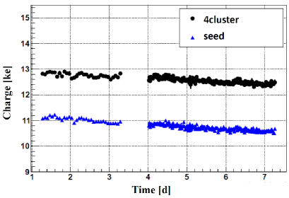
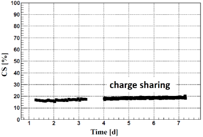
Finally, Fig. 10 gives results for the hadron-irradiated -stop sensor fabricated on float-zone silicon measured at C and a voltage of 1000 V: The median of PH(4-cluster) decreases by about 3 % after 7.5 days of irradiation, corresponding to a dose in the SiO2 of 375 Gy. The median of PH(seed) decreases by about 5 % and increases from 16 % to 19 %. We note that for the hadron-irradiated sensor the effects are significantly smaller than for the non-hadron-irradiated sensors.
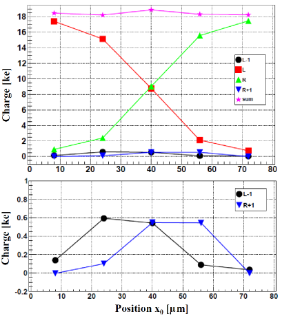
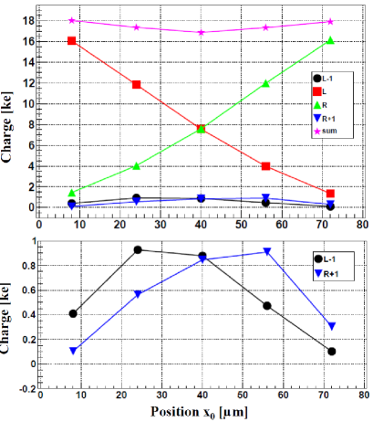
As discussed in Sect. 3, the measured value of allows the estimation of the distance, , of the particle passage from the centre of the readout strip and thus the investigation of the position dependence of the charge collection. Fig. 11 shows, for the non-hadron-irradiated -stop sensor fabricated on magnetic-Czochralski silicon biased at 600 V, the median values of PH(4-cluster), PH(-1), PH(), PH(), and PH(+1) as functions of for source dose values of 10 and 450 Gy. Comparing the distributions, it can be seen that for the 450 Gy data in the region between the readout strips, PH(4-cluster) decreases by about 12 %, and the pulses induced in strips -1 and +1 increase from about 3 % to 5 %. In Sect. 5 we will present a possible explanation of this observation.
5 Discussion of the results
Figs. 6 and 8 show that significant changes in the charge collection are already observed after 0.2 days, when the ionizing dose in the SiO2 at the maximum of the distribution is 10 Gy, and the NIEL is neq/cm2. Given such a low NIEL value, bulk damage is excluded as an explanation, and charge buildup in the insulators and surface damage have to be considered.
In SiO2 an average energy loss of eV is required to produce an pair [11, 12], resulting in a density of generated pairs of cm-3 Gy-1. Thus, for a SiO2 thickness of 1150 nm, a dose of 10 Gy generates cm pairs. A fraction of the pairs will annihilate on a time scale of picoseconds. As shown in Fig. 1.7 of Ref. [12] and in Ref. [13] this fraction depends on the ionization density and the local electric field: For 12 MeV electrons it is about 70 % at zero field, and 10 % at 1 MV/cm. The corresponding numbers for 10 keV X-rays are 90 % and 45 %, respectively. Electrons, thanks to their high mobility (approximately 20 cm2/(Vs) at room temperature) will leave the oxide. However holes, which have a mobility in the range to cm2/(Vs) at room temperature and even lower values at C, will charge up the oxide. As the electric field in the SiO2 points towards the Si, the holes will eventually reach the Si-SiO2 interface, where they either escape into the Si or are trapped as oxide charges.
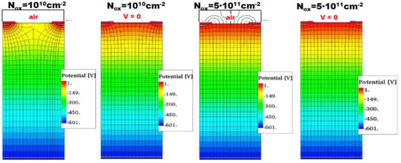
2-D simulations with SYNOPSYS TCAD [10] were made to calculate the electric field in the sensor for different oxide-charge densities, and boundary conditions on the sensor surface. The results are presented in Fig. 12, which shows the electric field stream lines and the electric potential for a sensor of thickness 200 m, bulk doping of cm-3 and a -spray dopant concentration of cm-2, at a bias voltage of 600 V. For the layout of the SiO2 and Si3N4 layers, and of the implants used in the simulations, we refer to Fig. 1(b). For the two simulations on the left side an oxide-charge density of cm-2 was assumed, and for the two simulations on the right side cm-2. Two different boundary conditions at the strip side were investigated: A potential of 0 V on a plane at 500 m distance from the sensor surface, and zero charge density on the sensor surface (denoted air), and a potential of 0 V on the sensor surface (denoted V ). The first boundary condition corresponds to the situation shortly after applying the voltage to the sensor, when the charge distribution on the sensor surface is the same as before applying the voltage. The second one corresponds to the equilibrium situation of the biased sensor, when surface charges have moved, until the longitudinal electric field on the surface vanishes. The time constant for reaching the equilibrium is a strong function of humidity and temperature, and can be as long as several days [14].
We note that for the simulation with cm-2, and in particular for the air boundary condition, most field stream lines originate at the readout strips. Thus for a particle at normal incidence, practically all generated electrons will reach a single readout strip, and apart from a small effect due to charge diffusion, there will be no charge division.
For the simulation with cm-2 the field distribution is very different, resembling the field of a pad diode. The reason is that the positive oxide-charge density, , is bigger than the negative charge density of the -spray doping, which results in an approximately constant potential at the Si-SiO2 interface. Therefore the electric-field component parallel to the interface is small, and electrons, which reach the Si-SiO2 interface within the typical charge collection time of a few nanoseconds, will drift to the readout strips on a much longer time scale. If this time scale is long compared to the integration time of the readout electronics, the electrons are effectively trapped at the Si-SiO2 interface, and signals will be recorded not only on strips and , but also on strips -1 and +1, and even beyond. This will be discussed in more detail below. Electronic cross-talk will also produce signals in strips -1 and +1. Simulations of the electric field in an sensor with -stop isolation for oxide-charge densities of and cm-2 are also reported in Ref. [15]. The results agree with our simulations; however the effects on charge collection had not been studied.
Fig. 11 shows that signals are actually observed in all four strips -1, , and +1 for particles passing between two readout strips. We also find that when the dose changes from 10 Gy to 450 Gy, the signals in the next-to-next-neighbour strips increase, and the cluster pulse height, PH(4-cluster), decreases. As the electronic cross-talk is the same in both cases, we conclude that the radiation from the source changes the electric field in the sensor, which causes the observed changes with radiation from the source.
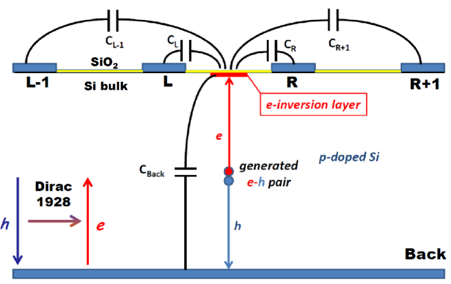
Signal formation in segmented sensors is usually described with the help of weighting fields [16, 17, 18], which describe the capacitative coupling of a charge at a given position in the sensor to the individual electrodes. For the following qualitative discussion we prefer the equivalent description in terms of effective coupling capacitors as presented in Ref. [19] and sketched in Fig. 13. It is more easily understood than the abstract weighting fields and allows an estimation of the cross-talk and the effect of the finite input capacitance of the readout electronics in a straightforward way.
For a charge positioned at the Si-SiO2 interface (e.g. at the head of the red arrow labeled in Fig. 13) we label the coupling capacitors between the position of the electron and the individual strips, , and the coupling capacitor to the backplane, . The figure is simplified, as it neither shows the capacitances between the readout strips, nor the capacitances of the coupling nor the finite effective input impedance of cables and readout electronics, which are responsible for cross-talk between readout channels. In the following discussion we assume that all electrodes are virtual grounds. This is a good approximation if the -coupling capacitances between the implants and the Al electrodes are large and the effective input impedance of the readout is small compared to the inter-strip and strip-to-backplane capacitances. Including inter-strip capacitances, coupling capacitances and finite input impedances for the readout is straightforward, but not necessary for the following discussion.
We first consider the case of a single pair generated somewhere in the sensor without charge trapping in the silicon crystal. In an sensor the holes drift to the back contact and the electrons towards the strip side, thereby inducing current transients in all electrodes. The charge induced in an electrode by a hole moving to the backplane, is equal to the charge induced by an electron moving from the backplane to the position where the hole was created. Thus, a hole from an pair moving to the backplane and the electron moving to the strip side, is equivalent to an electron moving all the way from the backplane to the strip side. As all electrodes are considered to be on virtual ground, an electron with charge that moves from the backplane to a readout strip induces in this strip and in the back electrode, a current transient whose integral is equal to . Currents are also induced in all other strips, but their integrals are zero. However, an electron trapped at the Si-SiO2 interface corresponds to charging up the capacitors , which are connected in parallel to the virtual ground, such that signals are induced in the electrodes . The cluster charge, which is the sum of all signals induced in the readout strips, is , and the charge loss is . If more than one pair is produced, the contributions from all pairs have to be added.
We can explain the increase of the charge losses with dose, seen at m in Fig. 11, with the formation of an inversion layer at the Si-SiO2 interface: The capacitance to the back plane, , is approximately proportional to the width of the inversion layer, whereas the capacitances of the inversion layer to the strips and depend only weakly on its width [20]. Thus, the wider the inversion layer, the larger the value of , and the bigger the charge losses. The reason for the increase with dose of the charges induced in the strips -1 and +1, seen in the bottom of Fig. 11, is not yet understood and needs further studies.
In the case described, where charge trapping occurs only at the Si-SiO2 interface, the signals induced in the readout strips do not depend on the position where the pairs were generated, but only on the position at which the electrons arrive at the strip side. If charge trapping in the silicon bulk occurs, which is the case for silicon sensors with significant bulk damage by hadrons, the situation is significantly more complicated and better treated using weighting fields. However, the calculation of weighting fields in bulk-damaged silicon sensors is quite complicated [21], and its use for sensors with significant bulk damage and charge trapping is far from obvious.
Hadron irradiation in silicon crystals produces defects with energy levels in the band gap. They cause generation currents and charge trapping. They also modify the electric field in the sensors [22]. For hadron fluences above typically neq/cm2 the defect densities exceed the initial doping concentration, and radiation damage effects become significant. The generation current in an sensor is dominated by holes at the back side and electrons at the strip side. Therefore, the fractions of occupied radiation-induced donors and acceptors vary with position, and the effective doping is strongly position dependent. Finally, the electric field in the sensor is the result of the interplay between the initial doping concentration, the additional effective doping from the charged radiation-induced defects, and the density of free charge carriers. We refer to Refs. [23, 24], where these effects have been discussed for the first time for silicon pad sensors. The high electron density in the region of the readout strips results in an electric field, which is qualitatively similar to the one shown in Fig. 12 left. This is our explanation for the low charge sharing and the reduced influence of the radiation-induced oxide-charge on the charge collection observed for the hadron-irradiated sensor and shown in Fig. 10. We note that the value for the hadron-irradiated sensor is close to the value expected from the angular distribution of the trigger electrons.
Next, we discuss the observation that the initial value and the initial dose-dependence of for the non-hadron-irradiated -stop and -spray sensor are different, as can be seen in Figs. 6(b) and 8(b). For the -stop sensor the initial value is about 50 % and initially decreases with dose, whereas for the -spray sensor it is about 30 % and increases. Our explanation is qualitative and should be confirmed using TCAD simulations. However, there is the problem that the parameters, which describe the buildup of oxide charges for high fields at the Si-SiO2 interface, are not known.
For the -spray sensor the negative space charge of the depleted -spray implant shields the positive oxide charge, whilst for the -stop sensor this shielding occurs only at the narrow -stop implants. Therefore more field lines will originate at the Si-SiO2 interface for the -stop sensor and the initial charge sharing will be larger. Our explanation for the initial difference in the change of the charge sharing is more speculative. The initial decrease of the charge sharing for the -stop sensor may be explained by the formation of a local electron inversion layer at the Si-SiO2 interface below the metal overhang. There, the electric field in the SiO2 is high and the recombination probability in the SiO2 is low, which leads to an accelerated buildup of oxide charges. Such a local inversion layer effectively extends the charge-collection region of the readout strips and thus reduces the charge sharing.
After about 4 days of irradiation with the source, which corresponds to a dose of about 200 Gy, saturates and the following values are reached: % for the -stop and % for the -spray sensor. We have not checked if the values become equal at higher surface doses, which one might naively expect.
We expect that the surface damage has opposite effects on the breakdown voltage for sensors and for sensors. For sensors, radiation-induced positive oxide charges compensate the negative charges of the doping, thus reducing the electric field below the metal overhang and at the corners of the implants. The breakdown voltage is therefore expected to increase with increasing surface damage. For sensors, the positive oxide charges add to the positive charges from the doping, which increases the electric field below the metal overhang and at the corner of the implants, leading to a decrease in breakdown voltage with increasing surface damage. Such a decrease has actually been observed and is documented in Refs. [2, 25, 26]. As shown in Refs. [27, 28], a special optimization of the sensor design can avoid this problem.
The annealing studies have only been made for the -stop sensor and the results are shown in Fig. 9. Significant effects have been found at annealing temperatures of 60 ∘C and 80 ∘C. After annealing increased by %, but during the following period of approximately 7 hours of irradiation with the source, it decreased again by %. After the different annealing steps the long-term measurement showed that the asymptotic value of , which is %, is again approached after about 4 days.
6 Summary and outlook
The measurements presented in this publication show that an ionizing dose as low as 10 Gy can cause significant changes in the charge collection and charge sharing of segmented silicon sensors. For a sensor with a -spray implant between the implants of the readout electrodes it is found that, once the positive oxide-charge density resulting from the ionizing radiation in the oxide exceeds the negative charge density of the depleted implants, the field in the sensor is similar to the field in a pad diode. In addition, electron-inversion layers can form at the Si-SiO2 interface if the positive oxide-charge density is sufficiently high. Under these conditions some charge losses and approximately ideal charge division between the two readout strips adjacent to the particle passage were observed. The results for sensors with -stop implants were qualitatively similar. As the radiation-induced positive oxide-charge density saturates for doses above kGy at a value of a few cm-2 [1], we expect that for -spray dopant concentrations exceeding these values, no significant changes with dose in charge sharing and charge losses due to surface damage will occur. For a hadron-irradiated sensor the observed changes with ionizing dose were significantly smaller than for the non-hadron-irradiated sensors. Qualitative and sometimes speculative explanations are given, which are based on simplified TCAD simulations of the electric field in the sensor. For a quantitative understanding more detailed TCAD simulations will be required. However, precise information on surface radiation damage, the charging up of the insulators, high-field charge injection into insulators, and on the boundary conditions on the sensor surface, is presently not available. Last but not least, the study shows the importance of taking both bulk and surface damage into account when designing silicon sensors for low- and high-radiation environments.
The impact of changes in charge sharing and charge losses on the performance of silicon detectors with high spatial resolution depends very much on the type and performance of the readout electronics used. For analogue readout with a good signal-to-noise-ratio, , charge sharing can be used to optimize the spatial resolution, which is then given by the product of pitch and . However, if the is poor and a relatively high readout threshold has to be set, it will be difficult to reach a high detection efficiency. As shown in this paper for a strip sensor with 80 m pitch, the pulse height of the seed strip is frequently smaller than 50 % of the most probable value (mpv) of the cluster pulse-height distribution. To reach high efficiencies, the pulse-height threshold has to be below mpv. If a pulse-height threshold of 3 times the variance of the noise is required to limit the number of noise hits, a value for the cluster signal of at least 7.5 is required. If binary readout is used, the threshold requires a careful optimization with respect to noise hits, efficiency, cluster size and position resolution. We conclude that it is important to take charge sharing properly into account when optimizing segmented silicon sensors.
Acknowledgements
The research leading to these results has received funding from the European Commission under the FP7 Research Infrastructures project AIDA, grant agreement no. 262025. The information herein only reflects the views of its authors and not those of the European Commission and no warranty expressed or implied is made with regard to such information or its use.
The authors thank W. Gärtner and the workshop of the Institute for Experimental Physics for designing and constructing the setup, and P. Buhmann, R.-P. Feller, M. Matysek and R. Mohrmann for the continuous improvement and maintenance of the measurement infrastructure of the detector laboratory as well as for helping with the measurements. We are also grateful to the HGF Alliance Physics at the Terascale, which has partially funded the setup used for the measurements, and to the BMBF, the Ministry of Research and Education of the German Federal Republic, for funding the PhD position of J. Erfle within the Forschungsschwerpunkt FSP-102, Elementarteilchenphysik mit dem CMS-Experiment.
7 References
References
- [1] J. Zhang, I. Pintilie, E. Fretwurst, R. Klanner, H. Perrey, and J. Schwandt, Study of radiation damage induced by 12 keV X-rays in MOS structures built on high-resistivity n-type silicon, Journal of Synchrotron Radiation 19 (3): 340346, 2012.
- [2] J. Erfle, Irradiation study of different silicon detectors for the CMS tracker upgrade, PhD thesis, University of Hamburg, DESY-THESIS-2014-010, 2014.
- [3] C. Henkel, Charge losses in silicon strip sensors after in-situ irradiation with a source, BSc thesis, University of Hamburg, 2014, unpublished.
- [4] R. Klanner et al., for the CMS Tracker Collaboration, Impact of low-dose electron irradiation on n+p silicon strip sensors, POS (TIPP 2014).
- [5] A. Dierlamm for the CMS Tracker Collaboration, Characterisation of silicon sensor materials and designs for the CMS Tracker Upgrade, PoS (Vertex 2012) 016.
- [6] R. Marco-Hernandez, A portable readout system for microstrip silicon sensors, Nuclear Instruments and Methods in Physics Research A 623(1): 207209, 2010, and IEEE Transactions on Nuclear Science 56(3): 16421649, 2009.
- [7] S. Müller, The Beam Condition Monitor 2 and the Radiation Environment of the CMS Detector at the LHC, Note: CMS-TS-2010-042 (2010).
- [8] I. Dawson, Radiation background simulation and verification at the LHC: Examples from the ATLAS experiment and its upgrades, PoS (Vertex 2012) 015.
- [9] E. Belau, et al., Charge collection in silicon strip detectors, Nuclear Instruments and Methods in Physics Research 214(2-3): 253260, 1983.
- [10] Synopsys TCAD webpage: http://www.synopsys.com.
- [11] T.P. Ma and P.V. Dressendorfer, Ionization Effects in MOS Devices and Circuits, John Wiley & Sons, New York, 1989.
- [12] T.R. Oldham, Ionization Radiation Effects in MOS Oxides, World Scientific Publishing Co. Pte. Ltd., Singapore, 1999.
- [13] J. Zhang, Radiation damage studies and design of a silicon pixel sensor for science at the XFEL, PhD thesis, University of Hamburg, DESY-THESIS-2013-018.
- [14] T. Poehlsen, et al., Charge losses in segmeted silicon sensors at the SiSiO2 interface, Nuclear Instruments and Methods in Physics Research A 700(1): 2239, 2013.
- [15] Y. Unno, et al., Evaluation of test structures for the novel n+-in-p pixel and strip sensors for very high radiation environments, Nuclear Instruments and Methods in Physics Research A 731(1): 183188, 2013.
- [16] W. Shockley, Currents to conductors induced by a moving point charge, Journal of Applied Physics 9 635636, 1938.
- [17] S. Ramo, Currents induced by electron motion, Proceedings of the I.R.E. 27(9) 584585, 1939.
- [18] J.B. Gunn, A general expression for electrostatic induction and its application to semiconductor devices, Solid-State Electronics 7(10) 739742, 1964.
- [19] U. Koetz, et al., Silicon strip detectors with capacitive charge division, Nuclear Instruments and Methods in Physics Research A 235: 481487, 1985.
- [20] P.W. Cattaneo, Capacitances in micro-strip detectors: A conformal mapping approach, Solid-State Electronics 54(3) 252258, 2010.
- [21] L.-A. Hamel and M. Julien, Generalized demonstration of Ramo’s theorem with space charge and polarization effects, Nuclear Instruments and Methods in Physics Research A 597: 207215, 2008.
- [22] G. Lindström, Radiation damage in silicon detectors, Nuclear Instruments and Methods in Physics Research A 512: 3043, 2003.
- [23] D. Menichelli, M. Bruzzi, Z. Li, and V. Eremin, Modelling of observed double-junction effect, Nuclear Instruments and Methods in Physics Research A 426: 135139, 1999.
- [24] V. Eremin, E. Verbitskaya and Z. Li, The origin of double peak electric field distribution in heavily irradiated silicon detectors, Nuclear Instruments and Methods in Physics Research A 476: 556564, 2002.
- [25] T. Ohsugi, et al., Micro-discharge noise and radiation damage of silicon microstrip sensors, Nuclear Instruments and Methods in Physics Research A 383: 166173, 1996.
- [26] J. Schwandt, E. Fretwurst, R. Klanner, I. Pintilie, and J. Zhang, Study of high-dose X-ray radiation damage in silicon sensors, Proceedings of SPIE, vol. 8777, p. 87770K, 2013.
- [27] J. Schwandt, E. Fretwurst, R. Klanner, I. Kopsalis, and J. Zhang, Design and First Tests of a Radiation-Hard Pixel Sensor for the European X-Ray Free-Electron Laser, IEEE Transactions on Nuclear Science 61(4): 18941901, 2014.
- [28] J. Schwandt, Design of a Radiation-Hard Pixel Sensor for X-Ray Science, PhD thesis, University of Hamburg, DESY-THESIS-2014-029.
8 Appendix: Author list
W. Adam, T. Bergauer, M. Dragicevic, M. Friedl, R. Fruehwirth, M. Hoch, J. Hrubec, M. Krammer, W. Treberspurg, W. Waltenberger
Institut für Hochenergiephysik der Österreichischen Akademie der Wissenschaften (HEPHY), Vienna, Austria
S. Alderweireldt, W. Beaumont, X. Janssen, S. Luyckx, P. Van Mechelen, N. Van Remortel, A. Van Spilbeeck
Universiteit Antwerpen, Belgium
P. Barria, C. Caillol, B. Clerbaux, G. De Lentdecker, D. Dobur, L. Favart, A. Grebenyuk, Th. Lenzi, A. Léonard, Th. Maerschalk, A. Mohammadi, L. Perniè, A. Randle-Conde, T. Reis, T. Seva, L. Thomas, C. Vander Velde, P. Vanlaer, J. Wang, F. Zenoni
Brussels-ULB, Belgium
S. Abu Zeid, F. Blekman, I. De Bruyn, J. D’Hondt, N. Daci, K. Deroover, N. Heracleous, J. Keaveney, S. Lowette, L. Moreels, A. Olbrechts, Q. Python, S. Tavernier, P. Van Mulders, G. Van Onsem, I. Van Parijs, D.A. Strom
Brussels-VUB, Belgium
S. Basegmez, G. Bruno, R. Castello, A. Caudron, L. Ceard, B. De Callatay, C. Delaere, T. Du Pree, L. Forthomme, A. Giammanco, J. Hollar, P. Jez, D. Michotte, C. Nuttens, L. Perrini, D. Pagano, L. Quertenmont, M. Selvaggi, M. Vidal Marono
CP3/IRMP - Université catholique de Louvain - Louvain-la-Neuve – Belgium
N. Beliy, T. Caebergs, E. Daubie, G.H. Hammad
University of Mons, Belgium
J. Härkönen, T. Lampén, P. -R. Luukka, T. Mäenpää, T. Peltola, E. Tuominen, E. Tuovinen
Helsinki Institute of Physics, Finland
P. Eerola
University of Helsinki and Helsinki Institute of Physics, Finland
T. Tuuva
Lappeenranta University of Technology, Lappeenranta, Finland
G. Beaulieu, G. Boudoul, C. Combaret, D. Contardo, G. Gallbit, N. Lumb, H. Mathez, L. Mirabito, S. Perries, D. Sabes, M. Vander Donckt, P. Verdier, S. Viret, Y. Zoccarato
Université de Lyon, Université Claude Bernard Lyon 1, CNRS/IN2P3, Institut de Physique Nucléaire de Lyon, France
J.-L. Agram, E. Conte, J.-Ch. Fontaine
Groupe de Recherches en Physique des Hautes Energies, Université de Haute Alsace, Mulhouse, France
J. Andrea, D. Bloch, C. Bonnin, J.-M. Brom, E. Chabert, L. Charles, Ch. Goetzmann, L. Gross, J. Hosselet, C. Mathieu, M. Richer, K. Skovpen
Institut Pluridisciplinaire Hubert Curien, Université de Strasbourg, IN2P3-CNRS, Strasbourg, France
C. Autermann, M. Edelhoff, H. Esser, L. Feld, W. Karpinski, K. Klein, M. Lipinski, A. Ostapchuk, G. Pierschel, M. Preuten, F. Raupach, J. Sammet, S. Schael, G. Schwering, B. Wittmer, M. Wlochal, V. Zhukov
I. Physikalisches Institut, RWTH Aachen University, Germany
C. Pistone, G. Fluegge, A. Kuensken, M. Geisler, O. Pooth, A. Stahl
III. Physikalisches Institut, RWTH Aachen University, Germany
N. Bartosik, J. Behr, A. Burgmeier, L. Calligaris, G. Dolinska, G. Eckerlin, D. Eckstein, T. Eichhorn, G. Fluke, J. Garay Garcia, A. Gizhko, K. Hansen, A. Harb, J. Hauk, A. Kalogeropoulos, C. Kleinwort, I. Korol, W. Lange, W. Lohmann, R. Mankel, H. Maser, G. Mittag, C. Muhl, A. Mussgiller, A. Nayak, E. Ntomari, H. Perrey, D. Pitzl, M. Schroeder, C. Seitz, S. Spannagel, A. Zuber
DESY, Hamburg, Germany
H. Biskop, V. Blobel, P. Buhmann, M. Centis-Vignali, A.-R. Draeger, J. Erfle, E. Garutti, J. Haller, Ch. Henkel, M. Hoffmann, A. Junkes, R. Klanner, T. Lapsien, S. Mättig, M. Matysek, A. Perieanu, J. Poehlsen, T. Poehlsen, Ch. Scharf, P. Schleper, A. Schmidt, J. Schwandt, V. Sola, G. Steinbrück, B. Vormwald, J. Wellhausen
University of Hamburg, Germany
T. Barvich, Ch. Barth, F. Boegelspacher, W. De Boer, E. Butz, M. Casele, F. Colombo, A. Dierlamm, R. Eber, B. Freund, F. Hartmann222 Also at CERN, Th. Hauth, S. Heindl, K.-H. Hoffmann, U. Husemann, A. Kornmeyer, S. Mallows, Th. Muller, A. Nuernberg, M. Printz, H. J. Simonis, P. Steck, M. Weber, Th. Weiler
Karlsruhe-IEKP, Germany
A. Bhardwaj, A. Kumar, A. Kumar, K. Ranjan
Department of Physics and Astrophysics, University of Delhi, Delhu, India
H. Bakhshiansohl, H. Behnamian, M. Khakzad, M. Naseri
Institute for Research in Fundamental Sciences (IPM), Tehran, Iran
P. Cariola, G. De Robertis, L. Fiore, M. Franco, F. Loddo, G. Sala, L. Silvestris
INFN Bari, Italy
D. Creanza, M. De Palma, G. Maggi, S. My, G. Selvaggi
INFN and Dipartimento Interateneo di Fisica, Bari, Italy
S. Albergo, G. Cappello, M. Chiorboli, S. Costa, F. Giordano, A. Di Mattia, R. Potenza, M.A. Saizu333 Also at Horia Hulubei National Institute of Physics and Nuclear Engineering (IFIN-HH), Bucharest, Romania, A. Tricomi, C. Tuvè
INFN and University of CATANIA, Italy
G. Barbagli, M. Brianzi, R. Ciaranfi, C. Civinini, E. Gallo, M. Meschini, S. Paoletti,
G. Sguazzoni
INFN Firenze, Italy
V. Ciulli, R. D’Alessandro, S. Gonzi, V. Gori, E. Focardi, P. Lenzi, E. Scarlini, A. Tropiano, L. Viliani
INFN and University of Firenze, Italy
F. Ferro, E. Robutti
INFN Genova, Italy
M. Lo Vetere
INFN and University of Genova, Italy
S. Gennai, S. Malvezzi, D. Menasce, L. Moroni, D. Pedrini
INFN Milano-Bicocca, Italy
M. Dinardo, S. Fiorendi, R.A. Manzoni
INFN and Universita degli Studi di Milano-Bicocca, Italy
P. Azzi, N. Bacchetta
INFN Padova, Italy
D. Bisello, M. Dall’Osso, T. Dorigo, P. Giubilato, N. Pozzobon, M. Tosi, A. Zucchetta
INFN and University of Padova, Italy
F. De Canio, L. Gaioni, M. Manghisoni, B. Nodari, V. Re, G. Traversi
INFN Pavia and University of Bergamo, Italy
D. Comotti, L. Ratti
INFN Pavia and University of Pavia, Italy
G. M. Bilei, L. Bissi, B. Checcucci, D. Magalotti444 Also at Modena and Reggio Emilia University, Italy, M. Menichelli, A. Saha, L. Servoli, L. Storchi
INFN Perugia, Italy
M. Biasini, E. Conti, D. Ciangottini, L. Fanò, P. Lariccia, G. Mantovani, D. Passeri, P. Placidi, M. Salvatore, A. Santocchia, L.A. Solestizi, A. Spiezia
INFN and University of Perugia, Italy
N. Demaria, A. Rivetti
INFN Torino, Italy
R. Bellan, S. Casasso, M. Costa, R. Covarelli, E. Migliore, E. Monteil, M. Musich, L. Pacher, F. Ravera, A. Romero, A. Solano, P. Trapani
INFN and University of Torino, Italy
R. Jaramillo Echeverria, M. Fernandez, G. Gomez, D. Moya, F.J. Gonzalez Sanchez, F.J. Munoz Sanchez, I. Vila, A.L. Virto
Instituto de Fısica de Cantabria (IFCA), CSIC-Universidad de Cantabria, Santander, Spain
D. Abbaneo, I. Ahmed, E. Albert, G. Auzinger, G. Berruti, G. Bianchi, G. Blanchot,
H. Breuker, D. Ceresa, J. Christiansen, K. Cichy, J. Daguin, M. D’Alfonso, A. D’Auria, S. Detraz, S. De Visscher, D. Deyrail, F. Faccio, D. Felici, N. Frank, K. Gill, D. Giordano, P. Harris, A. Honma, J. Kaplon, A. Kornmayer, M. Kortelainen, L. Kottelat, M. Kovacs, M. Mannelli, A. Marchioro, S. Marconi, S. Martina, S. Mersi, S. Michelis, M. Moll, A. Onnela, T. Pakulski, S. Pavis, A. Peisert, J.-F. Pernot, P. Petagna, G. Petrucciani, H. Postema, P. Rose, M. Rzonca, M. Stoye, P. Tropea, J. Troska, A. Tsirou, F. Vasey, P. Vichoudis, B. Verlaat, L. Zwalinski
European Organization for Nuclear Research (CERN), Geneva, Switzerland
F. Bachmair, R. Becker, L. Bäni, D. di Calafiori, B. Casal, L. Djambazov, M. Donega, M. Dünser, P. Eller, C. Grab, D. Hits, U. Horisberger, J. Hoss, G. Kasieczka, W. Lustermann, B. Mangano, M. Marionneau, P. Martinez Ruiz del Arbol, M. Masciovecchio, L. Perrozzi, U. Roeser, M. Rossini, A. Starodumov, M. Takahashi, R. Wallny
ETH Zürich, Zürich, Switzerland
C. Amsler555 Now at University of Bern, Switzerland, K. Bösiger, L. Caminada, F. Canelli, V. Chiochia, A. de Cosa, C. Galloni, T. Hreus, B. Kilminster, C. Lange, R. Maier, J. Ngadiuba, D. Pinna, P. Robmann, S. Taroni, Y. Yang
University of Zürich, Switzerland
W. Bertl, K. Deiters, W. Erdmann, R. Horisberger, H.-C. Kaestli, D. Kotlinski, U. Langenegger, B. Meier, T. Rohe, S. Streuli
Paul Scherrer Institut, Villigen, Switzerland
P.-H. Chen, C. Dietz, U. Grundler, W.-S. Hou, R.-S. Lu, M. Moya, R. Wilken
National Taiwan University, Taiwan, ROC
D. Cussans, H. Flacher, J. Goldstein, M. Grimes, J. Jacob, S. Seif El Nasr-Storey
University of Bristol, Bristol, United Kingdom
J. Cole, P. Hobson, D. Leggat, I. D. Reid, L. Teodorescu
Brunel University, Uxbridge, United Kingdom
R. Bainbridge, P. Dauncey, J. Fulcher, G. Hall, A.-M. Magnan, M. Pesaresi, D.M. Raymond, K. Uchida
Imperial College, London, United Kingdom
J.A. Coughlan, K. Harder, J. Ilic, I.R. Tomalin
STFC, Rutherford Appleton Laboratory, Chilton, Didcot, United Kingdom
A. Garabedian, U. Heintz, M. Narain, J. Nelson, S. Sagir, T. Speer, J. Swanson, D. Tersegno, J. Watson-Daniels
Brown University, Providence, Rhode Island, USA
M. Chertok, J. Conway, R. Conway, C. Flores, R. Lander, D. Pellett, F. Ricci-Tam,M. Squires, J. Thomson, R. Yohay
University of California, Davis, California, USA
K. Burt, J. Ellison, G. Hanson, M. Malberti, M. Olmedo
University of California, Riverside, California, USA
G. Cerati, V. Sharma, A. Vartak, A. Yagil, G. Zevi Della Porta
University of California, San Diego, California, USA
V. Dutta, L. Gouskos, J. Incandela, S. Kyre, N. McColl, S. Mullin, D. White
University of California, Santa Barbara, California, USA
J. P. Cumalat, W. T. Ford, A. Gaz, M. Krohn, K. Stenson, S.R. Wagner
University of Colorado, Boulder, Colorado, USA
B. Baldin, G. Bolla, K. Burkett, J. Butler, H. Cheung, J. Chramowicz, D. Christian, W.E. Cooper, G. Deptuch, G. Derylo, C. Gingu, S. Gruenendahl, S. Hasegawa, J. Hoff, J. Howell, M. Hrycyk, S. Jindariani, M. Johnson, A. Jung, U. Joshi, F. Kahlid, C. M. Lei, R. Lipton, T. Liu, S. Los, M. Matulik, P. Merkel, S. Nahn, A. Prosser, R. Rivera, A. Shenai, L. Spiegel, N. Tran, L. Uplegger, E. Voirin, H. Yin
Fermi National Accelerator Laboratory (FNAL), Batavia, Illinois, USA
M.R. Adams, D.R. Berry, A. Evdokimov, O. Evdokimov, C.E. Gerber, D.J. Hofman, B.K. Kapustka, C. O’Brien, D.I. Sandoval Gonzalez, H. Trauger, P. Turner
University of Illinois, Chicago, Illinois, USA
N. Parashar, J. Stupak, III
Purdue University Calumet, Hammond, Indiana, USA
D. Bortoletto, M. Bubna, N. Hinton, M. Jones, D.H. Miller, X. Shi
Purdue University, West Lafayette, Indiana, USA
P. Tan
University of Iowa, Iowa City, Iowa, USA
P. Baringer, A. Bean, G. Benelli, J. Gray, D. Majumder, D. Noonan, S. Sanders, R. Stringer
University of Kansas, Lawrence, Kansas, USA
A. Ivanov, M. Makouski, N. Skhirtladze, R. Taylor
Kansas State University, Manhattan, Kansas, USA
I. Anderson, D. Fehling, A. Gritsan, P. Maksimovic, C. Martin, K. Nash, M. Osherson, M. Swartz, M. Xiao
Johns Hopkins University, Baltimore, Maryland, USA
Massachusetts Institute of Technology, Cambridge, Massachusetts, USA
J.G. Acosta, L.M. Cremaldi, S. Oliveros, L. Perera, D. Summers
University of Mississippi, Mississippi, USA
K. Bloom, S. Bose, D.R. Claes, A. Dominguez, C. Fangmeier, R. Gonzalez Suarez, F. Meier, J. Monroy
University of Nebraska, Lincoln, Nebraska, USA
K. Hahn, S. Sevova, K. Sung, M. Trovato
Northwestern University, Evanston, Illinois, USA
E. Bartz, D. Duggan, E. Halkiadakis, A. Lath, M. Park, S. Schnetzer, R. Stone, M. Walker
Rutgers University, Piscataway, New Jersey, USA
S. Malik, H. Mendez, J.E. Ramirez Vargas
University of Puerto Rico, Mayaguez, Puerto Rico, USA
M. Alyari, J. Dolen, J. George, A. Godshalk, I. Iashvili, J. Kaisen, A. Kharchilava, A. Kumar, S. Rappoccio
State University of New York, Buffalo, New York, USA
J. Alexander, J. Chaves, J. Chu, S. Dittmer, G. Kaufman, N. Mirman, A. Ryd, E. Salvati, L. Skinnari, J. Thom, J. Thompson, J. Tucker, L. Winstrom
Cornell University, Ithaca, New York, USA
B. Akgün, K.M. Ecklund, T. Nussbaum, J. Zabel
Rice University, Houston, Texas, USA
B. Betchart, R. Covarelli, R. Demina, O. Hindrichs, G. Petrillo
University of Rochester, New York, USA
R. Eusebi, I. Osipenkov, A. Perloff, K.A. Ulmer
Texas A&M University, College Station, Texas, USA
A. G. Delannoy, P. D’Angelo, W. Johns
Vanderbilt University, Nashville, Tennessee, USA