On Asymptotic Gate Complexity and Depth of Reversible Circuits With Additional Memory
Abstract
The reversible logic can be used in various research areas, e. g. quantum computation, cryptography and signal processing. In the paper we study reversible logic circuits with additional inputs, which consist of NOT, CNOT and C2NOT gates. We consider a set of all transformations that can be realized by reversible circuits with inputs. An analogue of Lupanov’s method for the synthesis of reversible logic circuits with additional inputs is described. We prove upper asymptotic bounds for the Shannon gate complexity function and the depth function in case of : if and if .
keywords:
Reversible logic, gate complexity, circuit depth, asymptotic bounds.dmitriy.zakablukov@gmail.com \submitted19 March 2016 \titleheadGate Complexity and Depth of Reversible Logic {subject} 03D15 Complexity of computation.
1 Introduction
The reversible logic is essential in the quantum computing. It also has a great potential in designing various computing devices with low power consumption. [Landauer (1961)] proved that the irreversibility of computations leads to the energy dissipation regardless of the underlying technology. [Bennett (1973)] showed that the absence of heat generation can be achieved only when a circuit is completely built from reversible gates. The main problem is that we should find a compromise between the gate complexity, the depth (working time) of a reversible circuit and the amount of used memory (additional inputs) when solving the problem of reversible logic synthesis. Unfortunately, strict asymptotic bounds for the gate complexity and the depth of reversible circuits haven’t been found so far, especially in the case of using additional inputs.
The circuit complexity theory goes back to the work of [Shannon (1949)]. He was the first who suggested to consider the complexity of the minimal switching circuit, which realizes a Boolean function, as a complexity measure of this function. For today, the asymptotic gate complexity of a Boolean function of variables in the basis of classical gates “NOT, OR, AND” is well-known.
The problem of computations with the limited memory was considered by [Karpova (1987)]. She proved that the asymptotic gate complexity of a circuit, which consists of the gates corresponding to all Boolean functions of variables and which uses at least three memory registers, depends on the value of , but doesn’t depend on the number of used memory registers. Also she proved that any Boolean function can be realized in such a circuit using only two memory registers.
[Lupanov (1970)] considered circuits of functional elements with delays. He proved that in a regular basis of functional elements any Boolean function can be realized in a circuit with asymptotically the best gate complexity and with the delay , where is the constant depending on the basis. Though the depth and the delay of a circuit can be defined differently (see Khrapchenko 1995), in the model of reversible circuit described below we can consider the value of as the circuit depth. However a dependency of on the number of used memory registers was not considered for the “classical” circuits.
A gate is called reversible if it implements a bijective transformation. There are several known reversible gates for today. Among them are the NOT gate; the controlled NOT (CNOT) gate, introduced by Feynman (1985); the Toffoli gate (C2NOT) introduced by Toffoli (1980); the Fredkin gate, etc.
A set of all transformations that can be implemented by reversible circuits with inputs was considered in Zakablukov (2015). Also the Shannon gate complexity function and the depth function as functions of and the number of additional inputs (additional memory) were defined and upper bounded in the case, when additional inputs are not allowed in a reversible circuit.
The subject of this paper is reversible logic circuits, which consist of NOT, CNOT and C2NOT gates and which can use an unlimited amount of additional inputs (unlike the reversible circuits we have studied earlier, see Zakablukov 2015).
We will describe an analogue of Lupanov’s method for synthesizing a reversible circuit with additional inputs, which has the minimal gate complexity or the minimal depth. Using this synthesis approach, we will prove the following upper asymptotic bounds for the functions and :
Also, some upper bounds for the quantum weight function will be proved.
Using the lower and upper bounds for the functions and , we state that the usage of additional memory in a reversible circuit, which consists of NOT, CNOT and C2NOT gates, almost always allows to reduce its gate complexity and the depth.
2 Background
The controlled NOT gate (CNOT) was introduced by Feynman (1985). The Toffoli gate was introduced by Toffoli (1980). The generalized Toffoli gate with multiple control inputs is usually denoted as CkNOT or TOFk+1, where stands for the number of control inputs. The synthesis of reversible circuits consisting of these gates was discussed in several works, see Zakablukov (2014); Khlopotine et al. (2002); Miller & Dueck (2003); Miller et al. (2003); Saeedi et al. (2007); Maslov et al. (2007); Saeedi et al. (2010).
We use the following notation for a generalized Toffoli gate.
Definition 2.1.
A generalized Toffoli gate with control inputs is a reversible gate with inputs, which defines a transformation as follows:
where is a set of indices of control input lines and is an index of a controlled output line, .
From the definition one can note that a gate TOF(a) is a NOT gate, TOF(a,b) is a CNOT gate and TOF(a,b,c) is a C2NOT gate.
We denote a set of all TOF gates, , as (i. e. all NOT, CNOT and C2NOT gates). An upper and/or a lower indices in TOF will be omitted, if their value is clear from the context.
Fan-in, fan-out and a random connection of inputs and outputs of gates in a reversible circuit are forbidden. We assume that all gates in a reversible circuit have exactly numbered inputs and outputs and that the -th output of a gate is connected only to the -th input of the following gate. Thus in our model of a reversible circuit a graph associated with a circuit presents itself a single chain. We will refer to such a connection of reversible gates as composition.
A symbol from a set can be assigned to the -th input and output of a gate. All these symbols can be treated as names of memory registers (indices of memory cells), which store the current computation result of a circuit.
If we consider all the gates from regardless of an underlying technology, we can assume that they all have the same technological cost. However, in a quantum technology, for example, a technological cost of NOT and CNOT gates is much less than a technological cost of a Toffoli gate (see Barenco et al. 1995). Hence, we will assume that a gate from has the weight depending on the underlying technology. More precisely, we will asume that all NOT and CNOT gates from have the same weight and all C2NOT gates from have the weight .
Let a reversible circuit with inputs be a composition of gates from : . In the paper we study the following circuit’s properties:
-
1.
The gate complexity , equal to the number of gates .
-
2.
The quantum weight , equal to the sum of weights of all its gates.
-
3.
The depth , equal to the number of gates in the path from inputs to outputs that cannot be executed simultaneously.
Note that the quantum weight of a reversible circuit is not equal to its technological cost, because they may significantly differ. But we can state that in most cases a greater value of the function means a greater technological cost of a reversible circuit .
A formal definition of the reversible circuit depth for our circuit model can be found in Zakablukov (2015). Here we just want to remind that a reversible circuit has the depth , if for every two of its gates and the following equation holds:
Also, the depth of a reversible circuit equals to the minimal number of disjoint sub-circuits with the depth of each equal to one in the following equation:
For example, a reversible circuit (see 1) has the gate complexity and the depth , because we can divide the circuit into three disjoint sub-circuits with the depth of each equal to one in the following manner: .
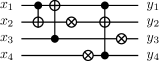
Note that the reversible circuit is equivalent to another one with the depth equal to three: . Therefore from here on we will consider that such circuits are different in terms of our reversible circuit’s model, but equivalent in terms of the equality of Boolean transformations defined by them.
3 Asymptotic bounds for reversible circuits without additional inputs
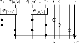
It is well-known that a reversible circuit with inputs defines an even permutation on the set , see Shende et al. (2003). But it can also implement a transformation , where , with or without an additional memory. A circuit with inputs implements a transformation , if there is such a permutation for circuit outputs that every input of the form is transformed by the circuit into an output after applying the permutation , where (see 2).

We remind that in our terminology expressions “implements a transformation” and “defines a transformation” have different meanings. If a circuit implements a transformation and has exactly inputs, we will say that this circuit implements without additional inputs.
We marked all “don’t care” outputs of a reversible circuit by the symbol * on 2. In most cases these outputs will not be cleared out in the end, i. e. they will contain a computational garbage. Unfortunately, this garbage can be removed only if a transformation implemented by a reversible circuit is bijective. In this case we can clear out all garbage outputs, except ones corresponding to the inputs of , with the help of a part of the existing circuit (let’s denote it as ). Then we can append a reversible circuit implementing the transformation with generating of computational garbage and with clearing out the outputs corresponding to the inputs of . And finally, we can remove this generated garbage with the help of a part of the circuit (let’s denote it as ). Thus a resulting circuit will have the gate complexity and the depth (see 3).

Therefore, all asymptotic bounds for the gate complexity and the depth will be given later for a reversible circuit with a computational garbage on the outputs. To obtain similar bounds for a reversible circuit without a computational garbage on the outputs, one should multiply them by four.
Let be the set of all transformations and be the set of all transformations, which can be implemented by reversible circuits with inputs. It is not difficult to show that , , is equal to the set of transformations that are defined by all the permutations from the alternating group and if .
We denote the minimum gate complexity, the minimum depth and the minimum quantum weight of a reversible circuit among all reversible circuits implementing a transformation with additional inputs as , and respectively. The Shannon gate complexity function , the depth function and the quantum weight function are defined as follows:
For the purpose of estimating the function , we will count the number of NOT/CNOT and C2NOT gates in a reversible circuit separately. If we denote the number of NOT and CNOT gates in a reversible circuit as and the number of C2NOT gates as , then the following equation holds:
| (1) |
We proved (see Zakablukov 2015) that there is such that for the following equations hold:
| (2) | ||||
| (3) | ||||
| (4) |
Also, the following uppper bounds for a reversible circuit without additional inputs were proved (see Zakablukov 2015):
| (5) | ||||
| (6) | ||||
| (7) |
where is an arbitrarily slowly growing function and
Unfortunately, there are no known upper asymptotic bounds for the functions , and in the case when a reversible circuit can use an unlimited amount of additional inputs for today. Nevertheless, it has been already showed that in some cases the usage of additional memory in a reversible circuit consisting of gates from allows to reduce its gate complexity and the depth, see Barenco et al. (1995); Miller et al. (2010); Abdessaied et al. (2013).
4 Reducing the gate complexity with the help of additional inputs
Lupanov described asymptotically the best synthesis algorithm of a Boolean function in the basis . He proved that any Boolean function of variables can be implemented in a circuit with the gate complexity and with the total delay no more than , see Lupanov (1970). We will modify Lupanov’s method in order to synthesize a reversible circuit, which consists of gates from and implements a transformation with additional inputs.
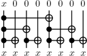
The basis is functionally complete, therefore it can be used to implement any transformation . Let’s express every element of this basis via a composition of NOT, CNOT and C2NOT gates (see 4). As we can see, this requires no more than two gates and one additional input for every element of the basis.

First, we prove the following lemma about the gate complexity of a reversible circuit implementing all conjunctions of variables of the form , .
Lemma 4.1.
All conjunctions of variables of the form , , can be implemented in a reversible circuit , which consists of gates from , with the gate complexity and with additional inputs.
Proof 4.2.
First step is obtaining inversions of all input variables: , . This can be done using NOT and CNOT gates and additional inputs.
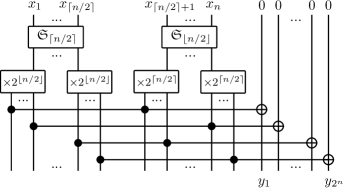
We construct our reversible circuit this way: using circuits and , we implement all conjunctions of the first and the last variables (see 5). After this we implement conjunctions of outputs of the circuit with outputs of the circuit . This can be done using C2NOT gates and additional inputs.
Hence, the following equation holds:
Now we can prove the first theorem of the paper.
Theorem 4.3.
where and are arbitrarily slowly growing functions.
Proof 4.4.
We will describe a new synthesis algorithm A1, which is similar to the Lupanov’s method and whose main goal is the reduction of the gate complexity with the help of additional inputs.
Let’s consider a transformation . It can be represented as follows:
| (8) |
Each of Boolean transformations
where , is a Boolean transformation and can be represented as the system of coordinate functions , , .
The value of every coordinate function can be calculated with the help of an analogue of a disjunctive normal form:
| (9) |
All conjunctions of the form can be divided into the groups with no more than conjunctions in each. The number of such groups is . Using conjunctions of a single group, we can construct no more than Boolean functions by the formula (9).
Let be the set of all Boolean functions that can be constructed with the help of conjunctions of an -th group, . Then . Therefore, we can rewrite equation (9) as follows:
| (10) |
Note that all Boolean functions of a group can be implemented, using a similar technique as in the 4.1. From the 5 we can see that all C2NOT gates will be simply replaced by compositions of two CNOT gates. Thus, CNOT gates and additional inputs are required for this part in total.
The synthesis algorithm A1 constructs a reversible circuit implementing the transformation (8) from the following sub-circuits (see 6):

-
1.
Sub-circuit implementing all conjunctions of the first variables by the 4.1 with the gate complexity and with additional inputs. The sub-circuit almost completely consists of C2NOT gates (the number of other gates is negligible).
-
2.
Sub-circuit implementing all Boolean functions for all by the formula (9) with the gate complexity and with additional inputs (see the note above about the implementation of all Boolean functions of a group ). The sub-circuit consists only of CNOT gates.
-
3.
Sub-circuit implementing all coordinate functions , , , by the formula (10) with the gate complexity and with additional inputs. The sub-circuit consists only of CNOT gates.
-
4.
Sub-circuit implementing all conjunctions of the last variables by the 4.1 with the gate complexity and with additional inputs. The sub-circuit almost completely consists of C2NOT gates (the number of other gates is negligible).
-
5.
Sub-circuit implementing the transformation by the formula (8) with the gate complexity and with additional inputs. The sub-circuit consists only of C2NOT gates.
We are seeking the values of parameters and that satisfy the following conditions:
In this case and . This implies that for any growing function the values of parameters and will satisfy the conditions above.
Summing up gate complexities and the number of additional inputs of sub-circuits –, we obtain the following bounds:
Hence, if and , where and are growing functions, the following equations hold:
Since the synthesis algorithm A1 can produce a reversible circuit for any Boolean transformation , we can state that , if , where and are arbitrarily slowly growing functions.
Theorem 4.5.
where and are arbitrarily slowly growing functions.
Now we can upper bound the quantum weight of a reversible circuit with additional inputs.
Theorem 4.7.
where and are arbitrarily slowly growing functions.
Proof 4.8.
To prove the bound of the theorem, we should count the number of NOT, CNOT and C2NOT gates in a reversible circuit produced by the synthesis algorithm A1.
From the description of the algorithm we can see that
Providing and , where and are growing functions, we obtain the following upper bounds:
From these upper bounds and the equation (1) the upper bound for the function from the theorem follows.
Note that in the case, when , the following equation holds:
where ; and are arbitrarily slowly growing functions. In other words, the number of C2NOT gates in a reversible circuit produced by the synthesis algorithm A1 is negligible compared to the overall gate complexity. And from the equations (2), (4), (5) and (7) it follows that in a reversible circuit without additional inputs the number of C2NOT gates is equivalent by the order of magnitude to the overall gate complexity.
5 Reducing the depth with the help of additional inputs
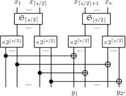
We described the synthesis algorithm A1, whose main goal was the gate complexity reduction with the help of additional inputs. However, we can use a similar technique to reduce the depth of a reversible circuit. Let’s denote such an algorithm as A2. The essence of the synthesis algorithm A2 is the copying of the value from an output to the additional inputs with the logarithmic depth (see 7). After this we can perform a desired operation with the depth equal to one. All we need to do is to copy the value a sufficient number of times.
First, we prove the following lemma about the depth of a reversible circuit implementing all conjunctions of variables of the form , .
Lemma 5.1.
All conjunctions of variables of the form , , can be implemented in a reversible circuit , which consists of gates from , with the depth , the gate complexity and with additional inputs.
Proof 5.2.
First step is obtaining inversions of all input variables: , . This can be done with the depth , using NOT and CNOT gates and additional inputs.
We construct our reversible circuit in the same way as in 4.1, using sub-circuits and (see 8). Any output of these sub-circuits will be used no more than in conjunctions, so all conjunctions can be implemented with the depth , using CNOT gates, C2NOT gates and additional inputs.
Hence, the following equations hold:
Now we can prove the next theorem of the paper.
Theorem 5.3.
A reversible circuit with the depth has the gate complexity and the quantum weight , where and are arbitrarily slowly growing functions.
Proof 5.4.
We will describe the synthesis algorithm A2, which is similar to the synthesis algorithm A1 and whose main goal is the reduction of the depth with the help of additional inputs.
Note that all Boolean functions of a group can be implemented, using a similar technique as in the 5.1. This requires CNOT gates ( gates are used to copy values to the additional inputs) and additional inputs (see 9).
The synthesis algorithm A2 constructs a reversible circuit implementing the transformation (8) from the following sub-circuits (see 10):

-
1.
Sub-circuit implementing all conjunctions of the first variables by the 5.1 with the depth , the gate complexity and with additional inputs. The sub-circuit contains C2NOT gates.
-
2.
Sub-circuit implementing all Boolean functions for all by the formula (9) with the depth , the gate complexity and with additional inputs (see the note above about the implementation of all Boolean functions of a group ). The sub-circuit consists only of CNOT gates.
-
3.
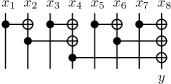
Sub-circuit implementing all coordinate functions , , , by the formula (10). The feature of this sub-circuit is that a Boolean function can be used more than once. The maximum usage count for a function is . So, first of all we need to copy the values from outputs of the sub-circuit for all such Boolean functions. This can be done with the depth equal to , using no more than gates and additional inputs (see 7). After this, we implement XOR function of obtained outputs with the depth equal to , the gate complexity equal to and without additional inputs (see 11). Therefore, the sub-circuit has the depth , the gate complexity and additional inputs. It consists only of CNOT gates.
-
4.
Sub-circuit implementing all conjunctions of the last variables by the 5.1 with the depth , the gate complexity and with additional inputs. The sub-circuit contains C2NOT gates.
-
5.
Sub-circuit , which is needed to copy times every output of the sub-circuit . This can be done with the depth , the gate complexity and with additional inputs. The sub-circuit consists only of CNOT gates.
-
6.
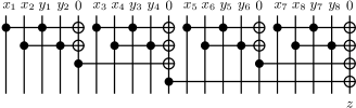
Sub-circuit implementing the transformation by the formula (8). The structure of the sub-circuit is as follows: all coordinate functions are grouped by functions ( groups in total, which correspond to outputs of the transformation ). Functions in a group are again grouped by two. For every pair of functions we implement a conjunction of the corresponding outputs of sub-circuits and , using 2 C2NOT gates and one additional input for storing an intermediate result (see 12). Thus, this part of the sub-circuit has the depth equal to 2, requires C2NOT gates and additional inputs. After this, in every of groups of obtained outputs we implement XOR function with the logarithmic depth (see 11 and 12). This part of the sub-circuit has the depth equal to , requires CNOT gates and doesn’t require additional inputs, because we can use the existing outputs.
Summing up, the sub-circuit has the depth , the gate complexity and additional inputs.
Note that the sub-circuits – and – can work in parallel, because they use disjoint subsets of the inputs .
We are seeking the values of parameters and that satisfy the following conditions:
In this case .
Summing up depths, gate complexities and the number of additional inputs for all sub-circuits –, we obtain the following bounds for the circuit parameters.
The depth:
| (11) |
The gate complexity:
| (12) |
The number of additional inputs:
| (13) |
From the description of the synthesis algorithm A2 we can see that
This implies that
| (14) | ||||
| (15) |
Let , where is a growing function. In this case and
We can choose any arbitrarily slowly growing functions and .
Hence, we obtain the following bounds for the circuit parameters:
Since the synthesis algorithm A2 can produce a reversible circuit for any Boolean transformation , we can state that , if .
Also we can state that and , where and are arbitrarily slowly growing functions.
Finally, we prove the last theorem of the paper.
Theorem 5.5.
where is an arbitrarily slowly growing function. A reversible circuit with the depth has the gate complexity and the quantum weight .
Proof 5.6.
Proof is based on the proof of the previous theorem.
Let , where is a growing function. In this case and
We can see that we always able to choose a growing function for any growing function .
Since the synthesis algorithm A2 can produce a reversible circuit for any Boolean transformation , we can state that , if , where is an arbitrarily slowly growing function.
Also, and .
6 Conclusion
We have discussed the problem of the general synthesis of a reversible circuit, which consists of NOT, CNOT and C2NOT gates and which has additional inputs, with the lowest possible gate complexity and depth. We have studied the Shannon gate complexity function , the depth function and the quantum weight function for a reversible circuit with additional inputs, which implements a transformation from the set .
The main result of the paper is the following claim.
Claim 1.
The usage of additional memory in a reversible circuit consisting of NOT, CNOT and C2NOT gates almost always allows to reduce its gate complexity, the depth and the quantum weight.
Solving the problem of the reversible logic synthesis, one should find a compromise between the gate complexity, the depth (working time) and the amount of used memory (additional inputs) of a reversible circuit. Unfortunately, we were not able to establish good upper and lower bounds for the depth function , which would be asymptotically equivalent to each other by the order of magnitude. However, the obtained bounds are sufficient to prove the main claim of the paper.
Further research should establish more precise relationship of a reversible circuit’s parameters from the number of additional inputs in the circuit. We hope that the paper will be the first step in this direction.
The reported study was partially supported by RFBR, research project No. 16-01-00196 A.
References
- Abdessaied et al. (2013) Nabila Abdessaied, Robert Wille, Mathias Soeken & Rolf Drechsler (2013). Reducing the Depth of Quantum Circuits Using Additional Circuit Lines. In Reversible Computation, GerhardW. Dueck & D.Michael Miller, editors, volume 7948 of Lecture Notes in Computer Science, 221–233. Springer Berlin Heidelberg. ISBN 978-3-642-38985-6.
- Barenco et al. (1995) Adriano Barenco, Charles H. Bennett, Richard Cleve, David P. DiVincenzo, Norman Margolus, Peter Shor, Tycho Sleator, John A. Smolin & Harald Weinfurter (1995). Elementary gates for quantum computation. Phys. Rev. A 52(5), 3457–3467.
- Bennett (1973) C. H. Bennett (1973). Logical Reversibility of Computation. IBM Journal of Research and Development 17(6), 525–532. ISSN 0018-8646.
- Feynman (1985) Richard P. Feynman (1985). Quantum Mechanical Computers. Optics News 11(2), 11–20.
- Karpova (1987) N. A. Karpova (1987). On Complexity of Computations with Limited Memory. In FCT, Lothar Budach, Rais Gatic Bakharajev & Oleg Borisovic Lipanov, editors, volume 278 of Lecture Notes in Computer Science, 234–235. Springer. ISBN 3-540-18740-5.
- Khlopotine et al. (2002) Andrei B. Khlopotine, Marek A. Perkowski & Pawel Kerntopf (2002). Reversible Logic Synthesis by Iterative Compositions. In IWLS, 261–266.
- Khrapchenko (1995) V. M. Khrapchenko (1995). New inequality relations between depth and delay. Diskr. Mat. 7(4), 77–85. In Russian.
- Landauer (1961) R. Landauer (1961). Irreversibility and Heat Generation in the Computing Process. IBM Journal of Research and Development 5(3), 183–191. ISSN 0018-8646.
- Lupanov (1970) O. B. Lupanov (1970). On Circuits of Functional Elements with Delays. In Probl. Kibernet., volume 23, 43–81. Nauka Publishers, Moscow. In Russian.
- Maslov et al. (2007) D. A. Maslov, G. W. Dueck & D. M. Miller (2007). Techniques for the Synthesis of Reversible Toffoli Networks. ACM Trans. Des. Autom. Electron. Syst. 12(4). ISSN 1084–4309.
- Miller & Dueck (2003) D. M. Miller & G. W. Dueck (2003). Spectral Techniques for Reversible Logic Synthesis. In 6th International Symposium on Representations and Methodology of Future Computing Technologies, 56–62.
- Miller et al. (2010) D. M. Miller, R. Wille & R. Drechsler (2010). Reducing Reversible Circuit Cost by Adding Lines. In Multiple-Valued Logic (ISMVL), 2010 40th IEEE International Symposium on, 217–222. ISSN 0195-623X.
- Miller et al. (2003) D. Michael Miller, Dmitri A Maslov & Gerhard W. Dueck (2003). A Transformation Based Algorithm for Reversible Logic Synthesis. In Proceedings of the 40th Annual Design Automation Conference, DAC ’03, 318–323. ACM, New York, NY, USA. ISBN 1-58113-688-9.
- Saeedi et al. (2007) M. Saeedi, M. Sedighi & M. S. Zamani (2007). A novel synthesis algorithm for reversible circuits. In Computer-Aided Design, 2007. ICCAD 2007. IEEE/ACM International Conference on, 65–68. ISSN 1092-3152.
- Saeedi et al. (2010) Mehdi Saeedi, Morteza Saheb Zamani, Mehdi Sedighi & Zahra Sasanian (2010). Reversible Circuit Synthesis Using a Cycle-based Approach. J. Emerg. Technol. Comput. Syst. 6(4), 13:1–13:26. ISSN 1550-4832.
- Shannon (1949) Claude E. Shannon (1949). The Synthesis of Two Terminal Switching Circuits. Bell System Technical Journal 28(1), 59–98. ISSN 0005-8580.
- Shende et al. (2003) V. V. Shende, A. K. Prasad, I. L. Markov & J. P. Hayes (2003). Synthesis of reversible logic circuits. Computer-Aided Design of Integrated Circuits and Systems, IEEE Transactions on 22(6), 710–722. ISSN 0278-0070.
- Toffoli (1980) Tommaso Toffoli (1980). Reversible computing. In Automata, Languages and Programming, Jaco de Bakker & Jan van Leeuwen, editors, volume 85 of Lecture Notes in Computer Science, 632–644. Springer Berlin Heidelberg.
- Zakablukov (2014) Dmitry V. Zakablukov (2014). Fast Synthesis of Invertible Circuits Based on Permutation Group Theory. Prikl. Diskr. Mat. 24(2), 101–109. In Russian.
- Zakablukov (2015) Dmitry V. Zakablukov (2015). On Asymptotic Gate Complexity and Depth of Reversible Circuits Without Additional Memory. ArXiv e-prints URL http://arxiv.org/abs/1504.06876.