Electronic properties of bilayer graphenes strongly coupled to interlayer stacking and an external electric field
Abstract
Bilayer graphene (BLG) with a tunable bandgap appears interesting as an alternative to graphene for practical applications, thus its transport properties are being actively pursued. Using density functional theory and perturbation analysis, we investigated, under an external electric field, the electronic properties of BLGs in various stackings relevant to recently observed complex structures. We established the first phase diagram summarizing the stacking-dependent gap openings of BLGs for a given field. We further identified high-density midgap states, localized on grain boundaries, even under a strong field, which can considerably reduce overall transport gap.
pacs:
61.48.Gh, 73.22.Pr, 73.21.AcThe discovery of graphene has opened new avenues for studying the role of dimensionality on the fundamental properties of materials Novoselov . Although graphene shows excellent electrical properties Bolotin , the zero bandgap of graphene limits its practical application as an electronic device. On the other hand, gap opening is possible in BLG, thus making it a very promising material that overcomes graphene’s key limitation while retaining many of its interesting properties. For example, massive Dirac fermions in BLG exhibit a bandgap tunable by applying a transverse electric field (E-field) MinMcCann2 ; this has been demonstrated by optical OhtaMakZhang and electrical transport measurements using dual-gated devices Tay ; OostingaVelascoVarlet . However, these measurements leave a couple of unsolved problems: 1) the origin of unexpectedly small transport gaps that are two orders of magnitude smaller than optical gaps Tay and 2) the origin of anomalous low-temperature ( 2 K) transport behaviors dominated by hopping between localized midgap states, presumably induced from disorders or defects Tay ; Tanabe .
Recent experiments have revealed complex configurations in BLG, including various stacking domains induced by rotational faults and soliton formation Lin ; Alden ; Hibino . While AB stacking is energetically most favorable, the non-AB-stacking region can be stabilized by a minute twist Kim and the stacking boundary Lin . The local stacking configuration is strongly coupled to its electronic structure and its response to an external E-field. Therefore, it is critically important, fundamentally and practically, to understand the observed complex stackings and their impact on the overall electronic properties.
In this letter, using the framework of an effective Hamiltonian based on density functional theory (DFT) and perturbation theory, we analyze gap-opening properties of BLGs near the high-symmetry stackings (AA, AA′, and AB), under an applied E-field. We establish a phase diagram for the stacking-dependent gap openings, and further identify grain boundaries containing non-AB stackings as a source for high-density midgap states even under a strong E-field. Our findings offer insight to understanding the intrinsic transport properties of BLGs.
Our DFT calculations adopt the Perdew-Burke-Ernzerhof version of exchange-correlation functional Perdew and the projector augmented wave method Kresse1 for ionic potentials as implemented in the Vienna Ab Initio Simulation Package Kresse2 . We obtain interlayer distances between 3.25 Å (AB) and 3.45 Å (AA) with van der Waals correction Tkatchenko ; interlayer distance of all the configurations is fixed at 3.35 Å (unless specified) with practically no changes in their band structures. To ensure an accurate bandgap, the 2D DFT band structure near the point is interpolated Waninter using maximally localized Wannier functions MarzariSouza . Effective Hamiltonians are constructed with the obtained hopping parameters truncated to the first nearest interlayer hoppings (see details in Supplemental Materials).
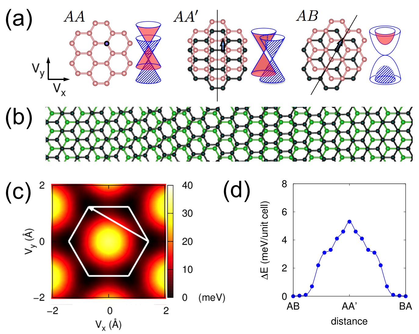
One of the intriguing properties of BLG is that a change in weak interlayer interaction (which is an order of magnitude smaller than the intralayer coupling strength) accompanied by a modification in stacking configuration can significantly alter the electronic structure around the Fermi level. Figure 1(a) illustrates schematic band structures of AA, AA′, and AB stacking, where we define systems with equivalent two sublattices, such as AA and AA′, as sublattice-symmetric systems; otherwise, they are sublattice-asymmetric stackings (such as AB).
Figure 1(b) shows the atomistic modeling of an experimentally observed domain boundary Alden . Here, for visual clarity, we made the phase boundary region (the region of continuous structural transition between two AB-stacking regions) much smaller than the experimental ones. Figure 1(c) plots stacking-dependent potential energy with optimized interlayer distances in the 2D translation vector space, where AB stacking is used as a reference point. The arrow denotes the displacement vector between the left and right domains in Fig. 1(b). Local stacking configurations of the transition region are distributed on this arrow. To remove this soliton-like boundary, one needs to displace the one on the left or right domain by a displacement vector. The minimum energy path between the two AB stackings lies along the edge of the hexagon with an energy barrier of 5.3 meV/cell (see Fig. 1(d)). Though this energy barrier seems quite small, the stacking domain should move as a whole so that the high energy barrier, which is proportional to the area of the domain ( unit cell), should be overcome. This explains the observed stability of non-AB stacking regions.
The gap-opening mechanism of BLGs can be highly stacking dependent. Thus, we first examine the individual band structures near the high-symmetry stackings. We then discuss the gap-opening properties across complex domain boundaries. Their effective Hamiltonian in crystal momentum () space can be described by a 4 4 matrix with the basis , , , and , where and represent sublattice indices and the subscripts and denote the upper and lower graphene layer, respectively. Here, the 2 2 block-diagonal components correspond to the individual graphene layers while all others describe interlayer coupling. We will now focus only on the effective Hamiltonian near the points; band structures around can be obtained by applying time-reversal symmetry to those of .
First we consider the configurations of AA stacking. Neglecting small Bloch phase variations under the Fourier transformations of interlayer coupling, we find that the Hamiltonian of AA stacking around becomes
| (1) |
with defined as
| (2) |
where the Fermi velocity multiplied by the reduced Planck constant becomes eVÅ and . ( eV) is obtained by the Fourier transformation of the interlayer hopping between () and (), FT . The hopping parameters between () and () become zero because the Bloch phases of three interlayer nearest neighbors cancel each other at the point; that is, .
By changing our basis to the bonding and antibonding state of each sublattice, the decoupling of two Dirac cones becomes more transparent as follows:
| (3) |
which is a block-diagonal Hamiltonian describing two Dirac cones with energy shift as shown in the schematic band diagram of Fig. 1(a).
In the AA′-stacking configuration, one can also explicitly illustrate the decoupling of Dirac cones by changing the basis to interlayer bonding and antibonding of phase-shifted sublattices []. The Hamiltonian of AA′ stacking then becomes
| (4) |
where eV and eV, corresponding to two Dirac cones separated by 0.22 eV in energy with an additional 0.08 Å-1 splitting in -space. Wavefunctions of the decoupled Dirac cones of both AA and AA′ stackings have interlayer antibonding and bonding characteristics, depicted respectively in red (shaded) and blue (hatched) in Fig. 1(a).
The Hamiltonian of AB staking can be written as
| (5) |
that is, there are doubly degenerate states at the Fermi level composed of one sublattice per layer, with no direct coupling between them. In this case two Dirac points are merged at the point and split into bonding, antibonding, and nonbonding types (see Fig. 1(a)).
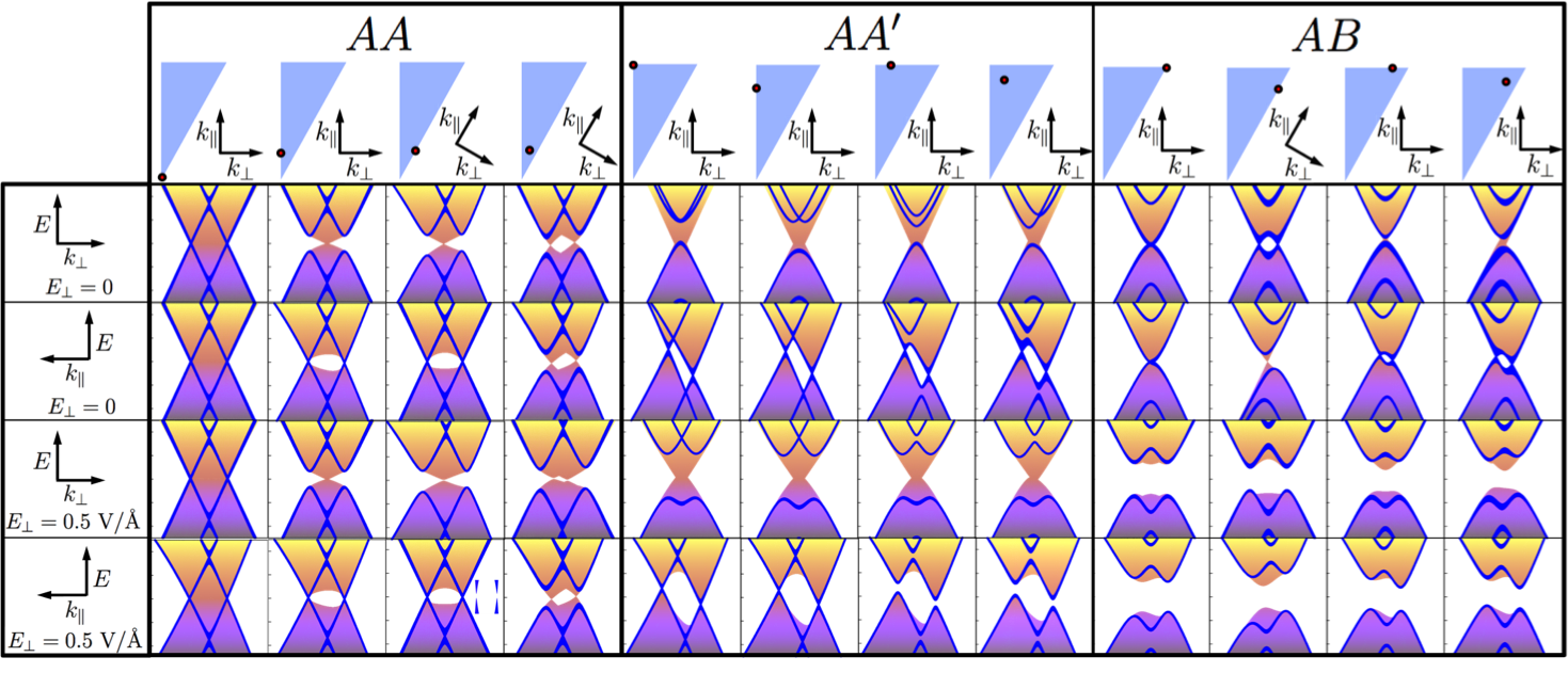
Next, we trace how a small translation or an external E-field can change the band structures, especially near the Fermi level. Our approach is to treat small translations and E-fields as perturbations to the individual high-symmetry stackings.
The AA panel of Fig. 2 summarizes projected (onto and ) band structures for around-AA-stacked graphenes without and with an E-field. Since interlayer hopping parameters ( and ) are the same, one cannot generate an onsite energy difference in the 2 2 diagonal block simply by atomic translation, which excludes the direct coupling between two crossing bands (i.e., no gap opening). At the Fermi level, the hole band of one Dirac cone is degenerated along with the electron band of the other Dirac cone. The Fermi surface of the AA stacking is the intersection of two vertically (energetically) shifted cones, a circle. A small translation results in a slight -shift and a coupling of two Dirac cones; a -shift changes the circular intersection into a tilted ellipse (which is still a circle when projected on -space), while a coupling introduces energy splitting at the intersection. In general, the energy splitting depends on the angular position of the intersection and becomes zero at two points. These form two crossing points near the Fermi level as shown in the second row. An applied E-field introduces an additional energy splitting that also depends on the angular position and becomes zero at two points. When an E-field is combined with a sublattice-symmetric translation, their zero splitting points coincide and the system remains metallic. In contrast, with the sublattice-asymmetric translation, each zero coupling points are at a different position and the crossing points disappear as shown in the inset in the fourth row. Especially, when sublattice-asymmetric translation is applied toward AB stacking in the presence of a reflection and time-reversal symmetry, the minimum bandgaps occur along and are located exactly at the same energy. This means that the critical field for opening a gap is infinitesimally small. The perturbational results on the size of the bandgap are summarized in Table 1. As an example, the fourth row in the AA block of Fig. 2 shows a small bandgap of 10 meV (see the inset) for an asymmetric translation of 0.3 Å and an E-field of 0.5 eV/Å.
| reference | AA | AA′ | AB |
| translation | toward AB | toward AB | any direction |
| direction | |||
| (pseudo-) gap | |||
| parameters | eVÅ | eV | |
| Å-2 | (eV/Å) | ||
| eV | eV | ||
| ( V/Å) | 0.15 eV | 0.52 eV | 0.55 eV |
Changes in band structures for around-AA′ stacking are well pronounced in the plane [the blues lines in the second and fourth rows of the AA′ block in Fig. 2]. Of the four bands in that plane, only different Dirac cones can be coupled by a translation. In contrast, under sublattice-symmetric translation, only parallel-band pairs of each Dirac cone are coupled, resulting in a balanced repulsion between them. On the other hand, under sublattice-asymmetric translation only non-parallel-band pairs of each cone are coupled, which induces an unfavorable crossing. Also in this slice, E-field only couples parallel-band pairs for sublattice-symmetric translation. Though the crossing point in a Dirac cone does not open, each Dirac cone’s crossing band now has a small component of the opposite Dirac cone. If we apply an E-field with sublattice-symmetric stacking, crossing bands still remain crossed because in a Dirac cone, one crossing band does not have a component parallel to the other crossing band. But if an E-field is applied to sublattice-asymmetric stacking, each crossing band now has a small component parallel to the other crossing bands, which opens a small bandgap. In spite of Dirac cones opening, the energy level of each Dirac point is different [the fourth row in the AA′ block of Fig. 2], thus a relatively strong E-field is required to change this pseudogap into a true gap.
Finally, we move on to the properties of around-AB stacking. As the stacking deviates from exact AB, the doubly degenerate states of AB at the point immediately split into two crossing points. This feature is demonstrated in the second and third columns of the AB block in Fig. 2. From a symmetry viewpoint, the threefold rotational symmetry of monolayer graphene is recovered in AA- and AB-stacked BLG. Combined with translational symmetry, this imposes a threefold symmetry around the point. Because two separated crossing points are not compatible with the symmetry, wavefunction symmetries change during the merging of two crossing points. It was reported that this merging process is very sensitive to miniscule translation (0.01 Å) and the band topology near the Fermi level changes Son . Around AB stacking, an E-field opens a bandgap. Especially, from the eigenvalues of the Hamiltonian, the bandgap is , where eV. All the perturbational results for the bandgap are summarized in Table 1.
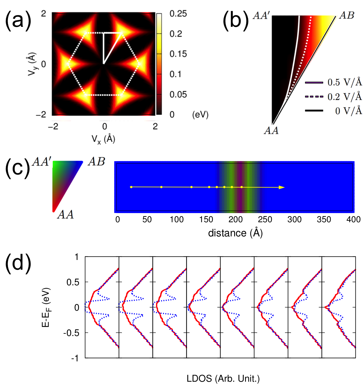
Figure 3(a) presents the stacking-dependent bandgap under a perpendicular E-field of 0.5 V/Å. A sizable bandgap opens only around the AB stacking while the rest still remains metallic. As E-field goes to zero, the metal-semiconductor phase boundary approaches the line connecting AA and AB stacking, and the entire region becomes metallic as shown in Fig. 3(b). Though no bandgap opens by a pure translation, a minute bandgap (7 meV) was reported Shallcross for a specific rotation angle without any E-field. To investigate the effect of the non-AB stacking region on the transport property, we constructed an atomic model of a stacking domain boundary with a transition length of 50 Å (Fig. 3 (c)). Tight-binding parameters are assigned to each atom according to its local stacking configuration TBassign . When 0.5 eV of onsite energy difference between two layers is applied, which corresponds to 0.5 V/Å of E-field, a bandgap opens at the AB stacking region while there remains finite density of states at the non-AB stacking region (Fig. 3(d)). This indicates that a high density of midgap states is localized along stacking boundaries even under a strong E-field. Because the apparent transport gap is actually estimated from the activation energy of the carrier, a conduction through these midgap states can explain the small transport gap and the low-temperature hopping transport in dual-gated devices.
In summary, we theoretically investigated stacking-dependent gap-opening properties of symmetry-broken bilayer graphenes, and established a bandgap phase diagram. Our findings may prove to be instrumental in developing graphene-based electronic devices.
Acknowledgments
This research was supported by the Center for Nanophase Materials Sciences, Oak Ridge National Laboratory by the Scientific User Facilities Division, Office of Basic Energy Sciences, U.S. Department of Energy. J. R., S. H., and G. K. were supported by (1) the Nano∙Material Technology Development Program (2012M3A7B4049888) through the NRF, funded by the Ministry of Science, ICT and Future Planning; (2) the Priority Research Center Program (2010-0020207); and (3) the Basic Science Research Program (2013R1A2009131) through NRF, funded by the Ministry of Education in Korea.
References
- (1) K. S. Novoselov, D. Jiang, F. Schedin, T. J. Booth, V. V. Khotkevich, S. V. Morozov, and A. K. Geim,, Proc. Nat. Acad. Sci. 102, 10451 (2005).
- (2) K. I. Bolotin, K. J. Sikes, Z. Jiang, M. Klima, G. Fudenberg, J. Hone, P. Kim, and H. L. Stormer, Solid State Commun. 146, 351 (2008).
- (3) H. K. Min, B. Sahu, S. K. Banerjee, and A. H. MacDonald, Phys. Rev. B 75, 155115 (2007); E. McCann, Phys. Rev. B 74, 161403(R) (2006).
- (4) T. Ohta, A. Bostwick, T. Seyller, K. Horn, and E. Rotenberg, Science 313, 951 (2006); K. F. Mak, C. H. Lui, J. Shan, and T. F. Heinz, Phys. Rev. Lett. 102, 256405 (2009); Y. B. Zhang, T. T. Tang, C. Girit, Z. Hao, M. C. Martin, A. Zettl, M. F. Crommie, Y. R. Shen, and F. Wang, Nature (London) 459, 820 (2009).
- (5) T. Taychatanapat and P. Jarillo-Herrero, Phys. Rev. Lett. 105, 166601 (2010).
- (6) J. B. Oostinga, H. B. Heersche, X. Liu, A. F. Morpurgo, and L. M. Vandersypen, Nature Mater. 7, 151 (2008); T. Taychatanapat and P. Jarillo-Herrero, Phys. Rev. Lett. 105, 166601 (2010); J. Velasco Jr, Y. Lee, Z. Zhao, L. Jing, P. Kratz, M. Bockrath, and C. N. Lau, Nature Nanotechnol. 7, 156 (2012); A. Varlet, M. H. Liu, V. Krueckl, D. Bischoff, P. Simonet, K. Watanabe, T. Taniguchi, K. Richter, K. Ensslin, and T. Ihn, Phys. Rev. Lett. 113, 116601 (2014).
- (7) S. Tanabe, Y. Sekine, H. Kageshima, M. Nagase, and H. Hibino, Jpn. J. Appl. Phys. 50, 04DN04 (2011).
- (8) J. Lin, W. Fang, W. Zhou, A. R. Lupini, J. C. Idrobo, J. Kong, S. J. Pennycook, and S. T. Pantelides, Nano Lett. 13, 3262 (2013).
- (9) J. S. Alden, A. W. Tsen, P. Y. Huang, R. Hovden, L. Brown, J. Park, D. A. Muller, and P. L. McEuen, Proc. Nat. Acad. Sci. USA 110, 11256 (2013).
- (10) H. Hibino, S. Mizuno, H. Kageshima, M. Nagase, and H. Yamaguchi, Phys. Rev. B 80, 085406 (2009).
- (11) K. S. Kim, A. L. Walter, L. Moreschini, T. Seyller, K. Horn, E. Rotenberg, and A. Bostwick, Nature Mater. 12, 887 (2013).
- (12) J. P. Perdew, K. Burke, and M. Ernzerhof, Phys. Rev. Lett. 77, 3865 (1996).
- (13) G. Kresse and D. Joubert, Phys. Rev. B 59, 1758 (1999).
- (14) G. Kresse and J. Furthmuller, Phys. Rev. B 54, 11169 (1996).
- (15) A. Tkatchenko and M. Scheffler, Phys. Rev. Lett. 102, 073005 (2009).
- (16) We use extremely dense grid points (0.001 Å-1 grid spacing) to ensure an energy resolution up to 5 meV. Maximally localized Wannier functions are constructed from the Bloch functions of uniformly-sampled 36 36 1 points in the Brillouin zone. In the energy range of 2 eV from the Fermi level, first-principles band structures at the sampled -points are exactly reproduced in this interpolation scheme.
- (17) N. Marzari and D. Vanderbilt, Phys. Rev. B 56, 12847 (1997); I. Souza, N. Marzari, and D. Vanderbilt, Phys. Rev. B 65, 035109 (2002).
-
(18)
A real space interlayer hopping parameter is related to
-space one by
where , denotes sublattice indices and denotes position vector of sublattice atom and and is C-C bond length. - (19) Y.-W. Son, S.-M. Choi, Y. P. Hong, S. Woo, and S.-H. Jhi, Phys. Rev. B 84, 155410 (2011).
- (20) S. Shallcross, S. Sharma, and O. A. Pankratov, Phys. Rev. Lett. 101, 056803 (2008).
- (21) Based on the uniformly sampled 487 stacking configurations, we extract the exact hopping parameters and truncated them up to nearest-interlayer pairs. The grid data of hopping parameters is used in the linear interpolative mapping to each atom with the same local stacking configuration. Two hundred k-points along the boundary are sampled for the density of states calculations.