Magnetic field induced charge redistribution in disordered graphene double quantum dots
Abstract
We have studied the transport properties of a large graphene double quantum dot under the influence of background disorder potential and magnetic field. At low temperatures, the evolution of the charge-stability diagram as a function of B-field is investigated up to 10 Tesla. Our results indicate that the charging energy of quantum dot is reduced, and hence the size of the dot increases, at high magnetic field. We provide an explanation of our results using a tight-binding model, which describes the charge redistribution in a disordered graphene quantum dot via the formation of Landau levels and edge states. Our model suggests that the tunnel barriers separating different electron/hole puddles in a dot become transparent at high B-fields, resulting in the charge delocalization and reduced charging energy observed experimentally.
I I. INTRODUCTION
Confining charge carriers in graphene continues to generate interest owing to its customizable electronic properties and compatibility with existing semiconductor device processing Geim and Novoselov (2007). Carbon atoms 12C have low atomic weight and no nuclear spin (except for the 13C isotope), so electronic interactions such as spin-orbit and hyperfine coupling are expected to be weak in graphene, leading to long electron-spin relaxation times Huertas-Hernando et al. (2009). Over the past decade lithographically-defined graphene quantum dots (GQDs) have proved to be an useful platform in which single electrons can be confined and manipulated. A number of experimental advances have been reported, such as charge detection Guttinger (2008), charge relaxation Volk et al. (2013), and electron-hole crossover Guttinger et al. (2009) in graphene single quantum dots (GSQDs); and excited states Molitor et al. (2010), tunable interdot coupling Liu et al. (2010) and charge pumping Connolly et al. (2013) in graphene double quantum dots (GDQDs). More recently, graphene quantum dots on hexagonal boron nitride (hBN) have enabled the influence of potential and edge disorder to be studied separately Engels et al. (2013); Epping et al. (2013). Magnetic fields are a powerful tool for unveiling the nature of confined Dirac Fermion in GQDs. For example, the Fock-Darwin spectrum in the few-electron regime Guttinger et al. (2009) and many-electron regime Chiu et al. (2012) as well as the Zeeman splitting of spin states Guttinger et al. (2010) in graphene single quantum dot have been studied. On the other hand, while it is well-known that electron transport through graphene nanostructures is strongly affected by electron/hole puddles induced by potential fluctuations Liu et al. (2010); Volk et al. (2011); Amet et al. (2012), detailed experimental and theoretical studies are lacking to address this issue in GQD transport. In this letter, we study the effect of disorder by investigating the transport properties of a large GDQD device at magnetic fields in which Landau levels (LLs) are expected to form. At high enough B-field, our results suggest that electron/hole puddles in the dot tend to merge together, giving rise to a charge redistribution which can be observed experimentally. Our results are supported by tight-binding quantum simulations, which can be used to describe the charge redistribution in a disordered graphene quantum dot at high magnetic fields and gives deeper insight into our experimental data.
II II. Coulomb blockade measurement on a graphene double dot at B=0
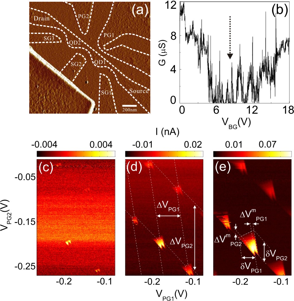
Double quantum dots are a model system for investigating the dynamics of electrons in a wide range of semiconductors Hanson et al. (2007); van der Wiel et al. (2002); Pfund et al. (2006); Schroer et al. (2011); Chorley et al. (2011); Pecker et al. (2013); Zwanenburg et al. (2013). Charge stability diagrams - obtained by measuring the conductance as a function of the carrier density on each quantum dot - reveal a wealth of information about charging energy, interdot coupling and cross gate coupling strength, making them an ideal way to probe charge rearrangments in quantum dots at high magnetic fields. An atomic force microscopy image of the double quantum dot measured in this work is shown in Fig. 1(a). Our device consists of two lithographically etched (O2 plasma) graphene islands each with a size of 200250 nm2 labeled QD1 and QD2 in Fig. 1(a). They are mutually connected to each other by a 90 nm wide constriction and separately connected to the source/drain leads via two 80 nm wide constrictions, which act as tunnel barriers. Two plunger gates PG1(2) are used to tune the energy levels in QD1(2) while three side gates (SG1, SG2 and SG3) are used to tune the tunnel barriers. The doped-silicon back gate (BG) is used to adjust the overall Fermi level.
The measurements were performed in a dilution refrigerator with an electron temperature around 100 mK. In Fig. 1(b), we show the measured differential conductance through DQD as a function of BG voltage (=20 V) highlighting a region of suppressed current (the so-called transport gap Stampfer et al. (2009)) separating the hole from the electron transport regime. At a back gate voltage within the transport gap (=8.61 V, see arrow in Fig. 1(b)) we measure the DC current through DQD as a function of and for a series of applied DC biases as shown in Fig. 1(c) for =400 V, (d) for =1 mV and (e) for =2 mV respectively.
As expected, the current in the stability diagram evolves from triple points into bias-dependent triangles when the bias is increased. The horizontal and vertical measure of the honeycomb cell and (Fig. 1(d)) give the capacitances between the gate PG1 and QD1 =2.77 aF, and between the gate PG2 and QD2 =1 aF. Also the charging energies ==2.57 meV and ==4.77 meV are obtained using the voltage-energy conversion factor =e/ extracted from the bias triangle as shown in Fig. 1(e). The difference in charging energies reflects the fact that the sizes of the dots are not equal and can be justified if the tunnel barriers defined by local disorder potential modify the size of GQDs Liu et al. (2010); Volk et al. (2011). Within this picture, electrons from the source reservoir enter through a large localized state in QD1 ( is small) to a small localized state in QD2 ( is large), and then exit through the drain reservoir. Finally, the interdot coupling energy can be determined from the splitting of the triangles as shown in Fig. 1(e): ==0.29 meV.
III III. Charge stability diagram in perpendicular magnetic field
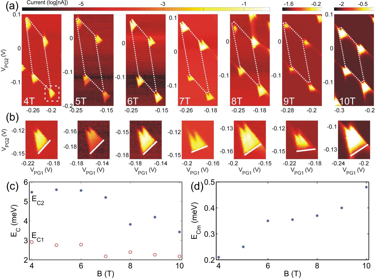
The charge distribution in the QDs can be investigated by looking at how the charge stability diagram evolves under the influence of magnetic field. Fig. 2(a) shows the evolution of a region of the stability diagram, measured at T=100 mK, =8.61 V and =-1 mV, for perpendicular magnetic fields ranging from 4 to 10 T. We have studied the stability diagram in a wide energy range and here only focus on four typical triple points for simplicity. The first observation is the field-dependent change in the dimensions of the honeycomb, which is highlighted by the dotted hexagonal outlines in Fig. 2(a) and is most pronounced from =7 T to =10 T, indicating the variation in the capacitances and . In addition, the close-ups of the triangle in the bottom of each honeycomb, as shown Fig. 2(b), display a change in and , implying that the conversion factors and interdot coupling energy also change with B-field. It is worth noting that the size of triangle varies in the same honeycomb (i.e., B=7 T and B=8 T), indicating the precise size of the localized state can change over a small range of gate voltage. The extracted charging energy of each dot ( and ) and the interdot coupling energy () are shown in Fig. 2(c) and (d) respectively. The QDs charging energies remain roughly unvaried (3 meV, 5.5 meV) from B=4 T to B=6 T then show a decreasing tendency from B=7 T to higher fields. From B=4 to B=10 T, the percentage change in (37.3%) is larger than that in (25%). By contrast, the interdot coupling energy shows a monotonic increase with field from 4 T to 10 T. Our results suggest that both dots increase their size at high B-fields, which reflects on the decreasing charging energies.
IV IV. MODEL AND SIMULATION
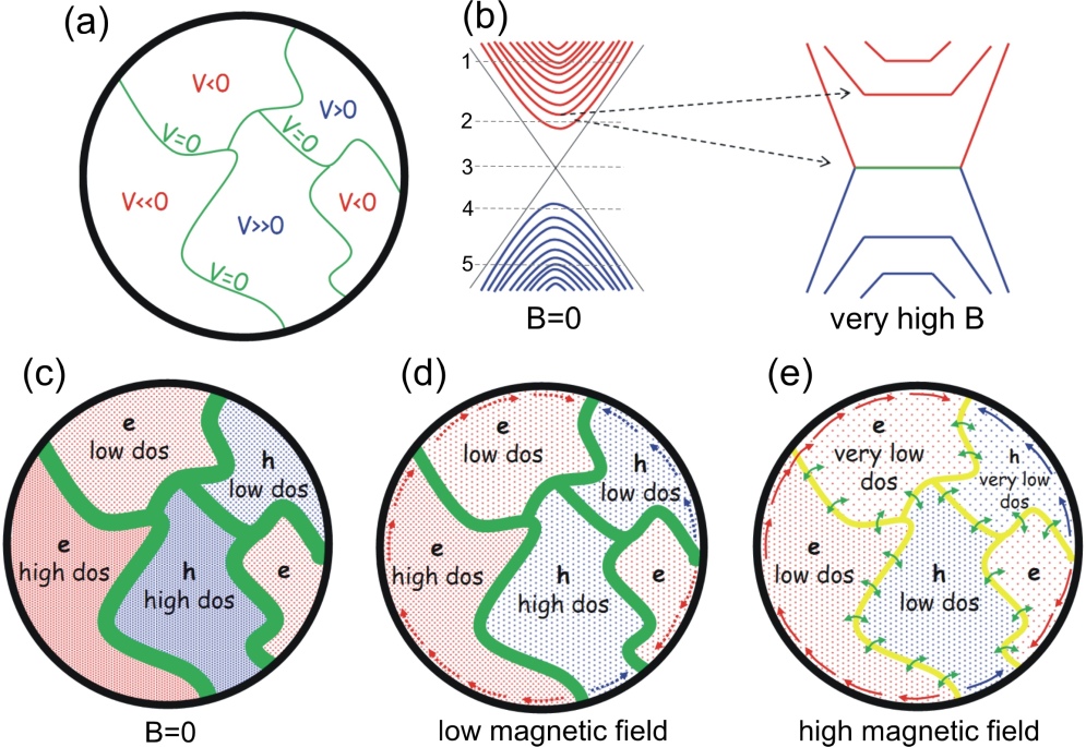
It is well-known that the presence of charged impurities in the SiO2 substrate Zhang et al. (2009); Martin et al. (2008) or surface ripples Deshpande et al. (2009) can induce electron-hole puddles with a size of tens of nanometres in exfoliated graphene flakes. This aspect considerably affects the electronic and transport properties of graphene around the Dirac point and, as we will show, it plays a key role in our case. To take this into account, we consider a varying background potential V in a model QD, as shown in Fig. 3(a), where V fluctuates from positive (red) to negative (blue) passing from V=0 (green). If V varies slowly, in each region of a large dot the energy bands will approximately correspond to the shifted energy bands of 2D graphene, as represented in Fig. 3(b) for zero (left panel) and high (right panel) magnetic field. At B=0 T, a gap is introduced to include the quantum confinement effects due to the dot. This gap progressively reduces at high B-field along with the formation of Landau levels. Depending on the back-gate and background potentials, the Fermi energy (here set to 0) and Dirac point can have locally different relative positions, as indicated by dashed lines in the left panel of Fig. 3(b). The sign and strength of V determine the nature (electron or hole) of the puddles and their density of state (DOS). We first consider the case B=0. For the V0 (V0) regions, the Fermi energy corresponds to level 1 (5) in Fig. 3(b). As the level is far above (below) the charge neutrality point, it gives rise to the electron (hole) puddles with high DOS as shown in Fig. 3(c). In the region where V0 (V0), the Fermi energy corresponds to level 2 (4) and results in electron (hole) puddles with low DOS. In the region around V=0 corresponding to the energy gap, the DOS is very low or 0. These regions (the green region in Fig. 3(c)) separate the puddles and can make the transport diffusive Li et al. (2011).
In the presence of high magnetic fields, due to the formation of LLs, part of the levels around the gap tends to the 0-th Landau level, thus reducing the gap. The other part rises, thus approaching the higher LLs as shown in the right panel of Fig. 3(b), where also the dispersive magnetic edge states are represented. In the low field regime, the LLs are far from being fully established and the DOS in the dot is low. However, the edge channels start developing with opposite chirality for electron and hole puddles as indicated by arrows in Fig. 3(d). At high magnetic field, the LL0 is well developed with the consequent closing of the band gap. Therefore, in the V=0 region the DOS is expected to increase and result in development of non-chiral channels connecting the puddles, as shown in the yellow region in Fig. 3(e). At the same time, the other LLs start developing together with the chiral magnetic edge channels. In this regime, the DOS decreases in the bulk of the puddles while it increases at their edges. Electron transport through the dot is not confined in a particular puddle but can be delocalized in the dot through flowing in both the chiral edge channels (red or blue arrows) and non-chiral channels (yellow region).
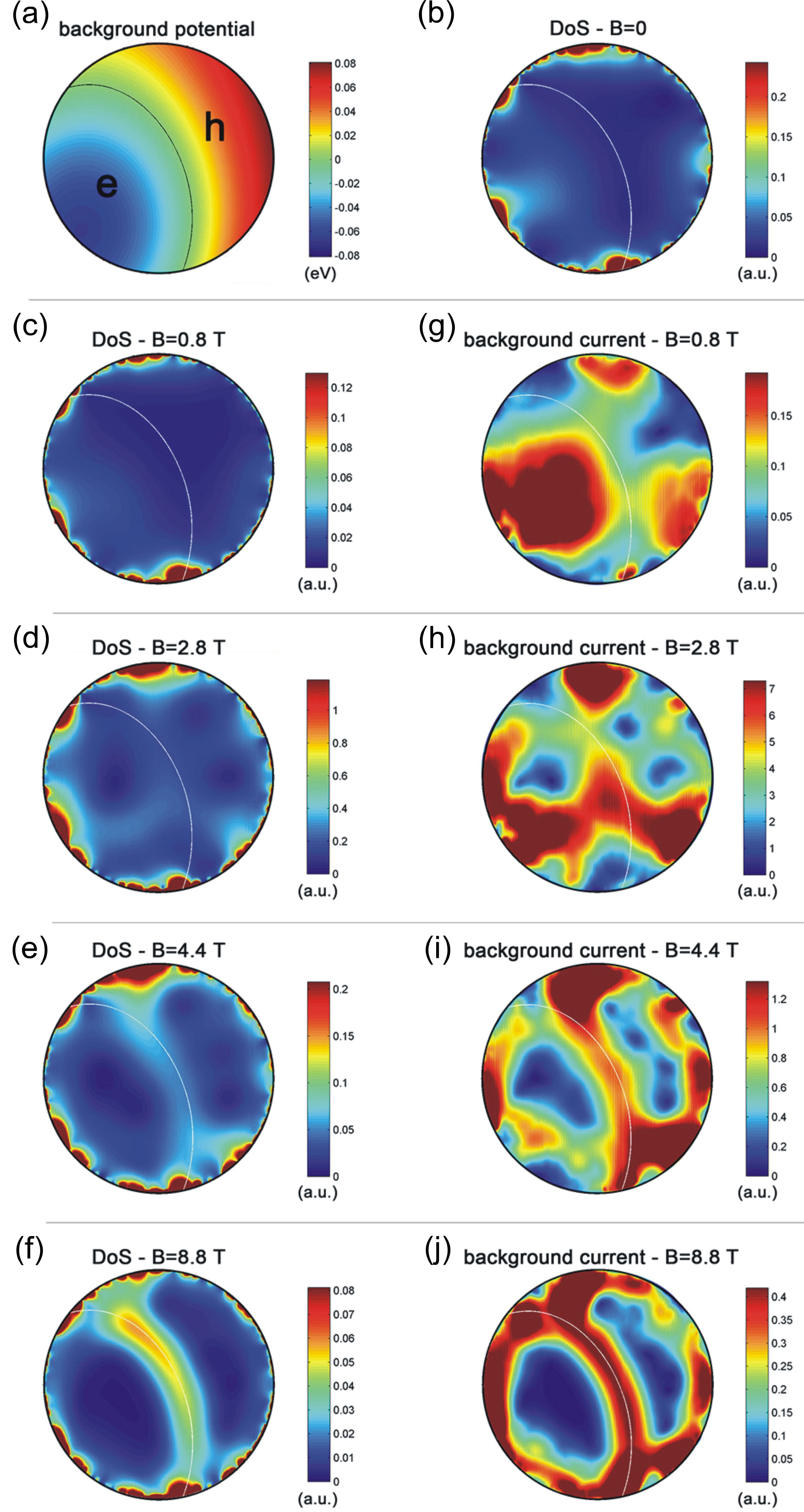
In order to validate this picture, we performed numerical simulations of a QD with radius R=47.5 nm and a background potential consisting of two regions with V0 (81 meV) and V0 (-66 meV), which determine the presence of a hole puddle and an electron puddle, as shown in Fig. 4(a). The dot is described by a first-neighbour tight-binding Hamiltonian with a single orbital per atom and coupling parameter -2.7 eV. For the more details on the Green’s function formalism adopted for the simulations, refer to Ref. Cresti et al. (2006). The calculated DOS of the dot is shown in Fig. 4(b)-(f) in arbitrary units. As expected, at low B (0 and 0.8 T) the DOS is low where V=0 and higher for larger . As B increases (2.8 T), the DOS decreases a little in the centre of the electron/hole puddles, and it increases along the edge due to the progressive developing of magnetic edge states (Fig. 4(d)). Note the presence of very high DOS region at the border of the dot. They correspond to zigzag edge sections, where very localized states appear Nakada et al. (1996). At higher B-field, we observe the presence of high DOS in the V=0 region, which corresponds to the LL0, and the rise of edge states around the dot. The higher the field is, the larger the DOS is in the V=0 and edge regions, as can be seen for B4.4 T in Fig. 4(e) and (f).
The simulated background spectral current distribution (which corresponds to the spatial distribution of the conductive channels) Cresti et al. (2006) in the dot is shown in Fig. 4(g)-(j). At low magnetic field (B0.8 T) the current is mainly concentrated in the high regions and the V=0 region seems to act as a barrier between the two puddles. At slightly higher field (B=2.8 T) the current starts tending to the V=0 region due to the progressive closing of the energy gap. At high fields (B4.4 T), we observe the current flowing along the chiral magnetic edge states of the dot and along the non-chiral V=0 region, where the gap is now closed. In this regime, the current is delocalized in the dot and a charge rearrangemet can be seen compared to the case at low B-fields. Note that the more fractured the disorder potential is (meaning more existing electron/hole puddles) the more pronounced the charge delocalization effect will be at high fields.
V V. Discussion
As the back gate voltage (=8.61 V) where all the measurements were carried out is near the charge neutrality point, it is expected the background potential fluctuations will play a role and give rise to electron-hole puddles formed in the QDs Martin et al. (2008); Connolly et al. (2010). In this situation, our model can be readily adapted to explain the data. Due to the closing of the energy gap at high enough magnetic fields, at the V=0 region the DOS is high and develops non-chiral channels which connect the puddles, as sketched in Fig. 3(e). Hence, the current can flow through the puddles via crossing the high DOS non-chiral channels at the interface, thus making electrons no longer confined in a particular puddle but delocalized in a larger puddle, resulting in a smaller charging energy. Here we point out that the field has to be high enough for the LLs and edge states to be fully developed to close the energy gap. The threshold B-field for this to happen in a GSQD with a relatively smaller size (50 nm diameter) is around 10 T Guttinger et al. (2009). As a result, the change in charging energies in our case is most pronounced from B=6 T to B=10 T for QD1 and from B=7 T to B=10 T for QD2, as shown in Fig. 2(c). The threshold B-field for QD2 is higher owing to its larger charging energy (smaller puddle), in which the magnetic length = has to be comparable or even smaller than the puddle size. The magnetic length for B=7 T is around 9 nm, implying the size of puddle in the dot is around (or more than) twice the critical magnetic length, in good agreement with the puddle size (20 nm) measured in graphene Zhang et al. (2009). In addition, we observed the change in from B=4 T to B= 10 T is larger than that in . This is expected, since is smaller than , indicating electrons tunnel through a larger localized state in QD1 and a smaller localized state in QD2. In other words, the disorder potential in QD2 is more fractured than that in QD1. Therefore, at high B-field the charge delocalization effect is more pronounced in QD2 than that in QD1, giving rise to the larger B-dependent charging energy in QD2. Here we note that the GQD has to be large for the substrate disorder to play an important role, which may be the reason that the decreasing charging energy with B-field is not observed in other relatively smaller GQD with large edge-to-bulk ratio Guttinger (2008); Guttinger et al. (2009) or GQD on hBN Epping et al. (2013) where substrate disorder is less important. The increasing interdot coupling energy may be also understood as the charges rearranging from the center of the puddles to the edge of the dot (see Fig. 4 (g)-(j)). This scenario depends on the progressively formed edge state with increasing B-field, and can be observed in the whole range of B-field (Fig. 2(d)).
A more recent study of GNR on hBN substrate has indicated that the localized states may also extend into the leads of the device, giving rise to smaller charging energies than expected from the geometry of GNR alone Bischoff et al. (2014). However, two conditions are crucial for this effect to be seen. One is the substrate disorder has to be much weaker than the edge disorder, and the other is the edge-to-bulk ratio of device has to be large enough for the edge to play an important role. Transport in GQDs on hBN is dominated by the edge roughness for QDs with diameter less than 100 nm Engels et al. (2013). Each condition is met by their relatively small GNR (30 nm 30 nm) on hBN, thus the edge disorder is strong enough to localize electron wavefunction along the edge to the leads. On the contrary, our large dot (and the tunnel barrier GNR) with smaller edge-to-bulk ratio should diminish the influence of the rough edges on overall transport, meaning localization along the edge still happens but transport is dominated by bulk contributions. Therefore, we argue that the charge redistribution (based on substrate disorder) in our QDs is the main factor that leads to a variation of dots area and contribute to the decreasing charging energies in magnetic fields.
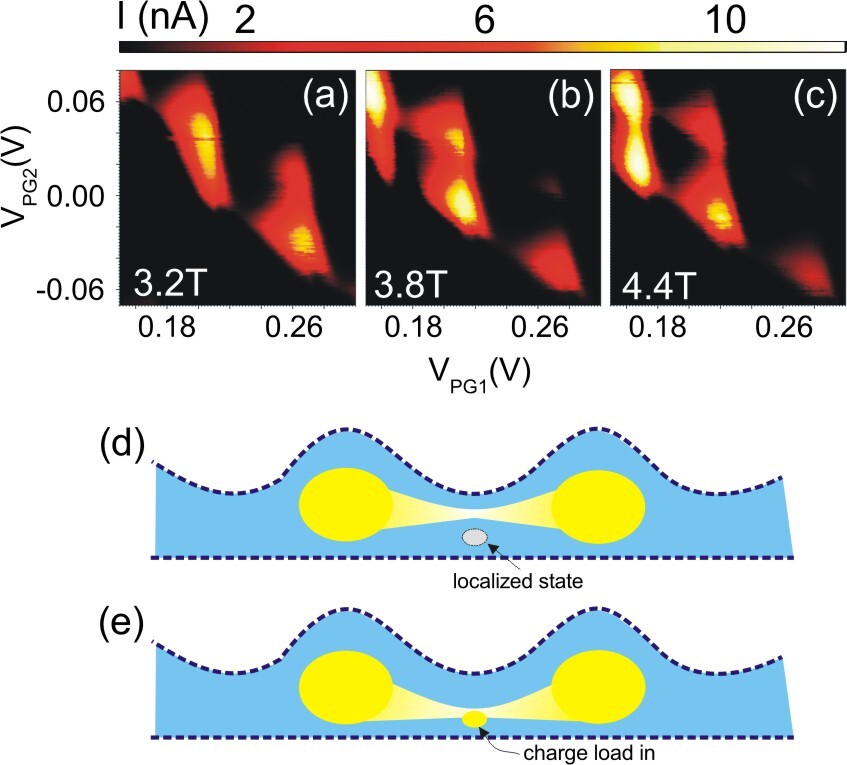
The effect of disorder can be also seen in Fig. 5, where a stability diagram measured in different cool-down of device at B-fields (a) 3.2 T, (b) 3.8 T and (c) 4.4 T is presented. The triangle shape first distorts at B=3.2 T and then splits into two separated ones (Fig. 5 (b)), then moves further apart and form an additional row of triangles (Fig. 5 (c)). We attribute this newly appeared triangles to the formation of a localized state in a magnetic field, which is capacitively coupled to the original dots Guttinger et al. (2011); Wei et al. (2013). A schematic illustration is shown in Fig. 5 (d) and (e) to address such a scenario. When a localized state is formed in magnetic field, while the gate voltage is sweeped it can add or subtract charges discretely to the parasitic dot, thus altering the entire environment abruptly and unexpectedly. The fact that the splitting occurs on both gate spaces suggests the localized state can affect two dots in a similar way, implying its location is in the central GNR (Fig. 5 (d)). The new dot acts as a gate which will shift the triple-points in charge stability diagram, consequently, leading to an additional row of triangles adding adjacent to the original ones.
VI VI. Summary
In summary, we have fabricated and studied the magneto-transport properties of a large GDQD device. In different cool downs, we observed a honeycomb pattern which is typical of charge stability diagrams for a DQD system. We studied the evolution of the charge stability diagram under the influence of B-field up to 10 T. The charging energy and the interdot coupling energy show different dependence with B-field, suggesting the size of both dots become larger in high field. Our interpretation is supported by numerical simulations in which we show the confined charges in the puddles of GQDs can be redistributed from the bulk to the edge through the formation of LLs and edge states. At high enough B-field, due to the closing of energy gap, electrons are delocalized via crossing the non-chiral channels connecting different puddles, resulting in a smaller charging energy.
This work was financially supported by the EPSRC. Additional data related to this publication is available at the xxxxxxx data repository.
References
- Geim and Novoselov (2007) A. K. Geim and K. S. Novoselov, Nat Mater 6, 183 (2007), ISSN 1476-1122, URL http://dx.doi.org/10.1038/nmat1849.
- Huertas-Hernando et al. (2009) D. Huertas-Hernando, F. Guinea, and A. Brataas, Phys. Rev. Lett. 103, 146801 (2009), URL http://link.aps.org/doi/10.1103/PhysRevLett.103.146801.
- Guttinger (2008) J. Guttinger, Applied Physics Letters 93, 212102 (2008), URL http://dx.doi.org/doi/10.1063/1.3036419.
- Volk et al. (2013) C. Volk, C. Neumann, S. Kazarski, S. Fringes, S. Engels, F. Haupt, A. Muller, T.ller, and C. Stampfer, Nat Commun 4, 1753 (2013), URL http://dx.doi.org/10.1038/ncomms2738.
- Guttinger et al. (2009) J. Guttinger, C. Stampfer, F. Libisch, T. Frey, J. Burgdorfer, T. Ihn, and K. Ensslin, Phys. Rev. Lett. 103, 046810 (2009), URL http://link.aps.org/doi/10.1103/PhysRevLett.103.046810.
- Molitor et al. (2010) F. Molitor, H. Knowles, S. Droscher, U. Gasser, T. Choi, P. Roulleau, J. Guttinger, A. Jacobsen, C. Stampfer, K. Ensslin, et al., EPL (Europhysics Letters) 89, 67005 (2010), URL http://stacks.iop.org/0295-5075/89/i=6/a=67005.
- Liu et al. (2010) X. L. Liu, D. Hug, and L. M. K. Vandersypen, Nano Letters 10, 1623 (2010), ISSN 1530-6984, URL http://dx.doi.org/10.1021/nl9040912.
- Connolly et al. (2013) M. R. Connolly, K. L. Chiu, S. P. Giblin, M. Kataoka, J. D. Fletcher, C. Chua, J. P. Griffiths, G. A. C. Jones, V. I. Fal’ko, and C. G. S. T. J. B. M. Janssen, Nat Nano 8, 417 (2013), ISSN 1748-3387, URL http://dx.doi.org/10.1038/nnano.2013.73.
- Engels et al. (2013) S. Engels, A. Epping, C. Volk, S. Korte, B. Voigtlander, K. Watanabe, T. Taniguchi, S. Trellenkamp, and C. Stampfer, Applied Physics Letters 103, 073113 (2013), URL http://scitation.aip.org/content/aip/journal/apl/103/7/10.1063/1.4818627.
- Epping et al. (2013) A. Epping, S. Engels, C. Volk, K. Watanabe, T. Taniguchi, S. Trellenkamp, and C. Stampfer, Phys. Status Solidi B 250, 2692 (2013), ISSN 1521-3951, URL http://dx.doi.org/10.1002/pssb.201300295.
- Chiu et al. (2012) K. L. Chiu, M. R. Connolly, A. Cresti, C. Chua, S. J. Chorley, F. Sfigakis, S. Milana, A. C. Ferrari, J. P. Griffiths, G. A. C. Jones, et al., Phys. Rev. B 85, 205452 (2012), URL http://link.aps.org/doi/10.1103/PhysRevB.85.205452.
- Guttinger et al. (2010) J. Guttinger, T. Frey, C. Stampfer, T. Ihn, and K. Ensslin, Phys. Rev. Lett. 105, 116801 (2010), URL http://link.aps.org/doi/10.1103/PhysRevLett.105.116801.
- Volk et al. (2011) C. Volk, S. Fringes, B. Terres, J. Dauber, S. Engels, S. Trellenkamp, and C. Stampfer, Nano Letters 11, 3581 (2011), ISSN 1530-6984, URL http://pubs.acs.org/doi/abs/10.1021/nl201295s.
- Amet et al. (2012) F. Amet, J. R. Williams, A. G. F. Garcia, M. Yankowitz, K. Watanabe, T. Taniguchi, and D. Goldhaber-Gordon, Phys. Rev. B 85, 073405 (2012), URL http://link.aps.org/doi/10.1103/PhysRevB.85.073405.
- Hanson et al. (2007) R. Hanson, L. P. Kouwenhoven, J. R. Petta, S. Tarucha, and L. M. K. Vandersypen, Rev. Mod. Phys. 79, 1217 (2007), URL http://link.aps.org/doi/10.1103/RevModPhys.79.1217.
- van der Wiel et al. (2002) W. G. van der Wiel, S. De Franceschi, J. M. Elzerman, T. Fujisawa, S. Tarucha, and L. P. Kouwenhoven, Rev. Mod. Phys. 75, 1 (2002), URL http://link.aps.org/doi/10.1103/RevModPhys.75.1.
- Pfund et al. (2006) A. Pfund, I. Shorubalko, R. Leturcq, and K. Ensslin, Applied Physics Letters 89, 252106 (2006), URL http://scitation.aip.org/content/aip/journal/apl/89/25/10.1063/1.2409625.
- Schroer et al. (2011) M. D. Schroer, K. D. Petersson, M. Jung, and J. R. Petta, Phys. Rev. Lett. 107, 176811 (2011), URL http://link.aps.org/doi/10.1103/PhysRevLett.107.176811.
- Chorley et al. (2011) S. J. Chorley, G. Giavaras, J. Wabnig, G. A. C. Jones, C. G. Smith, G. A. D. Briggs, and M. R. Buitelaar, Phys. Rev. Lett. 106, 206801 (2011), URL http://link.aps.org/doi/10.1103/PhysRevLett.106.206801.
- Pecker et al. (2013) S. Pecker, F. Kuemmeth, A. Secchi, M. Rontani, D. C. Ralph, P. L. McEuen, and S. Ilani, Nat Phys 9, 576 (2013), ISSN 1745-2473, URL http://dx.doi.org/10.1038/nphys2692.
- Zwanenburg et al. (2013) F. A. Zwanenburg, A. S. Dzurak, A. Morello, M. Y. Simmons, L. C. L. Hollenberg, G. Klimeck, S. Rogge, S. N. Coppersmith, and M. A. Eriksson, Rev. Mod. Phys. 85, 961 (2013), URL http://link.aps.org/doi/10.1103/RevModPhys.85.961.
- Stampfer et al. (2009) C. Stampfer, J. Guttinger, S. Hellmuller, F. Molitor, K. Ensslin, and T. Ihn, Phys. Rev. Lett. 102, 056403 (2009), URL http://link.aps.org/doi/10.1103/PhysRevLett.102.056403.
- Zhang et al. (2009) Y. Zhang, V. W. Brar, C. Girit, A. Zettl, and M. F. Crommie, Nat Phys 5, 722 (2009), ISSN 1745-2473, URL http://dx.doi.org/10.1038/nphys1365.
- Martin et al. (2008) J. Martin, N. Akerman, G. Ulbricht, T. Lohmann, J. H. Smet, K. von Klitzing, and A. Yacoby, Nat Phys 4, 144 (2008), ISSN 1745-2473, URL http://dx.doi.org/10.1038/nphys781.
- Deshpande et al. (2009) A. Deshpande, W. Bao, F. Miao, C. N. Lau, and B. J. LeRoy, Phys. Rev. B 79, 205411 (2009), URL http://link.aps.org/doi/10.1103/PhysRevB.79.205411.
- Li et al. (2011) Q. Li, E. H. Hwang, and S. Das Sarma, Phys. Rev. B 84, 115442 (2011), URL http://link.aps.org/doi/10.1103/PhysRevB.84.115442.
- Cresti et al. (2006) A. Cresti, G. Grosso, and G. P. Parravicini, Eur. Phys. J. B 53, 537 (2006), URL http://dx.doi.org/10.1140/epjb/e2006-00408-2.
- Nakada et al. (1996) K. Nakada, M. Fujita, G. Dresselhaus, and M. S. Dresselhaus, Phys. Rev. B 54, 17954 (1996), URL http://link.aps.org/doi/10.1103/PhysRevB.54.17954.
- Connolly et al. (2010) M. R. Connolly, K. L. Chiou, C. G. Smith, D. Anderson, G. A. C. Jones, A. Lombardo, A. Fasoli, and A. C. Ferrari, Appl. Phys. Lett. 96, 113501 (2010), URL http://link.aip.org/link/?APL/96/113501/1.
- Bischoff et al. (2014) D. Bischoff, F. Libisch, J. Burgdörfer, T. Ihn, and K. Ensslin, Phys. Rev. B 90, 115405 (2014), URL http://link.aps.org/doi/10.1103/PhysRevB.90.115405.
- Guttinger et al. (2011) J. Guttinger, C. Stampfer, T. Frey, T. Ihn, and K. Ensslin, Nanoscale Research Letters 6, 253 (2011), ISSN 1556-276X, URL http://www.nanoscalereslett.com/content/6/1/253.
- Wei et al. (2013) D. Wei, H.-O. Li, G. Cao, G. Luo, Z.-X. Zheng, T. Tu, M. Xiao, G.-C. Guo, H.-W. Jiang, and G.-P. Guo, Sci. Rep. 3, (2013), URL http://dx.doi.org/10.1038/srep03175.