Phonon-thermoelectric transistors and rectifiers
Abstract
We describe nonlinear phonon-thermoelectric devices where charge current and electronic and phononic heat currents are coupled, driven by voltage and temperature biases, when phonon-assisted inelastic processes dominate the transport. Our thermoelectric transistors and rectifiers can be realized in a gate-tunable double quantum-dot system embedded in a nanowire which is realizable within current technology. The inelastic electron-phonon scattering processes are found to induce pronounced charge, heat, and cross rectification effects, as well as a thermal transistor effect that, remarkably, can appear in the present model even in the linear-response regime without relying on the onset of negative differential thermal conductance.
pacs:
73.23.-b,73.50.Fq,73.50.Lw,85.30.PqI Introduction
Onsager’s formulation of irreversible thermodynamics and his famous reciprocal relations (1931)Onsager (1931), based on the time reversibility of microscopic dynamics, tie different currents to driving forces (affinities) and provide strict bounds on the efficiency of energy transducers Jiang (2014a). Among such transport phenomena the thermoelectric effect which describes the coupling of electronic charge and heat currents nowadays attracts significant attention experimentally, computationally, and fundamentally, as new-unique thermoelectric materials and devices are pursued with a promise for an improved efficiency, see e.g. Refs. Dresselhaus et al., 2007; Vineis et al., 2010; Malen et al., 2010; Hochbaum and Yang, 2010; Dubi and Di Ventra, 2011; Shakouri, 2011; Sothmann et al., 2015. The thermoelectric effect has been traditionally characterized by linear response quantities, Seebeck and Peltier coefficients. Nonlinear thermoelectric phenomena constitute a new area of research, anticipated to enhance thermoelectric response Vashaee and Shakouri (2004); Zebarjadi et al. (2007); Meair and Jacquod (2013); Leijnse et al. (2010). An elastic scattering theory of nonlinear thermoelectric transport has been recently developed by considering self-consistent screening potentials Meair and Jacquod (2013); Sánchez and López (2013); López and Sánchez (2013); Argüello-Luengo et al. (2015); Hwang et al. (2015); Svensson et al. (2013); Whitney (2013a, b). Other studies had considered nonlinear thermoelectric transport with explicit electron-electron Kuo and Chang (2010); Azema et al. (2014), electron-phonon Leijnse et al. (2010) and electron-photon Henriet et al. (2015) interactions. However, an investigation of nonlinear inelastic “phonon-thermoelectric” systems, where charge current and electronic and phononic heat currents are coupled, and non-linear thermoelectric device operations (such as rectifiers and transistors) is still missing.
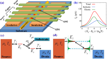
By “phonon-thermoelectric” systems, we refer to a setup first considered in Ref. Entin-Wohlman et al., 2010 (see also, Refs. Jiang et al., 2012, 2013; Jiang, 2014b), where electrical and thermal heat currents from source to drain were induced and manipulated by a third, independent, phonon reservoir. This terminal is characterized by its temperature, which is possibly distinct from the temperatures of the source and drain. The physical mechanisms involving the phonon baths are inelastic-phonon assisted electron hopping from the source to the drain. In the setup shown in Fig. 1(a), the substrate corresponds to the third terminal, and it determines the temperature of phonons. In the linear response regime, a hot phonon bath can pump electrical current, to drive electrons against the electrochemical potential gradient. This effect was termed as the “three-terminal thermoelectric effect”, and it is similar to the photo-electric effect in photovoltaic systems where high-temperature photons pump electric currents. In fact, this analogy has been utilized for proposing useful thermoelectric devicesJiang et al. (2013). Here, we extend this mechanism to the nonlinear response regime, to realize nontrivial thermoelectric functions and devices.
Nonlinear electrical elements, diodes, amplifiers, and transistors, are key components in electronics, at the heart of modern technology. More recently, significant efforts have been devoted to the exploration of analogous phononic elements at the nanoscale Li et al. (2012). These endeavors, nonlinear nanoelectronic and nanophononic, were often separately pursued. However, it is to be noted that in many cases the interaction of electrons with the atomic degrees of freedom (vibrations, phonons) cannot be ignored. While electron-phonon dissipation effects often impede device operation, here we exploit them to achieve compound nonlinear functionalities. We demonstrate these functionalities in a three-terminal geometry (the simplest situation). The effects described here can be generalized to other situations in which electronic currents and phononic currents are spatially separated.
In this work, we provide a unified description of coupled and nonlinear electrical and phononic transport in the three-terminal geometry when inelastic electron-phonon scatterings play a key role. The nonlinear, inelastic electron transport in our geometry (see Fig. 1) provides charge and thermal rectification, cross-rectification effects (e.g., thermal rectification induced by voltage), as well as the realization of the thermal transistor effect and a phonon-thermoelectric cross effect (e.g., controlling source-drain - characteristics by modulating the temperature of a third terminal). Remarkably, we find that in the linear response regime inelasticity can lead to a thermal transistor effect. This is in contrast to common wisdom Li et al. (2006, 2012) that thermal transistor effect must comply with negative differential thermal conductance. The essential ingredient here is that inelastic electron-phonon scattering processes simultaneously involve three different reservoirs. This mechanism also works for inelastic electron transport assisted by coulomb drag effects Sánchez et al. (2010); Sothmann et al. (2012), magnons Sothmann and Büttiker (2012), photons Rutten et al. (2009); Juergens et al. (2013), and plasmons Torre et al. (2015), thus our results are of interest beyond the specific model considered in this work.
II Model system
We consider a double quantum-dot (DQD) embedded in a nanowire in contact with two metals and a phonon substrate (“”), see Fig. 1. The quantum dots (QDs) are defined by voltage gates (labeled by and in Fig. 1a) with tunable electronic energy levels and . is a hopping element between the QDs and are the hybridization energies of the dots to the source and drain electrodes, labeled by and , respectively. Charge current, electronic heat current, and phononic heat current are induced by applying a voltage bias between the terminals and and a temperature difference between the three terminals. This setup (and related models) have been explored in e.g., Refs. Koch et al., 2004; Segal, 2005; Ren et al., 2012; Kulkarni et al., 2014; Thierschmann et al., 2015; Koch et al., 2014; Arrachea et al., 2014; Zhou et al., 2015; Simine et al., 2015; Entin-Wohlman et al., 2010; Jiang et al., 2012, 2013. However, previous studies had focused on the linear response regime, while here we uncover coupled nonlinear phenomena. The system is described by the Hamiltonian,
| (1) |
with
| (2a) | |||
| (2b) | |||
| (2c) | |||
| (2d) | |||
| (2e) | |||
Here () creates an electron in the -th QD with an energy . The () QD is located next to the left (right) lead. The tunneling elements from the QD to the right lead and that from the QD to the left lead are assumed negligible. Electron-phonon interactions (matrix element ) allow inelastic electron transport through the system; creates a phonon with a wavevector and frequency . We adopt the conventions that and throughout the paper. To maintain a finite temperature difference between the electrodes and the substrate, we suggest to thermally isolate them with a layer of thermal and electrical insulation [see Fig. 1(a)]. The phonons involved in the inelastic transport through the DQD system may be confined phonons in the quantum wire, or bulk phonons in the substrate. We assume the thermal contact between the quantum wire and the substrate to be good so that these two types of phonons acquire the same temperature . The phonon temperature can be controlled by the substrate, while the temperature of the electrodes ( and ) can be individually controlled by heating them with, e.g., AC electric fields Giazotto et al. (2006); Dubi and Di Ventra (2011). Although Coulomb interaction is certainly important in electron transport effects through QDs, to simplify the problem and to uncover the essential physics, we assume that the intra-dot Coulomb interaction energy is much larger than other relevant energy scales in our problem, as well as that the inter-dot Coulomb interaction is small and negligible. Under these assumptions, we can ignore the Coulomb interaction altogether. This assumption limits our discussions to the regime where there is no more than one electron in each QD. Nevertheless, the essential element for the phenomena described in this work is energy exchange between electrons and phonons, rather than electron-electron energy exchange process.
III Currents in and beyond linear-response
Non-equilibrium steady state quantities of interest are the electric current , the electronic heat current traversing from the left lead to the right lead , and the phonon heat current , with () denoting the heat current flowing into the th reservoir. Both elastic and inelastic processes contribute to transport in the system [see panels (b), (c) and (d) in Fig.1].
The inelastic (“inel”) contribution to the currents is calculated from the Fermi Golden-Rule treatment of Ref. Jiang et al., 2012, setting for convenience ,
| (3) |
Here is the charge of an electron, , and . In the above equation, with and . Here with the Bose-Einstein distribution for phonons . For the commonly used zinc blend semiconductors such as GaAs and InP, the electron-phonon interaction energy determines the transition rateFedichkin and Fedorov (2004); Wu et al. (2005); Weber et al. (2010); Kulkarni et al. (2014) . Here stands for the electron-phonon scattering strength, provides the power-law dependence on phonon energy with a characteristic energy . Appendix A provides details on the derivation of this expression from the microscopic theory of electron-phonon interactions in GaAs QDs. It is found that in this system the piezoelectric mechanism dominates the electron-phonon interaction. In this situation, we adopt the parameters eV and Weber et al. (2010); Kulkarni et al. (2014). The Fermi Golden Rule method is valid when Jiang et al. (2012). These conditions can be maintained by tuning the coupling between the QDs and the leads. In this regime, the steady state distributions on the two QDs can be approximated by those of the nearby leads Jiang et al. (2012), i.e., and , where and are the Fermi distribution functions for the left and right electronic reservoirs, respectively. If the Fermi Golden Rule assumptions (specifically, the second inequality) are not satisfied, the inelastic current can be calculated more generally via a rate equation technique [see Appendix B]. The Fermi Golden Rule method is exploited below for the analytic study of transport coefficients. Numerical results in this work are calculated directly from the rate equation method (unless specified otherwise).
The contribution of elastic (“el”) processes to the currents is given by Landauer’s formula
| (4a) | ||||
| (4b) | ||||
Note that elastic processes do not contribute to the heat current from the phonon terminal . The energy-dependent transmission function is obtained from the Caroli formula, , where , , and , where we assume constant (energy-independent) tunneling rates and . This results in with . In Fig. 1(b) we plot the elastic contribution to the charge current (green) as a function of the DQD level detuning for an otherwise symmetric junction . As expected, the current is an even function with respect to detuning. In contrast, the inelastic contribution (blue) is asymmetric with respect to detuning. This distinction serves as a signature of inelastic transport in DQD systems in experiments Kulkarni et al. (2014). Contributions from elastic transport processes are included in our simulations.
The entropy production rate for the whole system is given by
| (5) |
where the affinities for , , and [identified in Eq. (5) by separately], are , respectively. By setting the reference temperature at , we obtain , , and where , , and Jiang et al. (2012). Note that the reference temperature is defined according to [differing from the average temperature in nonlinear-response regime]Andrieux and Gaspard (2004).
Expanding Eqs. (3) and (4) to capture nonlinear effects, we find, to the lowest nontrivial order
| (6) |
where with denoting the linear-response coefficients. The Onsager reciprocal relations, , hold for both elastic and inelastic transport processes. The second-order terms only come up from the inelastic transport processes. Elastic coefficients are given by
| (7a) | |||
| (7b) | |||
| (7c) | |||
| (7d) | |||
The superscript denotes the equilibrium distribution. The linear response inelastic coefficients which satisfy the Onsager reciprocal relations are
| (8) |
where is the transition rate from QD to QD at equilibrium, and .
The second-order transport coefficients are given by
| (9) |
where ()
| (10) |
Note that Onsager reciprocal symmetry does not guarantee Andrieux and Gaspard (2004).
For the described functionalities to be prominent, the contribution from the inelastic processes needs to be enhanced while the elastic processes must be suppressed. This is realized by strong electron-phonon interaction, high temperatureJiang et al. (2012), and the mismatch of QDs energy levels. The latter creates a barrier for elastic tunneling and favors inelastic transport. We noticed from Fig. 1(b) that there is an optimal alignment of QDs energy levels for inelastic processes to be dominant. It is also noted that the inelastic contribution is nonzero even at , which is a special property of the piezoelectric electron-phonon interaction: The electron-phonon coupling strength is proportional to , but this linear dependence cancels out the divergence in the phonon number in the limit , overall leaving a finite term which contributes to the current. A careful examination of the limit for realistic systems is beyond the scope of this paper. Our main conclusions do not rely on the behavior of the system in this special regime.
The transport coefficients depend on the average energy (representing deviation from particle-hole symmetry) and the detuning (measuring deviation from mirror symmetry). The symmetry of transport coefficients and currents under (i) particle-hole transformation: (hence and ) and (ii) mirror symmetry (assuming ) (i.e., ) are summarized in Table I. These symmetries rule out certain nonlinear effects in the presence of mirror symmetry and/or particle-hole symmetry. For example, when but only terms of the same symmetry under the particle-hole and mirror transformations remain nonzero.
| Terms | Particle-hole | Mirror | ||
|---|---|---|---|---|
| , , | Odd | Odd | ||
| Even | Odd | |||
| , , , | Odd | Odd | ||
| , , , | Even | Odd | ||
| , , | Even | Even | ||
| , , | Odd | Even | ||
| , | Odd | Odd | ||
| Even | Odd | |||
| , , | Even | Even |
| Terms () | Diode or Transistor effect | |
|---|---|---|
| charge rectification | ||
| , | electronic and phononic heat rectification | |
| , | off-diagonal heat rectification | |
| , | charge rectification by or | |
| , | heat rectification by voltage | |
| , | other nonlinear thermoelectric | |
| phonon-thermoelectric transistor |
IV Rectification (diode) effect
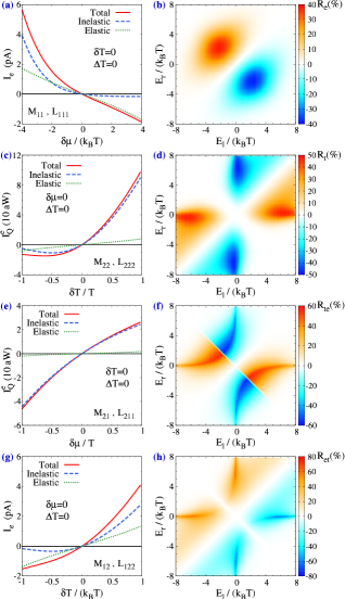
Coupled thermal and electrical transport allows unconventional rectification, for example, charge rectification induced by a temperature difference, besides showing the standard charge and heat rectification effects. The magnitude of the rectification effect is defined by for charge rectification, for (electronic) heat rectification, for charge rectification induced by the temperature difference , and for heat rectification induced by voltage bias. We shall refer to and as “thermoelectric rectifications”. The dependence of these quantities on the DQDs energies is displayed in Fig. 2, demonstrating significant rectification effects.
From these figures, one finds that thermal diode and thermoelectric diode cannot be realized when the system is invariant under (i.e., vanishing ). In Table II we classify second-order transport coefficients as rectifiers and transistors. We note that the rectification and transistor behavior as displayed in Fig.2 [obtained from a direct calculation using Eqs. (3)-(4)], acquire the same symmetry as the corresponding second-order transport coefficients listed in Table 2. Specifically, and (relating to and , respectively) are odd under both and , whereas and (relating to and , respectively) are even under , but odd under . In addition, it is demonstrated in Fig.2 that one can tune and for reaching optimal electrical, thermal, and cross rectifications.
V Transistors
One of our central results is that a thermal transistor effect can develop in the linear-response regime. Specifically, the heat current amplification factor is given by
| (11) |
where is the heat current flowing out of the electrode (since ). Eq. (11) follows directly from (i) , [according to Eq. (3)], and (ii) the elastic contribution to does not depend on the phonon temperature . Hence
| (12) |
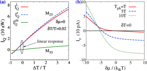
and one obtains Eq. (11). Remarkably, heat current amplification, , is achievable once in both the linear and nonlinear regimes whenever the inelastic contribution is nonzero. This conclusion counters present designs in which a thermal transistor effect can only be realized in the nonlinear response regime based on a negative differential thermal conductance Li et al. (2006). In fact, one can prove that a thermal transistor effect can materialize in the linear response regime only when inelastic processes involve more than two reservoirs due to restrictions imposed by the second law of thermodynamics [see Appendix C]Jiang et al. (2015). The inelastic electron hopping mechanism assumed in our three-terminal setup is one of the simplest examples which can realize such a nontrivial property: electrons enter from the source and leave at the drain with the assistance of phonons from a third terminal (the substrate). Fig.3(a) demonstrates the thermal transistor behavior: changes more significantly than . Specifically, for the adopted temperature difference and for small the system is indeed described by linear response terms. Although the coefficient increases for smaller , the variation of the heat current as controlled by the temperature of the phonon terminal can also decrease once the inelastic transport mechanism weakens [see Fig. 1(b)].
In addition to the thermal transistor effect exemplified in Fig.3(a), we also show in Fig.3(b) that by changing the temperature of the phonon bath we can substantially modify the - characteristics — This effect is analogous to the field effect transistor, but here it is controlled by the phonon temperature instead of the gate voltage at the third terminal. This functionality is also different from the unconventional transistor effect observed in superconductor–normal-metal–superconductor junctions by Saira et al. where gate-voltage at the third terminal controlled thermal transport between source and drain using the Coulomb blockade in the normal-metal regionSaira et al. (2007).
VI Conclusions and discussions
We proposed a realistic and relatively simple setup for the realization of thermal, electrical, and cross rectifiers and transistors by exploiting phonon-assisted hopping transport in DQD systems in a three-terminal geometry. While we used a DQD system embedded in a phonon substrate as our platform, results are applicable to other two-site (two-level) systems maintained out of equilibrium by multiple biases and subjected to inelastic transport processes. Numerical simulations using realistic parameters demonstrate strong charge, heat and thermoelectric rectifications. Furthermore, for the first time, it is observed that a thermal transistor can be realized without negative differential thermal conductance. In addition, a transistor effect where the - characteristics is tuned by the phonon temperature was revealed. These functionalities should enable smart manipulations of heat and charge transport in nano-systems, core elements in future information processing technologies. Although calculations were performed for a specific set of parameters, the uncovered functionalities should be observed whenever inelastic transport processes dominate elastic effects. As discussed in Refs. Jiang et al., 2012, 2013, this can be achieved in the high temperature and strong electron-phonon interaction regime when elastic transport is suppressed e.g. by a barrier, or an energy gap. Our study here essentially aimed at the hybridization of two distinct branches of technology: electronics and phononicsLi et al. (2012). Amalgamation of technologies may provide new platforms and opportunities for high-performance, high-energy-efficiency nanotechnologies. Extensions to consider the interplay of spin, charge, and heat transport in the presence of inelastic effects are of interest for exploring spin-caloritronics Bauer et al. (2012) devices beyond linear response. The physics revealed here, i.e., the essential importance of inelastic transport effects for a linear-response transistor and other nonlinear device functionalities, is also of importance for related research fields.
VII Acknowledgments
JHJ acknowledges support from the faculty start-up funding of Soochow University. MK thanks the hospitality of the Chemical Physics Theory Group at the Department of Chemistry of the University of Toronto and the Initiative for the Theoretical Sciences (ITS) - City University of New York Graduate Center where several interesting discussions took place during this work. He also gratefully acknowledges support from the Professional Staff Congress – City University of New York award No. 68193-0046. DS acknowledges support from an NSERC Discovery Grant and the Canada Research Chair program. YI acknowledges support from the Israeli Science Foundation (ISF) and the US-Israel Binational Science Foundation (BSF).
Appendix A Derivation of the phonon induced transition rate between DQDs.
The electron-phonon coupling matrix for longitudinal phonons in GaAs is given by
| (13) |
where is the volume of the system, kg/m3 is the mass density of GaAs, eV is the deformation potential, and m/s is the velocity of longitudinal phonons. The piezoelectric potential is
| (14) |
where V/m is the piezoelectric constant and is the relative dielectric constant. Those material parameters are adopted from the standard semiconductor handbook, Ref. Madelung, 1987. From the above equations, one finds that
| (15) |
When considering the coupling of electrons to transverse phonons, only the piezoelectric mechanism contributes. In this case the two transverse branches of phonons give the total contribution
| (16) |
where m/s is the velocity of transverse acoustic phonons.
We now consider electronic wavefunctions in the quantum dots, assuming a Gaussian form,
where is the characteristic length of the wavefunction. The two wavefunctions are centered at (i.e., the distance between the two QDs is ), respectively.
With these elements at hand, we write down the transition rate between the dots using the Fermi Golden Rule,
| (17) |
The integral over space gives
| (18) |
The summation over can be converted into integration which gives
Here stands for longitudinal phonons and the deformation potential mechanism, and () stands for transverse (longitudinal) phonons with the piezoelectric coupling mechanism. , , , , and
| (19) | |||
| (20) | |||
| (21) |
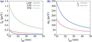
We calculate for GaAs QDs using . Results are plotted in Fig. 4. For nm, eV and eV, approving the parameters, and (representing and in the main text, since we consider only the piezoelectric electron-phonon coupling for transverse phonons there), chosen in the main text.
Appendix B Comparison between the Fermi-Golden Rule approximation and the Rate equation method
The Fermi Golden Rule approximation is valid when Jiang et al. (2012). Here we will examine situations in which the condition is relaxed. We assume that the broadenings of the QD levels are still much smaller than the thermal energy . The transport currents can then be calculated through Eq. (3). However, the particle current itself attains a more complex form in terms of the electrochemical potentials and temperatures. In this regime, the steady state distributions on the two QDs, and , can be calculated by solving the following rate equations in steady state,
| (22) | |||
| (23) |
Once obtaining and , the particle current can be calculated via
| (24) |
When , the Fermi Golden Rule approximation is validated, since and .
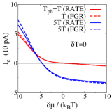
We plot - characteristics for different phonon temperatures using the rate equation method and the Fermi Golden Rule approximation in Fig. 5. It is noted that differences are negligible unless we operate in the far-from equilibrium regime, , or . Our results in Fig. 5 indicate that the nonlinear performance is marginally reduced; qualitative features remain the same. We speculate that the phenomena described in this work persist beyond the strict regimes where the rate equation method or the Fermi Golden Rule approximation are justifiable. Simulations in the main text of this paper were calculated using the rate equation method.
Appendix C Restrictions on the thermal transistor effect in the linear-response regime from the second-law of thermodynamics
Here we discuss restrictions, directly arising from the second-law of thermodynamics, on the thermal transistor effect which we materialize in the linear-response regime [see Fig. 3(a)]. Our discussion below is based on general irreversible thermodynamic arguments, and is holds for any thermodynamic systems in the linear response regime. Since our analysis here is confined to the thermal transistor effect, we shall consider pure thermal conduction (i.e., the electrochemical potential difference is set to zero).
For a system with three reservoirs, one can define three heat currents (one for each reservoir). However, due to energy conservation, , we are left with two independent heat currents Jiang et al. (2012); Jiang (2014b). If we choose the heat current flowing out of the source and that emerging from the phonon terminal as the two independent currents, the thermal transport equation for three terminal in the linear response regime can be generally written as,
| (31) |
Here is the heat current flowing out of the source. is the equilibrium temperature. and are the diagonal thermal conductance, while stands for the off-diagonal thermal conductance. The above equation is derived using Onsager’s theory of linear-response by finding the thermodynamic forces conjugated to the two heat currents. It can also be obtained by linearizing the transport equation in the main text, Eq. (6), and then reorganizing the transport coefficients according to the definition of . The second-law of thermodynamics imposes the following restrictions on transport coefficients,
| (32) |
We now note that in a three-terminal system, one can generally identify two distinct classes of transport mechanisms: (i) those involving only two terminals (reservoirs) in each microscopic process (briefed as “2T-class”); (ii) those in which energy is exchanged among three reservoirs in each transport process (briefed as “3T-class”).
For the 2T-class, the thermal transport equations in the linear response regime are generally given by,
| (33a) | |||
| (33b) | |||
| (33c) | |||
where , , and are the thermal conductances between pairs of reservoirs. The above equations represent Fourier’s law of thermal conduction. The second law of thermodynamics requires that the thermal conductances are positive,
| (34) |
We can organize equations (33) into the general form (31), written in terms of a new set of transport coefficients,
| (35) |
Based on the restrictions (34), we find that [on top of Eq. (32)],
| (36) |
As discussed in the main text, the heat current amplification factor in the linear response regime is given by
| (37) |
From Eq. (36) it is now clear that there is no thermal transistor effect for 2T-class models in the linear-response regime since they identically result in . (Recall, the 2T-class transport mechanisms correspond to a three terminal situation, with transport processes occurring independently between every pair of terminals. ) In contrast, for 3T-class transport mechanisms, the restriction (32) does not disallow heat current amplification, . In fact, as discovered in this work, one can manifest the thermal transistor effect in the linear response regime for the phonon-assisted hopping process, which is an example of the 3T-class transport mechanisms.
References
- Onsager (1931) L. Onsager, Phys. Rev. 37, 405 (1931).
- Jiang (2014a) J.-H. Jiang, Phys. Rev. E 90, 042126 (2014a).
- Dresselhaus et al. (2007) M. S. Dresselhaus et al., Adv. Mater. 19, 1043 (2007).
- Vineis et al. (2010) C. J. Vineis, A. Shakouri, A. Majumdar, and M. G. Kanatzidis, Adv. Mater. 22, 3970 (2010).
- Malen et al. (2010) J. Malen, S. Yee, A. Majumdar, and R. Segalman, Chem. Phys. Lett. 491, 109 (2010).
- Hochbaum and Yang (2010) A. I. Hochbaum and P. Yang, Chem. Rev. 110, 527 (2010).
- Dubi and Di Ventra (2011) Y. Dubi and M. Di Ventra, Rev. Mod. Phys. 83, 131 (2011).
- Shakouri (2011) A. Shakouri, Ann. Rev. Materials Research 41, 399 (2011).
- Sothmann et al. (2015) B. Sothmann, R. Sánchez, and A. N. Jordan, Nanotechnology 26, 032001 (2015).
- Vashaee and Shakouri (2004) D. Vashaee and A. Shakouri, Phys. Rev. Lett. 92, 106103 (2004).
- Zebarjadi et al. (2007) M. Zebarjadi, K. Esfarjani, and A. Shakouri, App. Phys. Lett. 91, 122104 (2007).
- Meair and Jacquod (2013) J. Meair and P. Jacquod, J. Phys.: Condens. Matter. 25, 082201 (2013).
- Leijnse et al. (2010) M. Leijnse, M. R. Wegewijs, and K. Flensberg, Phys. Rev. B 82, 045412 (2010).
- Sánchez and López (2013) D. Sánchez and R. López, Phys. Rev. Lett. 110, 026804 (2013).
- López and Sánchez (2013) R. López and D. Sánchez, Phys. Rev. B 88, 045129 (2013).
- Argüello-Luengo et al. (2015) J. Argüello-Luengo, D. Sánchez, and R. López, Phys. Rev. B 91, 165431 (2015).
- Hwang et al. (2015) S.-Y. Hwang, R. Lopez, and D. Sanchez, Phys. Rev. B 91, 104518 (2015).
- Svensson et al. (2013) S. F. Svensson et al., New J. Phys. 15, 105011 (2013).
- Whitney (2013a) R. S. Whitney, Phys. Rev. B 87, 115404 (2013a).
- Whitney (2013b) R. S. Whitney, Phys. Rev. B 88, 064302 (2013b).
- Kuo and Chang (2010) D. M.-T. Kuo and Y.-C. Chang, Phys. Rev. B 81, 205321 (2010).
- Azema et al. (2014) J. Azema, P. Lombardo, and A.-M. Daré, Phys. Rev. B 90, 205437 (2014).
- Henriet et al. (2015) L. Henriet, A. N. Jordan, and K. L. Hur, arXiv:1504.02073 (2015).
- Entin-Wohlman et al. (2010) O. Entin-Wohlman, Y. Imry, and A. Aharony, Phys. Rev. B 82, 115314 (2010).
- Jiang et al. (2012) J.-H. Jiang, O. Entin-Wohlman, and Y. Imry, Phys. Rev. B 85, 075412 (2012).
- Jiang et al. (2013) J.-H. Jiang, O. Entin-Wohlman, and Y. Imry, New J. Phys. 15, 075021 (2013).
- Jiang (2014b) J.-H. Jiang, J. Appl. Phys. 116, 194303 (2014b).
- Li et al. (2012) N. Li, J. Ren, L. Wang, G. Zhang, P. Hänggi, and B. Li, Rev. Mod. Phys. 84, 1045 (2012).
- Li et al. (2006) B. Li, L. Wang, and G. Casati, Appl. Phys. Lett. 88, 143501 (2006).
- Sánchez et al. (2010) R. Sánchez, R. López, D. Sánchez, and M. Büttiker, Phys. Rev. Lett. 104, 076801 (2010).
- Sothmann et al. (2012) B. Sothmann, R. Sánchez, A. N. Jordan, and M. Büttiker, Phys. Rev. B 85, 205301 (2012).
- Sothmann and Büttiker (2012) B. Sothmann and M. Büttiker, Europhys. Lett. 99, 27001 (2012).
- Rutten et al. (2009) B. Rutten, M. Esposito, and B. Cleuren, Phys. Rev. B 80, 235122 (2009).
- Juergens et al. (2013) S. Juergens, F. Haupt, M. Moskalets, and J. Splettstoesser, Phys. Rev. B 87, 245423 (2013).
- Torre et al. (2015) I. Torre, A. Tomadin, R. Krahne, V. Pellegrini, and M. Polini, Phys. Rev. B 91, 081402 (2015).
- Koch et al. (2004) J. Koch, F. von Oppen, Y. Oreg, and E. Sela, Phys. Rev. B 70, 195107 (2004).
- Segal (2005) D. Segal, Phys. Rev. B 72, 165426 (2005).
- Ren et al. (2012) J. Ren, J.-X. Zhu, J. E. Gubernatis, C. Wang, and B. Li, Phys. Rev. B 85, 155443 (2012).
- Kulkarni et al. (2014) M. Kulkarni, O. Cotlet, and H. E. Türeci, Phys. Rev. B 90, 125402 (2014).
- Thierschmann et al. (2015) H. Thierschmann, F. Arnold, M. Mittermüller, L. Maier, C. Heyn, W. Hansen, H. Buhmann, and L. W. Molenkamp, ArXiv e-prints (2015), eprint 1502.03021.
- Koch et al. (2014) T. Koch, J. Loos, and H. Fehske, Phys. Rev. B 89, 155133 (2014).
- Arrachea et al. (2014) L. Arrachea, N. Bode, and F. von Oppen, Phys. Rev. B 90, 125450 (2014).
- Zhou et al. (2015) H. Zhou, J. Thingna, J.-S. Wang, and B. Li, Phys. Rev. B 91, 045410 (2015).
- Simine et al. (2015) L. Simine, W. J. Chen, and D. Segal, J. Phys. Chem. C 119, 12097 (2015).
- Giazotto et al. (2006) F. Giazotto, T. T. Heikkilä, A. Luukanen, A. M. Savin, and J. P. Pekola, Rev. Mod. Phys. 78, 217 (2006).
- Fedichkin and Fedorov (2004) L. Fedichkin and A. Fedorov, Phys. Rev. A 69, 032311 (2004).
- Wu et al. (2005) Z.-J. Wu et al., Phys. Rev. B 71, 205323 (2005).
- Weber et al. (2010) C. Weber, A. Fuhrer, C. Fasth, G. Lindwall, L. Samuelson, and A. Wacker, Phys. Rev. Lett. 104, 036801 (2010).
- Andrieux and Gaspard (2004) D. Andrieux and P. Gaspard, J. Chem. Phys. 121, 6167 (2004).
- Jiang et al. (2015) J.-H. Jiang, M. Kulkarni, D. Segal, and Y. Imry, in preparation (2015).
- Saira et al. (2007) O.-P. Saira, M. Meschke, F. Giazotto, A. M. Savin, M. Möttönen, and J. P. Pekola, Phys. Rev. Lett. 99, 027203 (2007).
- Bauer et al. (2012) G. E. W. Bauer, E. Saitoh, and B. J. van Wees, Nature Materials 11, 391 (2012).
- Madelung (1987) O. Madelung, ed., Semiconductors, Landolt-Börnstein, New Series, Group III-V, vol. 17 (Springer, Berlin, 1987).