Metallic State of Low Mobility Silicon at High Carrier density induced by an Ionic Liquid
Abstract
High mobility and dilute two-dimensional electron systems exhibit metallic behavior down to the lowest experimental temperatures. In studies of ionic liquid gated insulating silicon, we have observed transitions to a metallic state in low mobility samples at much higher areal carrier densities than found for samples of high mobility. We have also observed a mobility peak in metallic samples as the carrier density was increased beyond .
It was initially believed that a metallic regime would not be found in two dimensional (2D) systems. As a function of carrier density there would only be a crossover from weak to strong localization.(Abrahams et al., 1979) This scenario was confirmed experimentally in highly disordered silicon systems almost 30 years ago, with no metallic state being found. As sample mobilities increased, metallic regimes were observed. In the case of n-type Si MOSFETs with mobility metallic behavior was found at .(Kravchenko et al., 1994) In n and p -type GaAs/AlGaAs quantum wells with , a transition was found at (Hanein et al., 1998; Dultz et al., 1998). There is currently a question as to whether these metal-insulator transitions (MITs) are crossovers or quantum phase transitions. (Das Sarma et al., 2014) A thorough review of the experiments can be found in Ref. Spivak et al., 2010. In addition to exhibiting 2D MITs, ⟨100⟩ Si has been shown to be superconducting with heavy B doping and ⟨111⟩ Si wafers have been shown to be superconducting with monolayers of Pb or In on the crystal surface.(Bustarret et al., 2006; Zhang et al., 2010) The search for superconductivity in Si using ionic liquid gating was the original motivation for this work.
With the use of ionic liquid gating, we have created 2D hole gases (2DHGs) on low mobility Si wafers. In this Letter we report both a transition to a metallic state with a critical sheet carrier density higher than previously reported and a peak in the mobility as a function of carrier density. A high carrier density metallic state, while unexpected, was predicted to exist by Das Sarma and Hwang.(Das Sarma and Hwang, 2014a) The goal of their theory was to determine a scaling relationship between the critical carrier density to observe metallic behavior and the peak mobility to explain the different critical carrier densities observed in MIT experiments. This was done by looking at the 2D conductivity using the Drude model in which it is determined by the product where is the Fermi wavevector and the mean free path. Boltzmann transport theory was used to determine the dependence of on carrier density and the Ioffe-Regel criteria () was used to determine the carrier density where a crossover to metallic behavior would be observed. In their theory the transition to a metallic state is not a phase transition but is a crossover.
Ionic liquids (ILs) such as N,N-diethyl-N-(2-methoxyethyl)-N-methylammonium bis(trifluoromethylsulphonyl-imide) (DEME-TFSI) have been used to study MITs and superconductor-insulator transitions by electrostatic charging because using them one can reach higher carrier concentrations than achievable with conventional capacitor configurations employing solid dielectrics.(Misra et al., 2007; Shimotani et al., 2007) Ionic liquids are in effect room temperature molten salts. They consist of mobile charged ions that will move to the electrode surfaces with an applied electric field. Electric double layers form at the positive and negative electrodes with the bulk liquid remaining in a neutrally charged state. These ion/electrode interfaces can be viewed as individual capacitors with nanometer level separation. High carrier concentrations are achievable without the limitations of leakage due to electron tunneling or dielectric breakdown characteristic of devices using thin dielectrics. Gating of oxides with an ionic liquid under certain conditions is also known to induce oxygen vacancies.(Jeong et al., 2013) The current understanding is that the process of inducing charge carriers with ionic liquid based transistors may involve both electrostatic and chemical processes with the balance between the two determined by voltage and temperature. Gating at low temperatures can inhibit electrochemical reactions, but gating must be performed at high enough temperatures that the ions remain mobile.
Samples were prepared from Si wafers grown by the Czochralski process. The numbers of oxygen inclusions are larger and the mobilities lower, with wafers grown this way, as compared with float-zone grown wafers.(Borghesi et al., 1995) The wafers were B doped and exhibited resistivities of . Silicon MOSFETs used to observe the MIT employed pn junctions to isolate the conductive channel from the bulk wafer. In the present work we induced additional holes onto the surface of a p-type Si wafer. Silicon exhibits an activated resistance as a function of temperature due thermal excitation of carriers above an energy gap. Conduction in a surface channel should become observable at temperatures below those at which the bulk carriers freeze out. The channel sheet resistance was determined using the van der Pauw method(Sup, ).
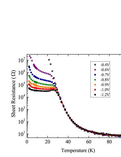
Trapped charges in the oxide coating can spontaneously form an inversion layer on a p-type Si wafer, and if such a layer were present, the 2K resistance could be as low as a M. While rare, this was observed in several samples, but the behavior was suppressed with the accumulation of holes on the surface. At 2K the resistance of the Si samples would be above the input impedance of the electronics unless a conductive surface layer were formed. When increasing the magnitude of the gate voltage, , we observe no change at high temperatures, which we attribute to the dominance of bulk conduction, but we do observe a decrease in the low temperature resistance from to k, as shown in Fig. 1. We have only been able to produce such a state by gating of ⟨100⟩ Si wafers. We could not do this using ⟨111⟩ Si wafers with a similar B doping level. The results are reminiscent of those of Ando et al. in which ions trapped within the layer were reported to form a 2D surface state in p-type Si.(Ando et al., 1982)
Carrier concentrations of samples were obtained in two different ways, from the Hall effect at low temperatures and by integrating the current flowing to the gate during charging. The carrier concentrations in Fig. 2 were determined using the latter procedure. The carrier density produced by the integration method is also a measure of the number of excess anions that moved to the surface. In this approach there is a nonzero leakage current that needs to be accounted for, and this was done by subtracting off the value of the current in the long time limit. The subtracted term was at the level of, or below a nA, and lead to a small change in the integrated area. Integration resulted in carrier densities within a factor of order unity to those obtained from the Hall number. This method can fail at higher voltages where the leakage current is large and does not asympototicly decay. When oxidation of the electrode occurs, the integrated carrier density can be a factor of 10 higher than that of the Hall carrier density.(Petach et al., 2014) Our experiments were designed to minimize oxidation processes.(Sup, )
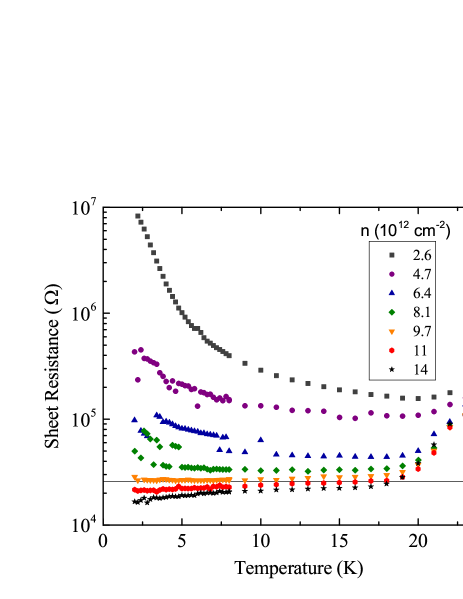
The Hall effect was measured at for some samples and from the Hall number, and when the sheet resistance, . Many samples exhibited measurable conduction at low temperatures but only a few showed metallic behavior. Samples that exhibited metallic behavior remained metallic down to 450mK. This was the lowest accessible temperature. The resistance vs. temperature of the insulating state at low hole concentrations was Arrhenius activated, and it transitioned to a regime in which at higher hole concentrations as the metallic regime was approached.
An example of a sample that showed metallic behavior is plotted in Fig. 2. The data were collected by warming the sample and the lowest measured temperature was 2K. High mobility silicon MOSFETs exhibited a transition to a metallic state at a resistance of . The present samples exhibited a transition at , a value also reported by Zataritskaya and Zavaritskaya for p-type and n-type Si inversion layers.(Zavaritskaya and Zavaritskaya, 1987)
Ionic liquid gating of Si was determined to be reversible without hysteresis across the MIT.(Sup, ) This is in contrast with the MIT observed in where the samples remained metallic when the negative gate voltage was removed.(Jeong et al., 2013) Oxidation of the sample was believed to be the source of the hysteresis in the experiment. In addition, a chemical reaction, if it occurred reversibly, would happen at the interface between the ionic liquid and the silicon oxide, whereas the conductive channel is a distance away, spatially separated by the thickness of the oxide.
Das Sarma and Hwang predicted that the carrier density, , at the initial transition to metallic behavior would scale with the inverse of the peak mobility.(Das Sarma and Hwang, 2014a) For the values of the mobilities of the wafers of the present work, they would predict that ; however, it was believed that such systems would be too disordered for a metallic state to exist.(Das Sarma and Hwang, 2014a)
The observation of a transition to a metallic state in low mobility devices was unexpected, as previous findings all involved high mobility samples. An open question remains as to whether the high carrier density, low mobility metallic state is similar to the low carrier density high mobility state studied by others and whether the transition from the insulating to metallic state is a quantum phase transition or a crossover. At present we have no answer to these questions. Long range interactions dominate at the carrier densities of previous experiments whereas the low mobility transition occurs at a carrier concentration where short range interactions should be an important factor.
A measure of the importance of long-range interactions is the dimensionless parameter where is the Bohr radius. This parameter is the ratio of the Coulomb energy to the Fermi energy. For dilute 2D systems, is typically high at the critical carrier density for the MIT. Using the bulk parameters for Si we calculate for the heavy hole band. This suggests that the metallic regime of these ionic liquid gated systems could be different from those of MOSFETs. However a calculation using Si band parameters might not be the whole story. In MOSFETs the metallic gates must be far enough away from the channel to suppress electron tunneling from the gate. With ionic liquid gating, the ions sit on the oxide surface from the 2D electron gas. We cannot rule out the possibility that the ions produce a strong spatially varying electric field that the carriers in the conductive channel experience. The interaction of accumulated holes with this potential could lead to an increase in the hole effective mass, a decrease in , and thus an increase in from the values calculated from silicon band parameters.
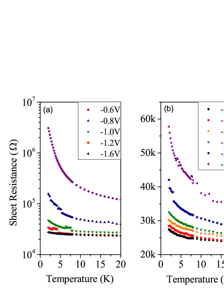
Previous experiments on low mobility samples at very high carrier density observed that electron mobility decreased with increasing carrier density and there was no metallic regime.(Ando et al., 1982) The decrease in carrier mobility is typically associated with either surface surface roughness or scattering from trapped charges in the oxide. Similar observations have been made with electrolyte gated rubrene samples where the decrease in mobility was thought to be due to electrostatic disorder produced by the ions.(Xie et al., 2014) A peak in the mobility as a function of carrier density was also observed in the Si surface layer presented here. A typical result is plotted in Fig. 3, where the sample became less insulating with increasing carrier density at low carrier densities and more insulating at higher carrier densities, implying the existence of a peak in the mobility at a carrier density of the order of as measured by the Hall effect. Wei et al. have reported a similar peak in gated rubrene at similar carrier densities.(Xie et al., 2014) In addition, the data such as that of Fig 3 were repeatable when the sample was removed from the system and attached to a low temperature insert for a subsequent run. Other samples were similarly reproducible and this suggests that degradation of the sample is not an explanation of the high carrier density behavior. In contrast with Fig. 2, metallic behavior was not observed in the sample plotted in Fig. 3. Metallic samples also show a peak in the mobility as a function of carrier density.
We can rule out the mobility peak being an electrochemical effect. The surface oxide passivation layer reduces the trap density on the Si surface from upwards of to values as low as in addition to serving as an insulating barrier between the ions and conducting channel.(Cobbold, 1970) The carrier density as a function of gate voltage is linear through the conductance peak consistent with electrostatic rather than electrochemical behavior. Further support for electrostatic behavior is the fact that the capacitance calculated from vs from Fig. 4 agrees with the capacitance expected from a thick capacitor. The gate voltages used are also within the electrochemical window of DEME-TFSI and so an electrochemical reaction is unlikely.(Yuan et al., 2009) The electrochemical window sets an upper limit to the voltage that when exceeded results in breakdown of the electrolyte.(Ong et al., 2011)
At high carrier densities, short range interactions dominate the scattering time as opposed to long range iterations. Das Sarma and Hwang calculated the scattering time due to surface roughness of the oxide interface, which is a source of short range disorder, and found that the mobility would decrease as the sheet carrier density exceeded . The calculation was done to explain the observed mobility peak in low mobility Si samples. In addition they proposed that for high mobility Si MOSFETs at sheet carrier densities of around the mobility would be reduced sufficiently such that and the system would undergo a second MIT and reenter the insulating state.(Das Sarma and Hwang, 2014b)
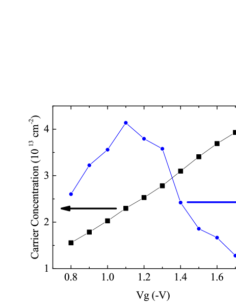
Thus there would be two critical carrier densities, and Metallic behavior would be observed when . The most likely value for the carrier density of the second transition would be .(Das Sarma and Hwang, 2014b) Figure 4 shows the mobility calculated from the conductivity at 2K along with the carrier density as a function of gate voltage. For this sample, from to and in this range the conductivity appears to increase with decreasing temperature. It is worth noting that the sample plotted in Fig. 4 was not as strongly metallic as the samples presented in Fig. 2 or in Fig. 2 of the supplemental material, but those samples where not pushed into the insulating state by further increase of the carrier density. A more conclusive result would be to observe reentrant behavior in a more strongly metallic sample while increasing carrier densities to drive the sample much further into the insulating state.
The origin of why we see metallic behavior in a subset of samples is also an open question. If the peak wafer mobility were to lead to it would then appear possible that there would be no metallic state. This could explain why a metallic regime is not seen in every sample. Another open question is why there is a metallic regime in samples whose mobilities are well below those of Ref. Ando et al., 1982 for which a MIT was not observed. At very high carrier densities screening of Coulomb disorder may play a role and as a result the observed metallic state may not involve the same physics as the ones previously seen.
In summary, ionic liquid gating has been used to induce holes on the surface of p-type ⟨100⟩ Si wafers. The contacts were also p-type and the samples were cooled down to freeze out the bulk carriers and thus permit the measurement of the induced surface conducting channel. The low temperature Hall mobilities were on the order of and not as seen in Si MOSFETs that undergo a MIT. In the low mobility samples, a MIT was found with a value much higher than that found in all previous studies of the MIT. It is generally believed that a metallic state would be unlikely at such a high level of disorder. In addition it was found that above both metallic and insulating samples become more insulating with increasing carrier concentration. Finally the mobility at peak conductance was higher than the mobility peak in rubrene gated with an ionic liquid.(Xie et al., 2014)
Acknowledgements.
This work was supported in part by NSF/DMR-1263316. Devices were fabricated at the Minnesota Nanofabrication Center which receives partial support from the NSF through the NNIN program. They were characterized at the University of Minnesota Characterization Facility, a member of the NSF-funded Materials Research Facilities Network via the MRSEC program. The authors would like to thank Boris Shklovskii for useful discussions.References
- Abrahams et al. (1979) E. Abrahams, P. W. Anderson, D. C. Licciardello, and T. V. Ramakrishnan, Phys. Rev. Lett. 42, 673 (1979).
- Kravchenko et al. (1994) S. V. Kravchenko, G. V. Kravchenko, J. E. Furneaux, V. M. Pudalov, and M. D’Iorio, Phys. Rev. B 50, 8039 (1994).
- Hanein et al. (1998) Y. Hanein, U. Meirav, D. Shahar, C. C. Li, D. C. Tsui, and H. Shtrikman, Phys. Rev. Lett. 80, 1288 (1998).
- Dultz et al. (1998) S. C. Dultz, H. W. Jiang, and W. J. Schaff, Phys. Rev. B 58, R7532 (1998).
- Das Sarma et al. (2014) S. Das Sarma, E. H. Hwang, K. Kechedzhi, and L. A. Tracy, Phys. Rev. B 90, 125410 (2014).
- Spivak et al. (2010) B. Spivak, S. V. Kravchenko, S. A. Kivelson, and X. P. A. Gao, Rev. Mod. Phys. 82, 1743 (2010).
- Bustarret et al. (2006) E. Bustarret, C. Marcenat, P. Achatz, J. Kacmarcik, F. Levy, A. Huxley, L. Ortega, E. Bourgeois, X. Blase, D. Debarre, and J. Boulmer, Nature 444, 465 (2006).
- Zhang et al. (2010) T. Zhang, P. Cheng, W.-J. Li, Y.-J. Sun, G. Wang, X.-G. Zhu, K. He, L. Wang, X. Ma, X. Chen, Y. Wang, Y. Liu, H.-Q. Lin, J.-F. Jia, and Q.-K. Xue, Nat Phys 6, 104 (2010).
- Das Sarma and Hwang (2014a) S. Das Sarma and E. H. Hwang, Phys. Rev. B 89, 235423 (2014a).
- Misra et al. (2007) R. Misra, M. McCarthy, and A. F. Hebard, Applied Physics Letters 90, 052905 (2007).
- Shimotani et al. (2007) H. Shimotani, H. Asanuma, A. Tsukazaki, A. Ohtomo, M. Kawasaki, and Y. Iwasa, Applied Physics Letters 91, 082106 (2007).
- Jeong et al. (2013) J. Jeong, N. Aetukuri, T. Graf, T. D. Schladt, M. G. Samant, and S. S. P. Parkin, Science 339, 1402 (2013).
- Borghesi et al. (1995) A. Borghesi, B. Pivac, A. Sassella, and A. Stella, Journal of Applied Physics 77, 4169 (1995).
- (14) See Supplemental Material at [URL will be inserted by publisher].
- Ando et al. (1982) T. Ando, A. B. Fowler, and F. Stern, Rev. Mod. Phys. 54, 437 (1982).
- Petach et al. (2014) T. A. Petach, M. Lee, R. C. Davis, A. Mehta, and D. Goldhaber-Gordon, Phys. Rev. B 90, 081108 (2014).
- Zavaritskaya and Zavaritskaya (1987) T. N. Zavaritskaya and E. I. Zavaritskaya, JETP Letters 45, 609 (1987).
- Xie et al. (2014) W. Xie, S. Wang, X. Zhang, C. Leighton, and C. D. Frisbie, Phys. Rev. Lett. 113, 246602 (2014).
- Cobbold (1970) R. Cobbold, Theory and applications of field-effect transistors (Wiley-Interscience, 1970).
- Yuan et al. (2009) H. Yuan, H. Shimotani, A. Tsukazaki, A. Ohtomo, M. Kawasaki, and Y. Iwasa, Advanced Functional Materials 19, 1046 (2009).
- Ong et al. (2011) S. P. Ong, O. Andreussi, Y. Wu, N. Marzari, and G. Ceder, Chemistry of Materials 23, 2979 (2011), http://dx.doi.org/10.1021/cm200679y .
- Das Sarma and Hwang (2014b) S. Das Sarma and E. H. Hwang, Phys. Rev. B 89, 121413 (2014b).