Exploring Packaging Strategies of Nano-embedded Thermoelectric Generators
Abstract
Embedding nanostructures within a bulk matrix is an important practical approach towards the electronic engineering of high performance thermoelectric systems. For power generation applications, it ideally combines the efficiency benefit offered by low dimensional systems along with the high power output advantage offered by bulk systems. In this work, we uncover a few crucial details about how to embed nanowires and nanoflakes in a bulk matrix so that an overall advantage over pure bulk may be achieved. First and foremost, we point out that a performance degradation with respect to bulk is inevitable as the nanostructure transitions to being multi moded. It is then shown that a nano embedded system of suitable cross-section offers a power density advantage over a wide range of efficiencies at higher packing fractions, and this range gradually narrows down to the high efficiency regime, as the packing fraction is reduced. Finally, we introduce a metric - the advantage factor, to elucidate quantitatively, the enhancement in the power density offered via nano-embedding at a given efficiency. In the end, we explore the maximum effective width of nano-embedding which serves as a reference in designing generators in the efficiency range of interest.
I Introduction
Low dimensional systems such as nanowires or nanoflakes are potential candidates for high performance thermoelectric systems with the likely enhancement in their electronic figure of merit Hicks and Dresselhaus (1993a, b); Snider and Toberer (2008); Dresselhaus et al. (2007) and hence the maximum thermodynamic efficiency, which is attributed to a distortion in their electronic density of states Heremans et al. (2008). However low-dimensional systems operate at much lower power outputs in comparison to their bulk counterparts. Bulk systems, on the other hand, offer much higher power densities for practical considerations, but at much lower efficiencies. Therefore, it is essential to beat this so called power-efficiency trade-off Muralidharan and Grifoni (2012); Nakpathomkun et al. (2010) by intelligently designing nano-structured bulk systems Heremans et al. (2008); Sothmann et al. (2013); Agarwal and Muralidharan (2014) aimed at combining the efficiency benefit of nano structuring with the power density advantage of bulk.
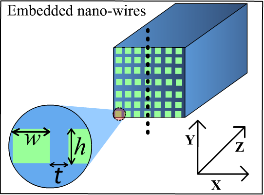
Approaches toward nano-structuring so far have proven successful in the suppression of phonon mediated heat flow Mingo and Broido (2004); Mingo (2004); Zhou et al. (2007, 2010); Boukai et al. (2008a); Hochbaum et al. (2008a); Poudel et al. (2008), while electronic engineering based on the DOS Goldsmid (2009); DiSalvo (1999); Shakouri (2011) of low-dimensional systems Giazotto et al. (2006); Muhonen et al. (2012); Paulsson and Datta (2003); Reddy et al. (2007) is still a topic of current and active research. One possible approach for electronic engineering is to pack low-dimensional systems in a bulk matrix Nakpathomkun et al. (2010); Kim et al. (2009); Yang et al. (2005) as shown in the schematic in Fig. 1(a) and (b), such that the efficiency benefit of nano structuring is tapped along the transport direction and the power advantage of bulk is harnessed via the areal packaging strategy Agarwal and Muralidharan (2014). With advancements in fabrication and lithographic procedures, atomic layers can be placed with the precision of the order of atomic dimensions Fuechsle et al. (2012), and hence it is envisionable that such packaging strategies are quite possible within the current experimental capabilities. Also, with tremendous progress in oxide based nanoelectronics, it may also be possible to engineer the desired barrier profile on demand Cen et al. (2009).
The key object of this paper is to analyze the packing strategies of such nano-embedded bulk systems and explore under what operating conditions do they offer advantages over traditional bulk thermoelectric generators. Specifically, we consider nanowire and nanoflake-embedded bulk systems, as depicted in Fig. 1(a) and (b), where the nano structure concerned is packed in between sufficiently thick barriers, as shown in the sample cross-sectional band profile depicted in Fig. 1(c). An analysis of packing strategies concerns a judicious choice of the barriers between the nano-structures and its relationship with the effective power density at a given operating efficiency to be discussed in depth here.
Traditionally, electronic engineering of low dimensional thermoelectrics concerns the optimization of the electronic figure of merit defined by
| (1) |
with , and being the Seebeck coefficient, electrical conductivity and electronic thermal conductivity respectively, and is the operating temperature.
While low dimensional systems definitely offer the advantage in terms of an enhanced figure of merit, it is now increasingly clear that one has to consider the power-efficiency trade-off Muralidharan and Grifoni (2012); Whitney (2014); Nakpathomkun et al. (2010) for a more complete design strategy. The most glaring example of the power-efficiency trade-off is the Sofo-Mahan thermoelectric Mahan and Sofo (1996), which features an infinite electronic figure of merit, but zero power output Muralidharan and Grifoni (2012); Whitney (2014); Humphrey and Linke (2005). That being said, is not an accurate measure of efficiency when power output is of the order of the quantum bound which is the maximum power any thermoelectric generator can produce Whitney (2014), Esposito et al. (2009a), Esposito et al. (2009b), Esposito et al. (2010). So, in this paper we primarily focus on the power density versus efficiency trade-off in embedded nano-systems.
A few crucial and fundamental aspects of electron engineering via nano-embedding are pointed out in this work. First and foremost, we show that a performance degradation is inevitable as the nano structure transitions to being multi moded, a trend which has been noted in a few experiments Hochbaum et al. (2008a). Turning to packing strategies, we point out that at higher packing fractions, judicious nano-embedding offers a significant power density advantage when operated over a large range of efficiencies. However, at lower packing fractions, this range gradually narrows down to the high efficiency regime. Finally, we introduce a metric - the advantage factor, to elucidate quantitatively, the enhancement in the power density offered via nano-embedding at a given efficiency. At the end, we explore the maximum effective width of nano-embedding which serves as a reference in designing nano-embedded generators in the efficiency range of interest.
II Model Details
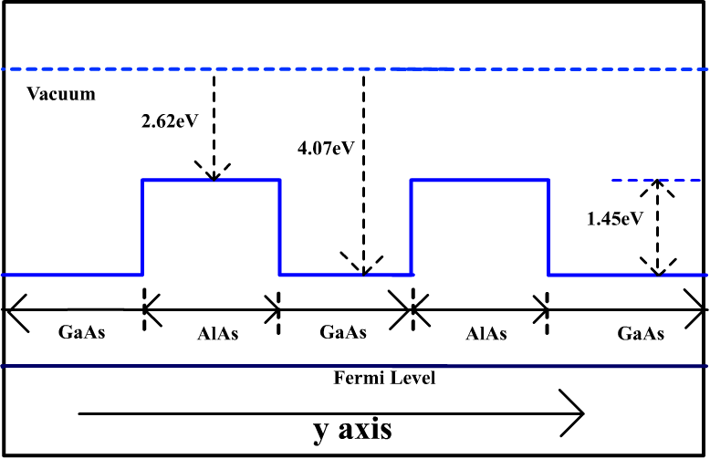
We model nano-embedded systems as quantum wires/flakes separated by energy barriers as shown in Fig. 1(a) and (b). For the purpose of our calculation, we use the parameters of lightly doped GaAs conducting channels and AlAs potential barriers to separate two GaAs conducting channels. AlAs serves as a potential candidate for energy barrier fabrication because GaAs and AlAs have approximately same lattice constant resulting in minimization of lattice strain due to lattice constant mismatch Streetman (1995). We start our calculations with nano devices of cross-sectional dimension embedded in a 3-D bulk matrix. The electron affinity of GaAs and AlAs are and respectively. According to Anderson’s rule Streetman (1995), an energy barrier of in a GaAs/AlAs system is feasible if the two materials are doped in a way such that their work-functions are equal. Further manipulation of the doping concentration of these materials results in higher energy barriers. The conduction band minima of the GaAs/AlAs system, given equal work-functions, are schematically depicted in Fig. 1(c). For our discussions we will simply assume that Anderson’s rule is valid and neglect complicated realistic variations in band offsets. A more practical DFT based calculation of band offsets in GaAs/AlAs junctions is depicted in Ribeiro, M. et al. (2011); Wang et al. (2013).
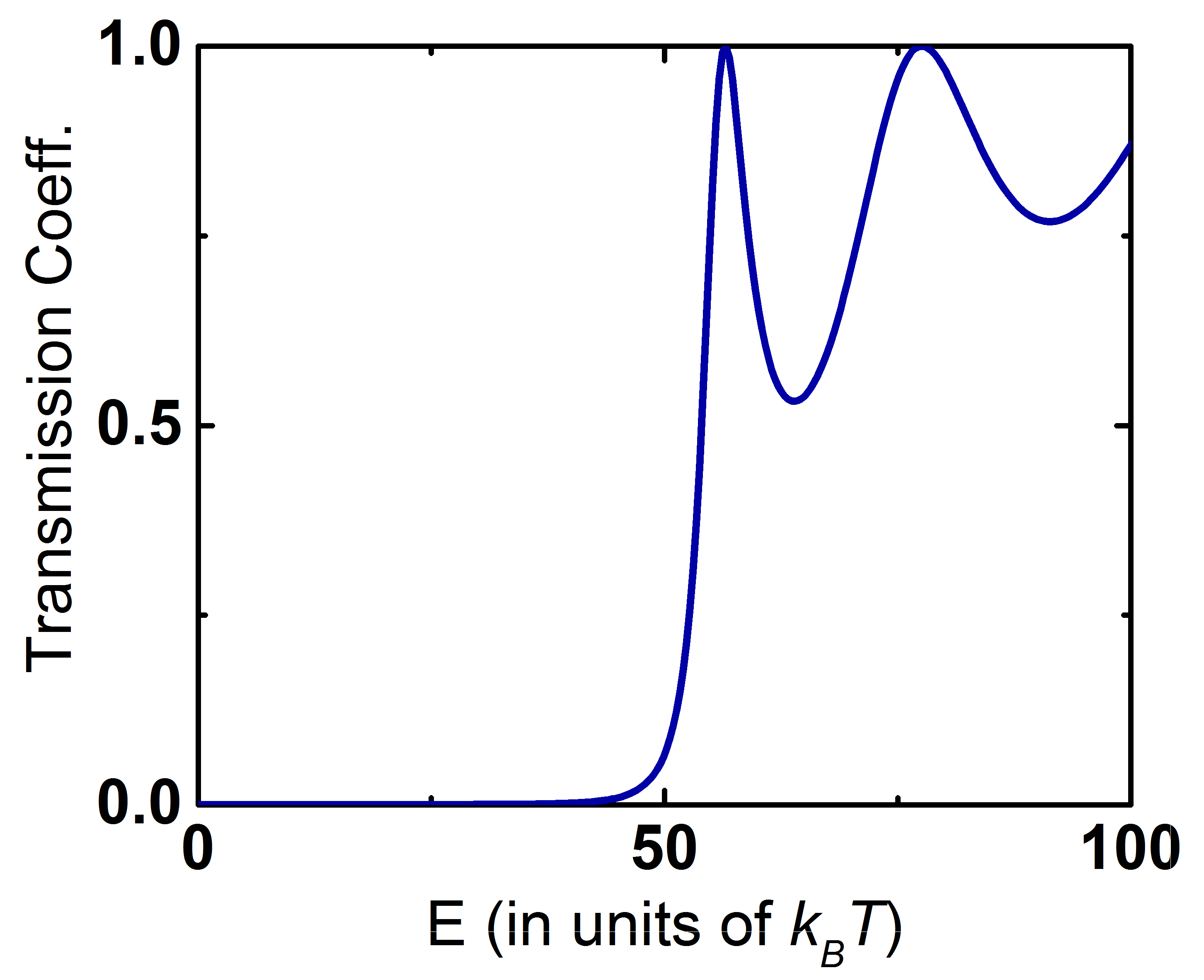
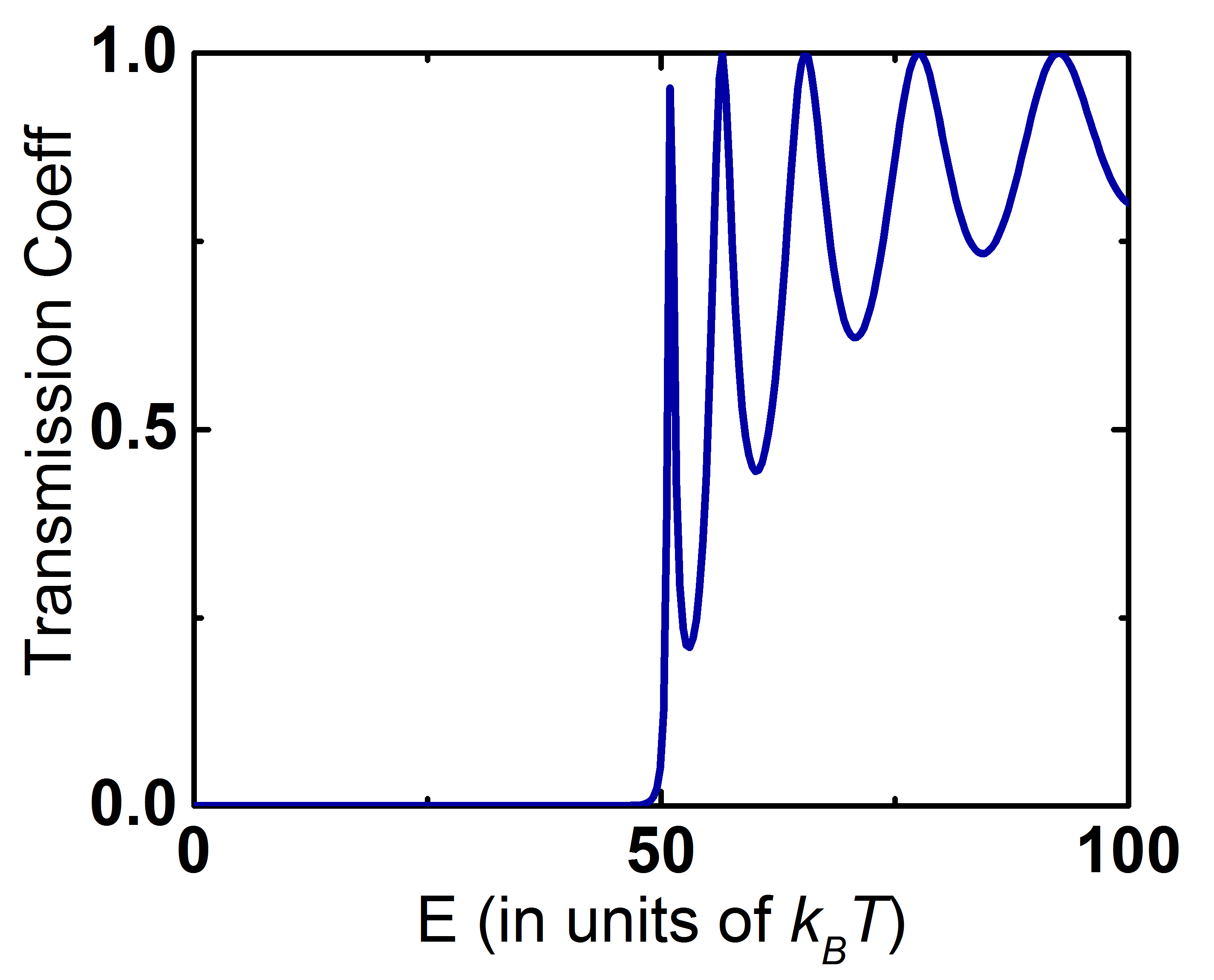
The ability of a 5nm AlAs barrier to suppress electronic transmission between two adjacent GaAs conducting channels is depicted in Fig. 2(a). The vanishing values of the transmission coefficient along the direction over a specific energy range implies an absence of electronic coupling between adjacent GaAs channels in that energy range. The transmission coefficient is calculated in ballistic limit using the non-equilibrium Green’s function (NEGF) formalism with an atomistic tight-binding Hamiltonian Datta (2005); Agarwal and Muralidharan (2014). It is clearly seen from Fig. 2(a) that a AlAs energy barrier of can suppress electronic transmission between adjacent GaAs channels upto at where is the kinetic energy of electrons. Fig. 2(b) demonstrates that a AlAs energy barrier is only marginally advantageous over a AlAs barrier in inhibiting electronic coupling below a kinetic energy of . We therefore conclude that is an optimum separation between two adjacent GaAs conducting channels in a GaAs/AlAs system.
We consider ballistic thermoelectric generators with electron transport in the direction such that Datta (2005); Agarwal and Muralidharan (2014). The charge and heat current through a device is given by Datta (2005)
| (2) |
| (3) |
where is the charge current, is the heat current, is the kinetic energy along the transport direction, is the minimum kinetic energy of sub-band, is the electron occupancy probability at the hot/cold contacts given by the respective Fermi-Dirac distributions kept at electrochemical potentials . The summation in (2) and (3) extends over all conducting sub-bands.
In the subsequent calculations, the temperatures of the hot and cold contacts, labeled and , are assumed to be and respectively. For simplicity, we assume parabolic dispersion relationship with a constant effective mass . To make calculations simple, we assume that both the contacts are perfectly symmetric and the doping of the GaAs conducting channel is uniform and that the voltage drops linearly across the GaAs channels. Assuming that the contacts are in local equilibrium, the quasi-Fermi levels in the contacts is given by where is the voltage dropped across the thermoelectric generator due to current flow through an external circuit and is the equilibrium electrochemical potential across the entire device.
To generate the power density vs efficiency plots in the next section, we use a voltage controlled model Muralidharan and Grifoni (2012); Agarwal and Muralidharan (2014) in order to vary the bias voltage across the thermoelectric generator. The power density and efficiency () are calculated for each value of the bias voltage (). The set of points comprising the power density and efficiency then constitute the curves in the plane for a particular .
With the above description in mind, we now turn our attention to the power density-efficiency trade-off in three types of embedded nano systems in the absence of electron-phonon interaction (ballistic limit) and phonon mediated heat flow- (1) A single moded nanowire of cross-section (2) A 2-D nanoflake of width (3) A multi moded nanowire () packed in a matrix.
III Nanostructures versus Bulk
Single moded nanowires: Our calculations use a single moded nanowire of length less than the mean free path of electrons so that electronic transport occurs predominantly in the ballistic regime. For simplicity, we assume that the electron wavefunction is confined only within the GaAs conducting channels. The kinetic energy of the electrons with respect to the conduction band minimum is given by
| (4) |
where is the minimum energy of the sub-band and is the conduction band effective mass of the electrons in GaAs.
A nanowire exhibits single moded property when the thermal broadening of the Fermi-Dirac distribution function is much less than the minimum energy separation between two sub-bands. Assuming that the separation between two sub-bands must be greater than , we deduce that the maximum cross-sectional dimensions that preserves the single moded property of a GaAs nanowire is approximately . We also note that the maximum cross-sectional dimension depends on the effective mass of the electrons. For example, for , redoing the above calculation gives .
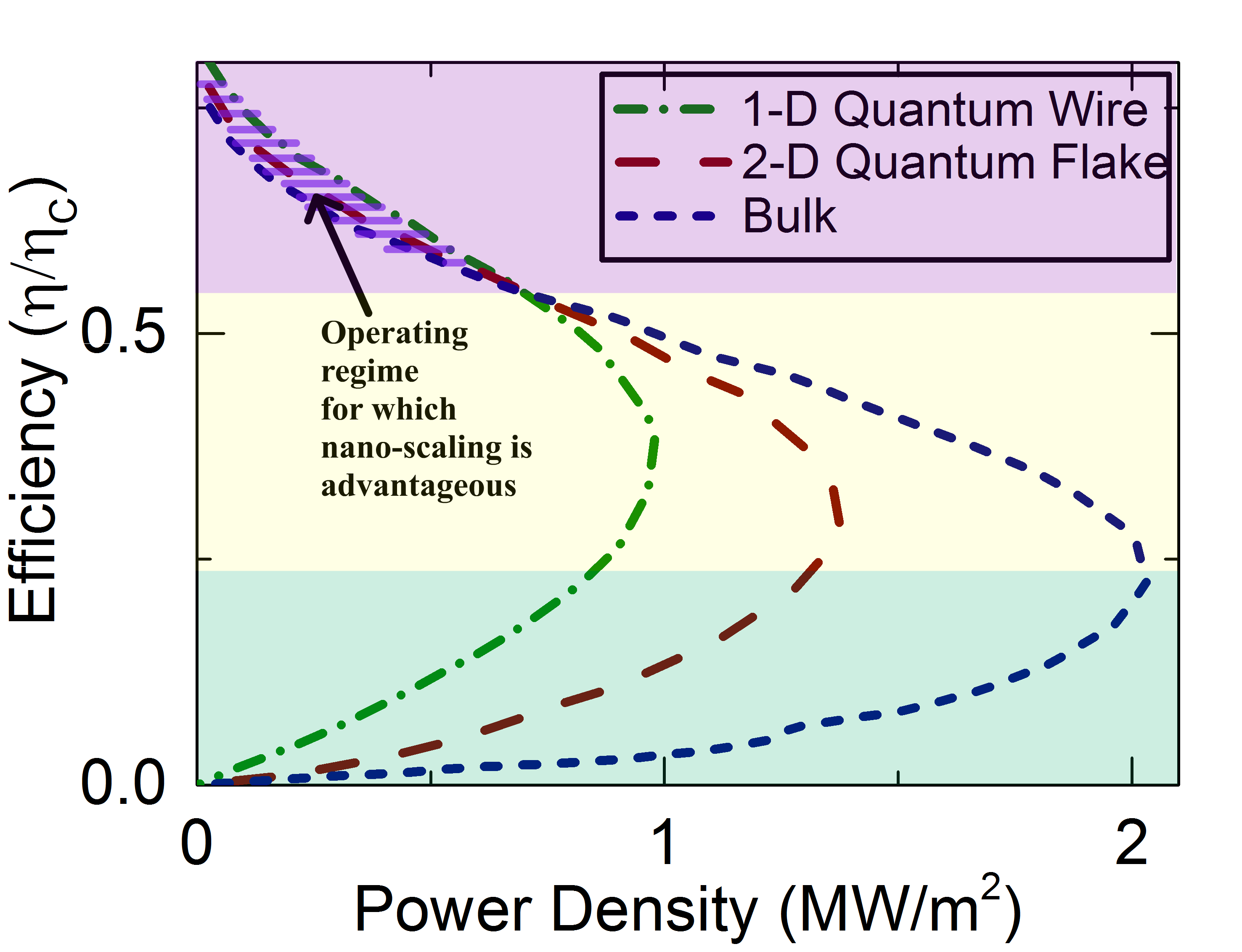
Although our calculations show that a nanowire remains single moded for , the true potential of nanowire generators is harnessed at . This is because the total power generated by the single moded nanowire does not change with area making the power density inversely proportional to the cross-sectional area. The power efficiency trade-off for a nanowire is shown in Fig. 3(a). For comparison, power-efficiency plot of a bulk thermoelectric generator is also shown in Fig. 3(d). We note that the maximum power density of a single moded quantum wire of cross-sectional dimensions is approximately , while that of a bulk generator is of the order of . Such high power density is expected given that the maximum power produced by a single moded nanowire is of the order of Kim et al. (2009).
Nanoflakes: As in the previous case, we consider a nanoflake of length
less than the mean free path of the electrons such that electronic transport is ballistic. Assuming that the transport is in the direction and the electronic confinement is in the direction, the kinetic energy of the itinerant electrons is given by:
| (5) |
where is the minimum energy of the sub-band due to electronic confinement and is the effective mass of the conduction band electrons in GaAs.
Purely two-dimensional electronic band properties are imposed on the nanoflakes when the thermal broadening of the Fermi function () is much less than the minimum energy separation between two sub-bands. Assuming that the separation between two sub-bands must be greater than at, we get .
Similar to a single moded nanowire, the power output of a nanoflake with only one conducting sub-band does not change with the width of the nanoflake. In terms of power density, a nanoflake with the smallest possible width is the most advantageous. Fig. 3(b) shows the power-density versus efficiency plot of a wide nanoflake. The maximum power density of a nanoflake of width is around , while a bulk generator provides a maximum power density of .
Multi moded nanowires: Next, we consider a nanowire with discrete sub-bands such
that energy separation between the lower modes is of the order of thermal broadening of the Fermi-Dirac distribution function (). Fig. 3(c) shows the power-efficiency trade-off in this case. It can be seen in comparing Figs. 3(a), (b), (c) and (d) that a nanowire
with multiple modes provides a lower performance not only
in power density but also in efficiency compared to the single moded nanowire, nanoflake and bulk thermoelectric generator.
A single moded nanowire operates at a higher efficiency at maximum power density compared to a multi moded nanowire. Multiple conducting sub-bands provide a number of higher energy levels for electron transport. Electronic flow through these higher energy levels from the hot contact to the cold contact results in higher electronic heat conductivity thereby reducing the efficiency of the thermoelectric generator. Also positioning the Fermi level near the higher energy sub-bands may result in significant back flow of electrons from the cold contact to the hot contact through the lower energy sub-band (hole like conduction) thereby reducing the power output and the voltage obtained at a given efficiency.
By comparing Figs. 3(a),(b),(c) and (d), we can infer that single moded nanowires and nanoflakes offer the possibility for a power density advantage, and hence may be engineered for an enhancement in the performance via nano-embedding as opposed to multi moded nanowires. So, we conclude that there is a maximum cross-sectional dimension beyond which the performance of a nanowire may degrade below the bulk performance, which is what we will consider next.
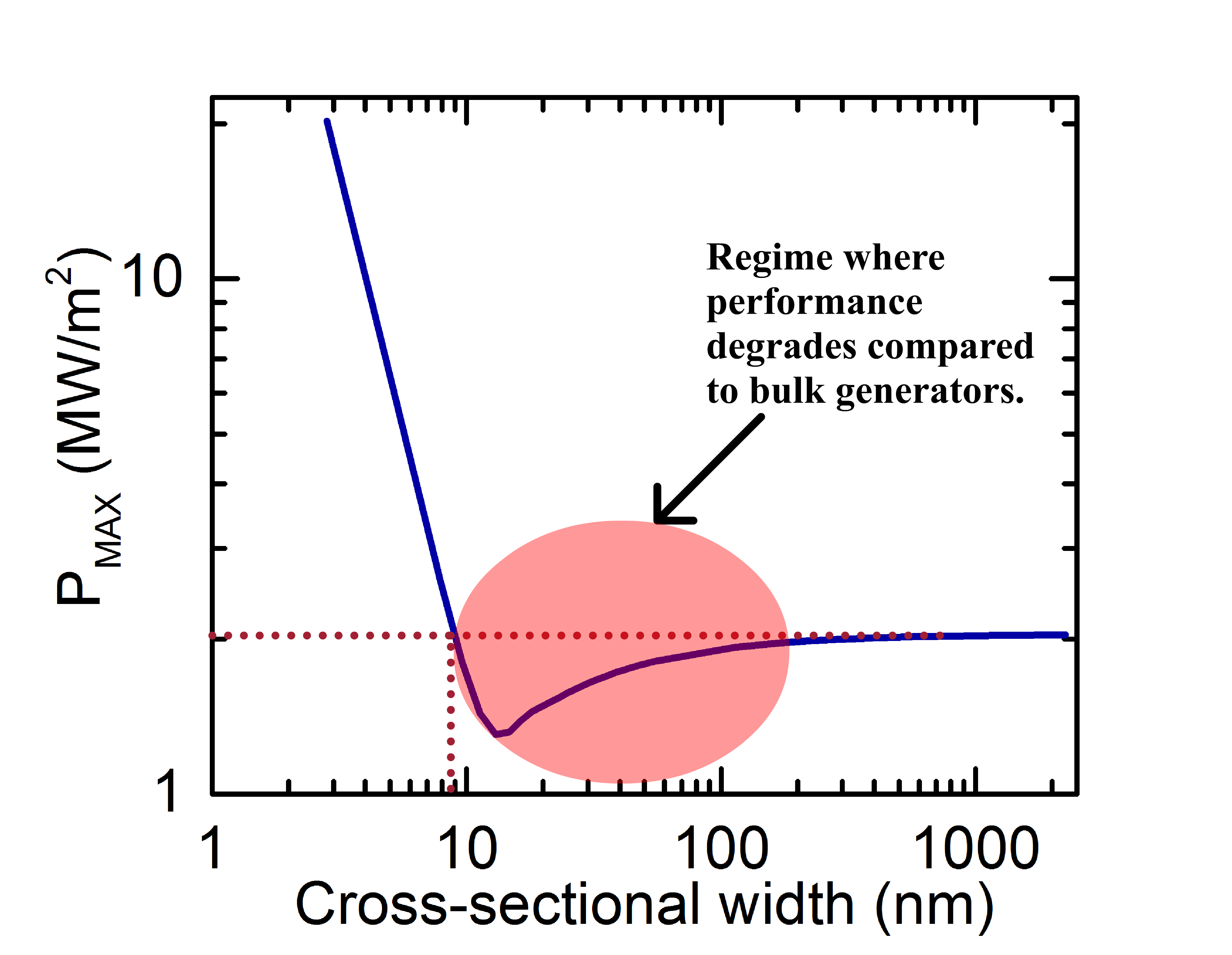
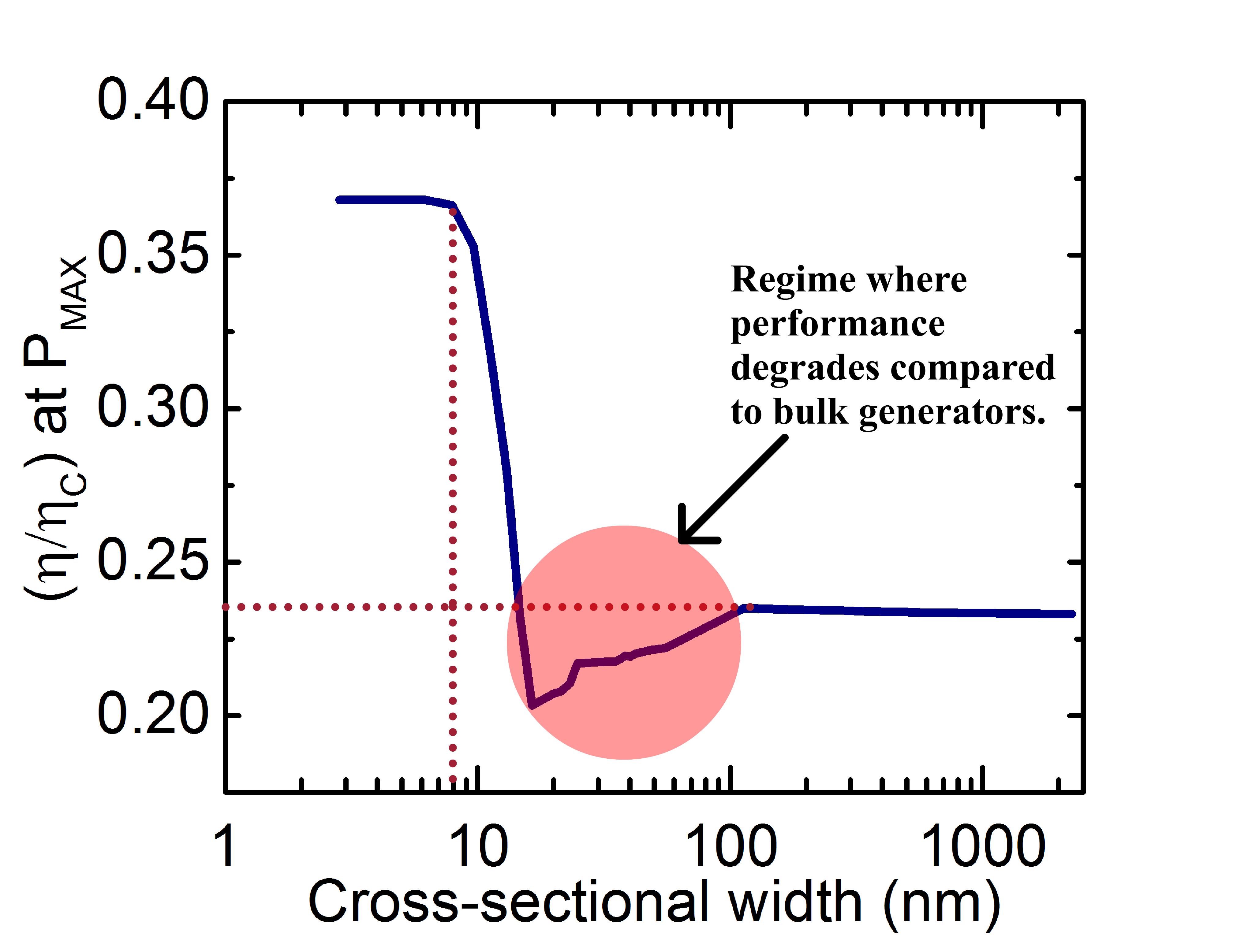
Single moded nanowire to bulk transition: The maximum cross-sectional width for which nanowires retain single moded electronic properties from the perspective of power generation is of particular interest in designing thermoelectric generators. For large cross-sectional dimension of the nanowire in comparison with the lattice constant, the separation between two sub-bands becomes much less than , and the nanowire begins to show bulk properties. Two quantities of interest which can be used to distinguish between lower dimensional and bulk thermoelectric generators are maximum power density () and the efficiency at maximum power density ().
In Figs. 4(a) and (b), we show that the advantages of single moded nanowires may be harnessed for , where the logarithm of the power density decreases linearly and the efficiency at maximum power () remains almost constant with the logarithm of the cross-sectional dimensions. Between , it behaves as a multi moded nanowire where the difference between two sub-bands is of the order of . For the nanowire behaves as a bulk material depicting the expected trend of constant power-density. As stated previously, the performance of a nanowire in the multi moded regime degrades in terms of both the maximum power density as seen in Fig. 4(a) as well as the efficiency as seen in Fig. 4(b) in comparison to single moded nanowire and bulk thermoelectric generators. A multi moded nanowire hence shows no promise in applications to nano-embedded systems.
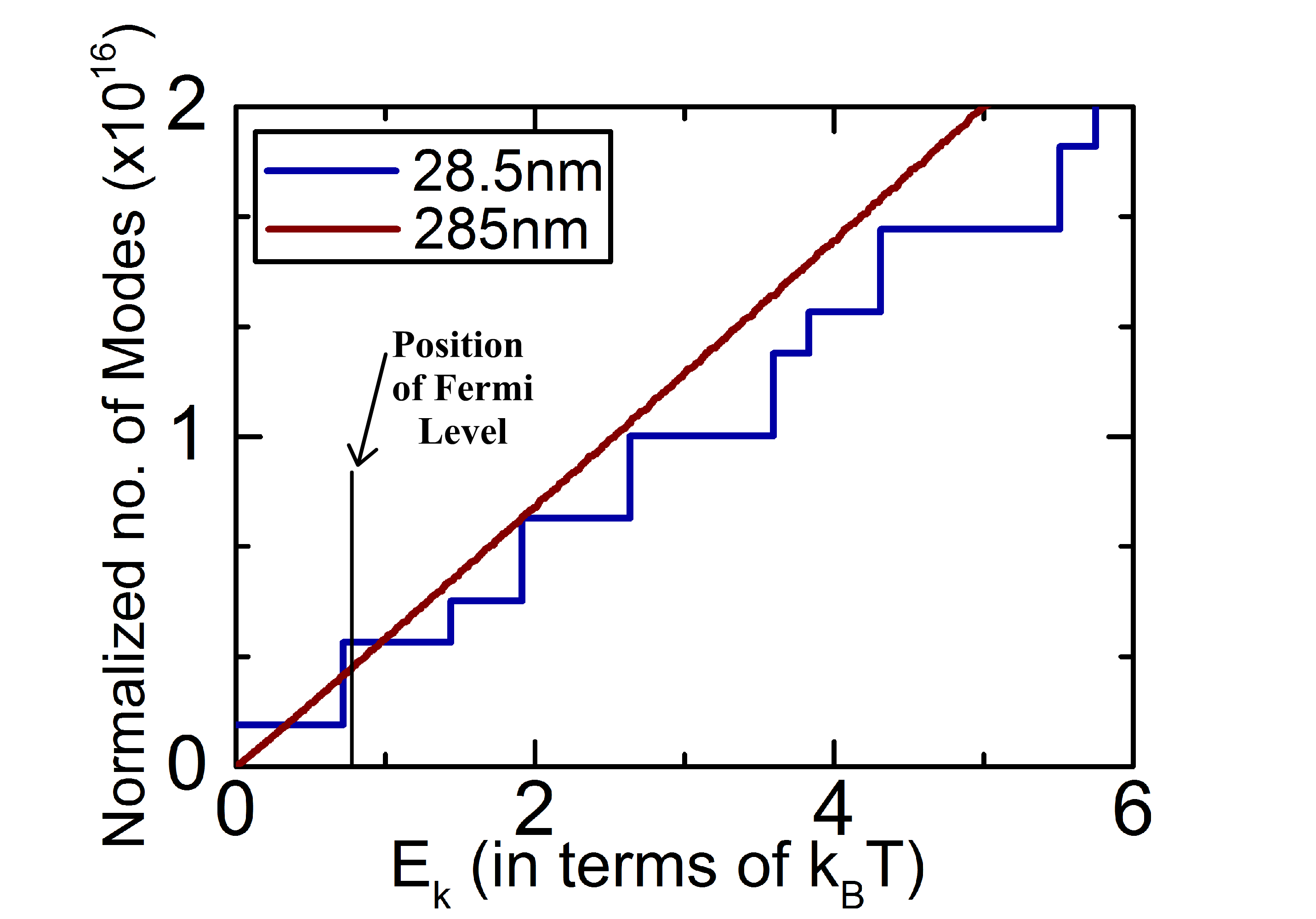
The reason for the degradation of power density in multi moded nanowires compared to bulk is evident from Fig. 5, which shows the normalized mode density per unit area of a 28.2nm and a 282nm wide square nanowire. Above the Fermi energy, the 282nm nanowire contains a higher number of modes per unit area which results in higher output power density. The degradation of the efficiency at maximum power is not so evident via a similar line of argument, since the efficiency is a ratio between the power and the heat current Muralidharan and Grifoni (2012); Agarwal and Muralidharan (2014). It is therefore of some use to make a back of the envelope calculation by considering for the two structures. In the linear response regime, the efficiency at maximum power is given by Benenti et al. (2014)
| (6) |
which is a monotonically increasing function of . The calculated value of for the and wide nanowires are and respectively, which proves that a nanowire of width would operate at higher compared to a nanowire of width . The calculations performed above are through circuit arguments Muralidharan and Grifoni (2012); Agarwal and Muralidharan (2014), which match the calculations performed by evaluating all the linear response coefficients in (1).
The domain of each regime in Figs. 4(a) and (b), however, would scale inversely as the effective mass () of the material and the temperature of operation . Thus, nanowires made of materials with higher effective mass would require smaller cross-section to harness the advantages of being single moded.
IV Operating Regimes of Nano-embedded Generators
We will now consider the effect of packing nanostructures and the details involved in the process of nano-embedding the structures considered so far. Embedded nanowires of cross-sectional dimensions and , with a separation between adjacent nanowires, provide a packing fraction of . Similarly embedded nanoflakes of width separated by energy barriers of width provide a packing fraction of . The details of the calculations are carried out in the appendix. It is of foremost importance to note that despite the higher power density provided by a single moded nanowire of cross-section , its effective power density in a matrix is limited due to a very low packing fraction.
A matrix packed with nanowires of square cross-section () separated by a energy barrier provides a packing fraction of 0.13. Similarly, nanoflakes packed in a matrix provide a packing fraction of 0.361, when adjacent flakes are separated by a energy barrier. These numbers are reduced to and respectively, if the separation between successive nanowires/flakes is increased to . We now turn our attention to the operating points of the respective thermoelectric generators taking their packing fraction into account. We use the term effective power density to denote the power per unit area of a matrix packed with nanowires/flakes.
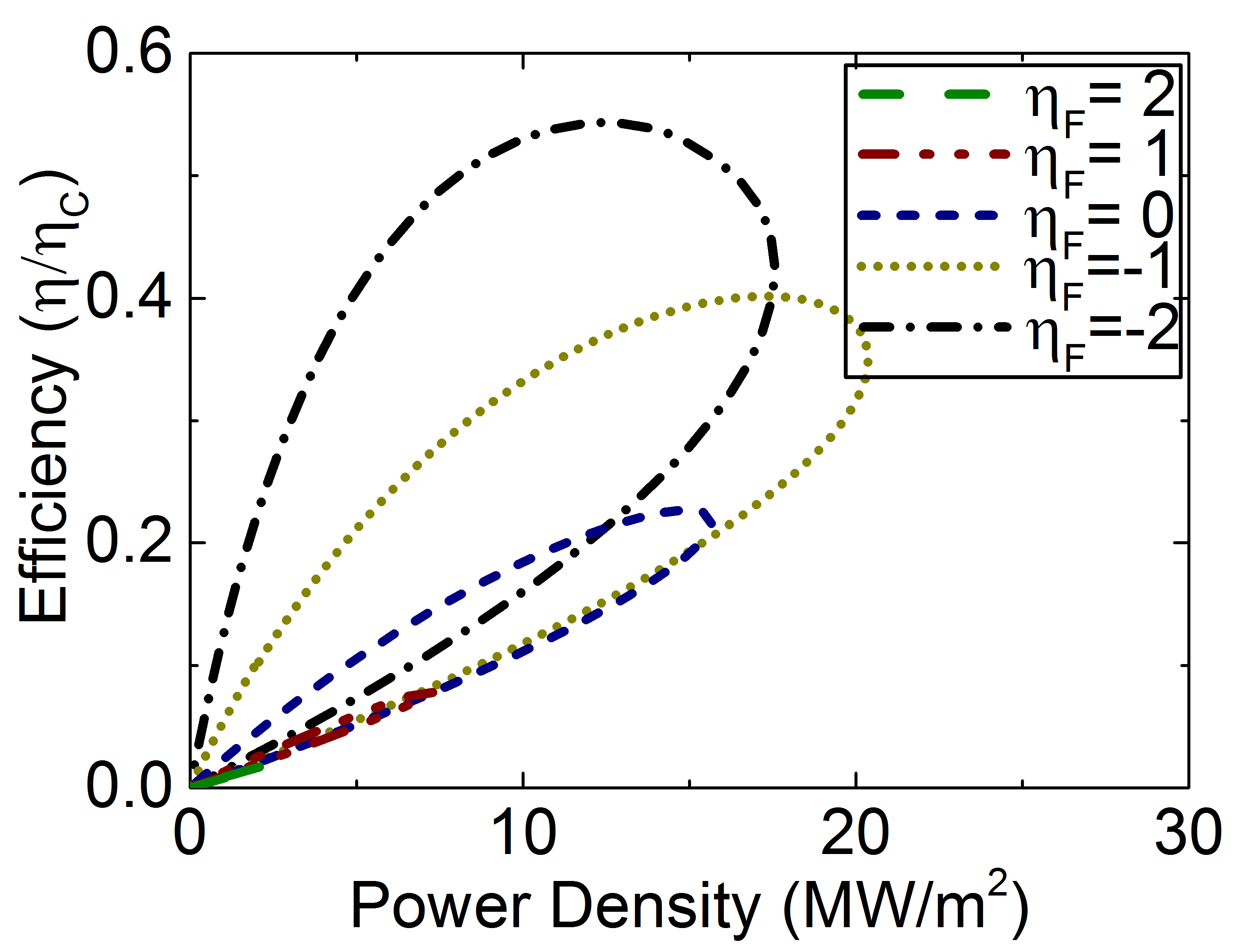
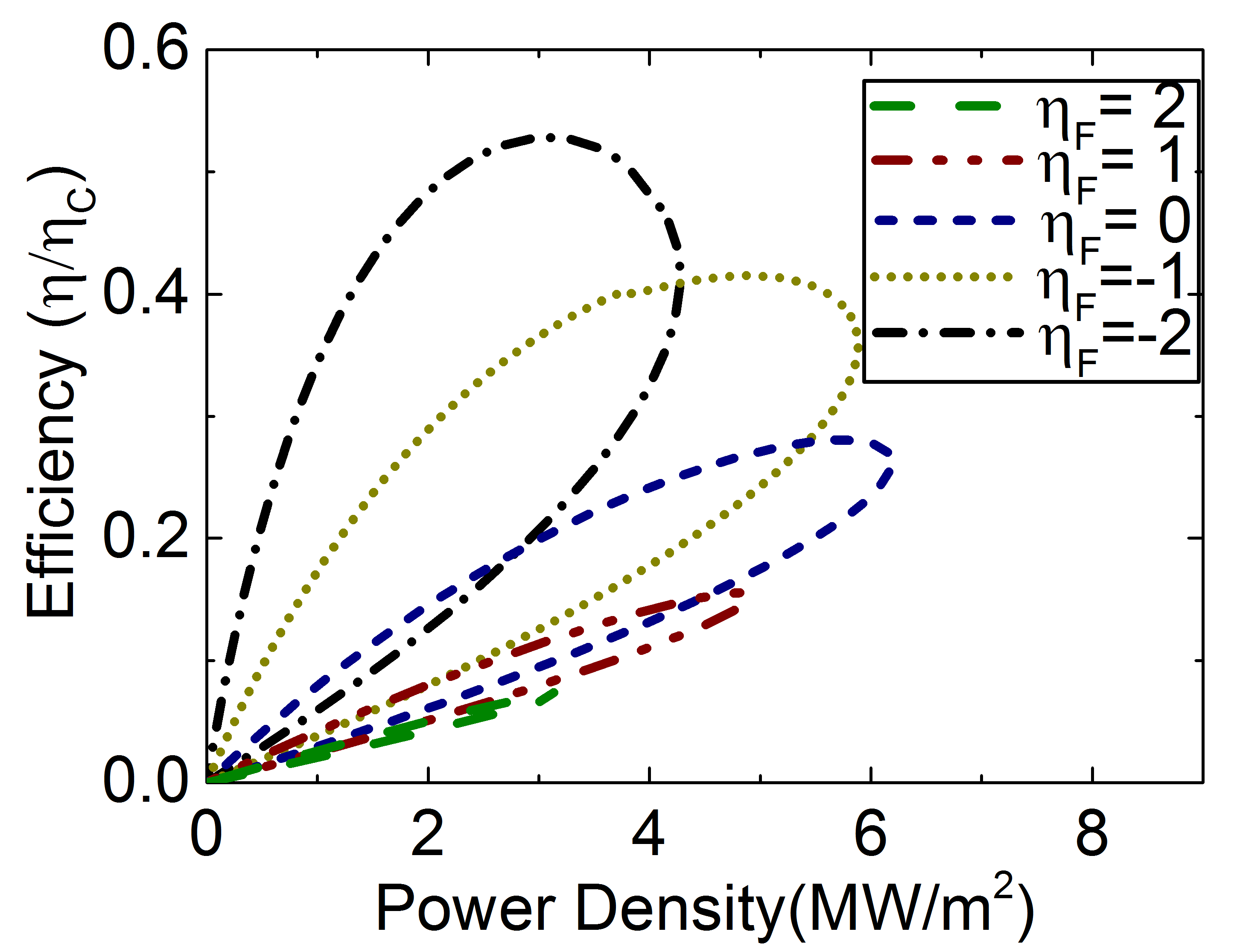
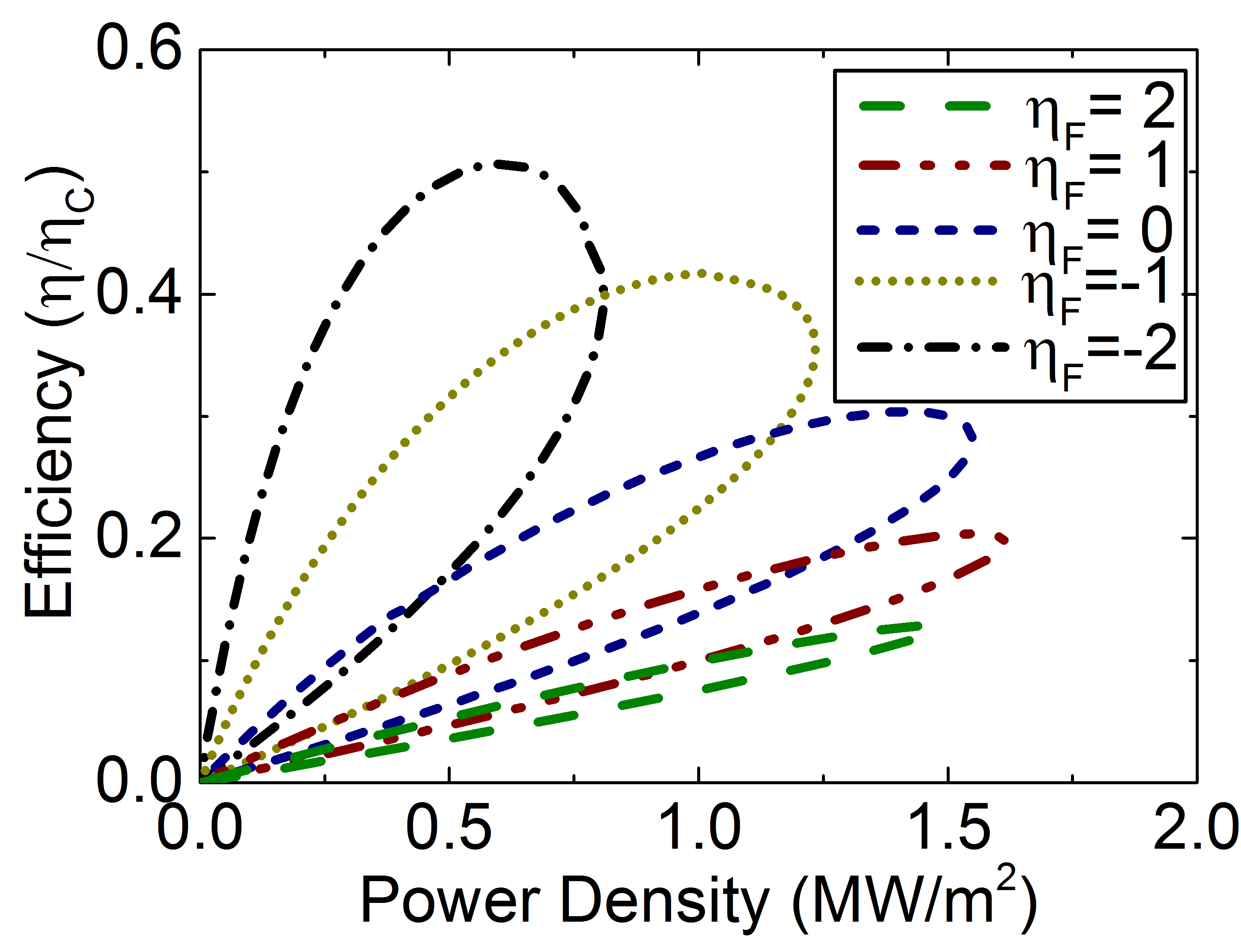
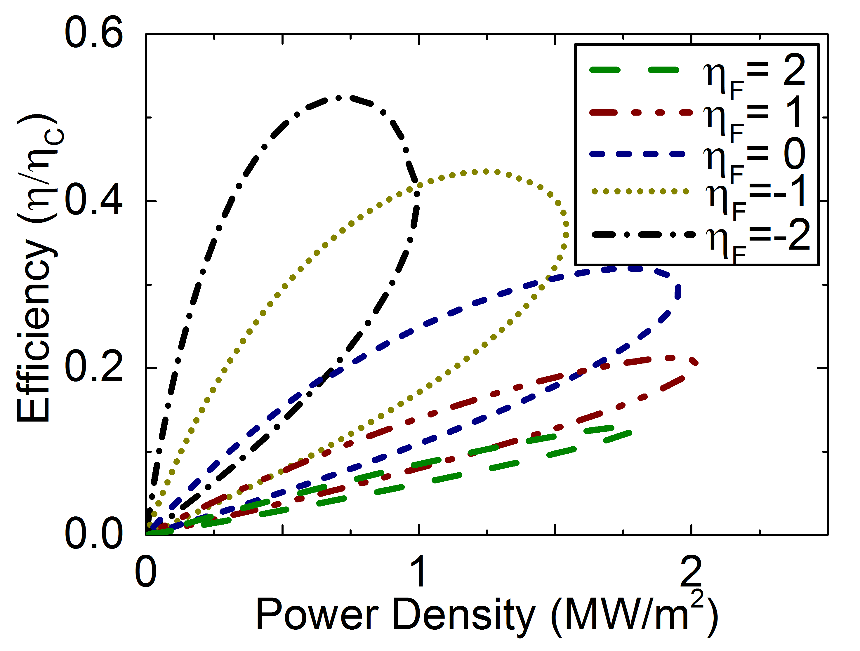
In the context of our discussion, operating points are defined as points in the effective power density-efficiency plane () where the effective power-density is maximum for a given efficiency or the efficiency is maximum for a given effective power-density. For power generation applications, these points offer the minimum effective power density-efficiency tradeoff. For bulk or nano-embedded generators, depending on the cross-sectional dimensions, material parameters and packing fractions, there is a set of points in the plane where the device can operate Whitney (2014), which we term as allowed points. The subset of all these points constitute the allowed region of operation in the plane. All other points in the plane constitute the forbidden region Whitney (2014). Operating points lie on the boundary of the allowed region and the forbidden region of operation. These are the points along which the maximum effective power density at a given efficiency, or equivalently, maximum efficiency at a given effective power density, can be obtained. Fig. 6 show the operating points of embedded nano-systems for a separation of and respectively. Each figure can be seen to be divided into three regimes:
Regime 1: In this regime, there is no trade-off between power and efficiency for the bulk thermoelectric generators, that is, efficiency increases monotonically with increasing power. Thermoelectric generators are not operated in this regime. This regime is marked using the light blue colour in Figs. 6(a) and (b).
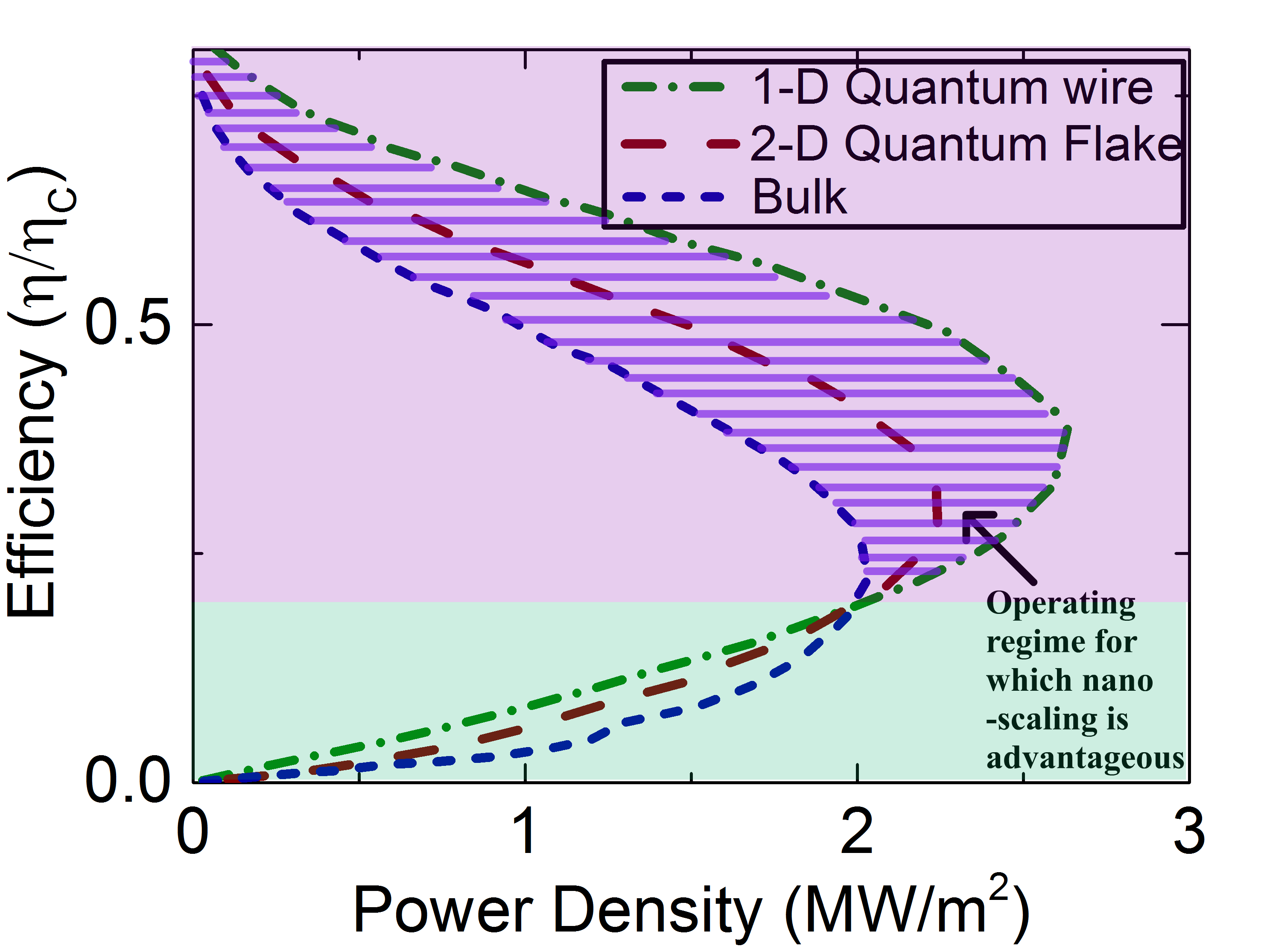
Regime 2: In this regime, there is a trade-off between power and efficiency for the bulk generators and bulk generators perform better in terms of the power density in comparison to nano-embedded systems. Using the bulk generator is advantageous in this regime. This regime is marked using the light yellow color in Figs. 6(a) and (b).
Regime 3: In this regime, there is a trade-off between power and efficiency for the bulk generator, but nano embedded systems perform better than the bulk in terms of power density at a given efficiency. In this region of operation, nano-embedding is advantageous. This regime is marked using the light purple color in Fig. 6(a) and (b).
It is shown in Fig. 6(a) that for nanowires/flake embedded systems of cross-sectional dimensions separated by energy barrier, the second regime does not exist. That is, for all relevant points of operation, nano-embedding is advantageous. However when the separation between adjacent nanowires/flakes is increased to , as noted in Fig. 6(b), nano-embedding is advantageous only in the regime of higher efficiency. This could be understood by the fact that increasing separation between adjacent nanowires/flakes decreases the packing density resulting in a decrease in the effective power output per unit area.
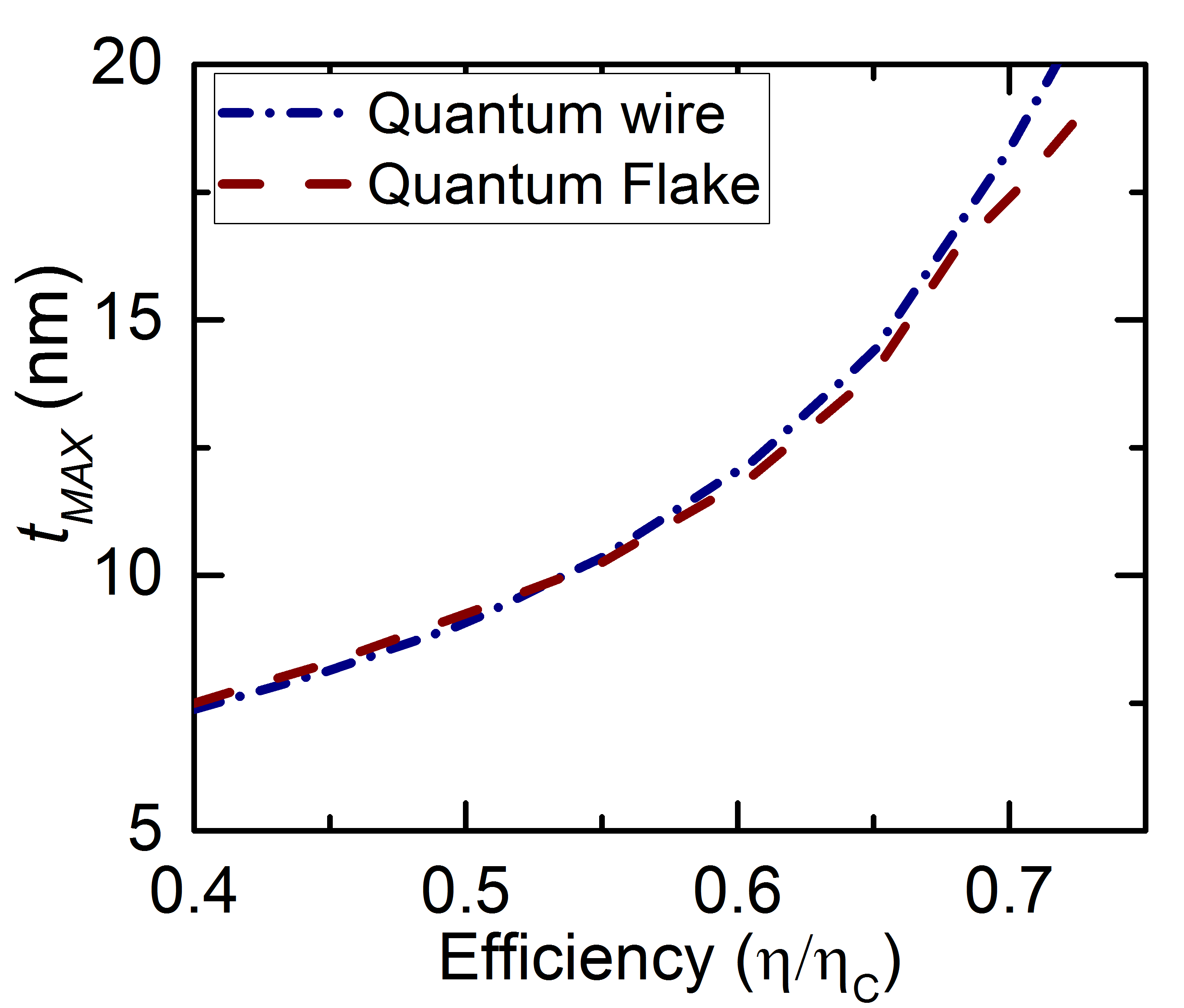
In this context, it may be of particular interest to know what is the maximum width by which two nano devices may be separated while still retaining the power-efficiency advantage out of nano-embedding. This is shown in Fig. 7, where the maximum possible separation between two nano-scale devices increases when the device is operated at a higher efficiency. In other words, for the same separation between two nano-generators, nano-scaling offers a higher power advantage when they are operated in higher efficiency regime.
V Advantage Factor due to Nano-Scaling
A metric to quantify the power advantage offered by nano-embedded systems over their bulk counterpart serves as a deciding factor for nano-scaling thermoelectric generators. The parameter of interest, is indeed, the factor by which the power density is increased in nano embedded systems over bulk generators.
In the context of our discussion, we define an advantage factor at a given efficiency as
where is the effective power density of a nano-embedded thermoelectric generator and is the power density of the bulk thermoelectric generator. The advantage factor is a basic measure of the advantage we get from nano-embedding. For a given set of material parameters, the advantage factor depends on (a) the efficiency of operation of the thermoelectric generators and (b) the effective area per nano-generator. We define effective area of a nano-generator as
where is the number of nano generators embedded in a square matrix of unit cross-sectional area. Fig. 8(b) shows the logarithm of the advantage factor versus the efficiency for nano-embedded GaAs generators of cross-sectional dimension separated by a AlAs energy barrier. Doubling the effective area per unit nano-scale generator decreases at each point on Fig. 8 by approximately 0.3dB. For square embedded nanowires of cross-sectional dimensions w separated by energy barriers of width t, the effective area is given by .
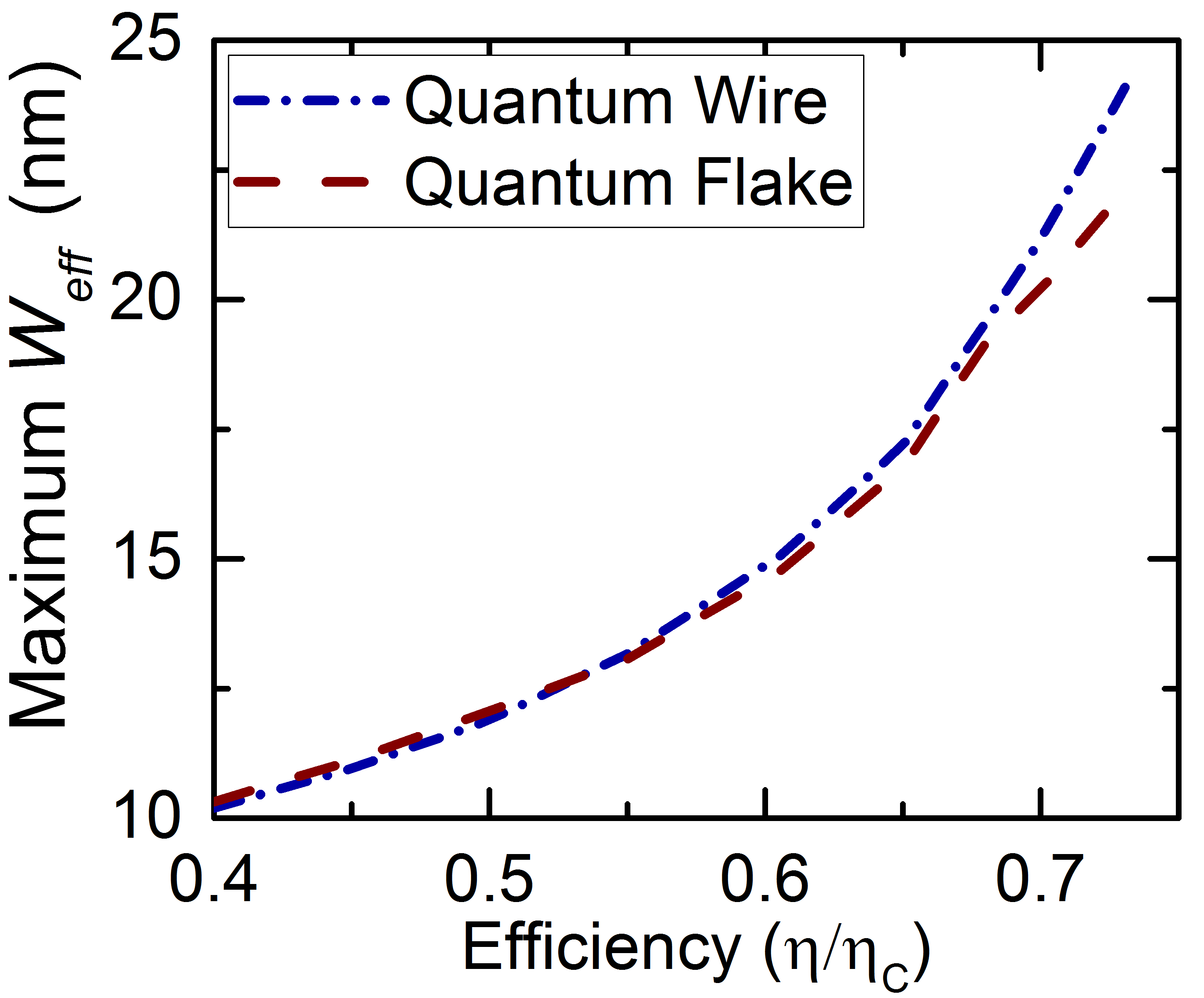
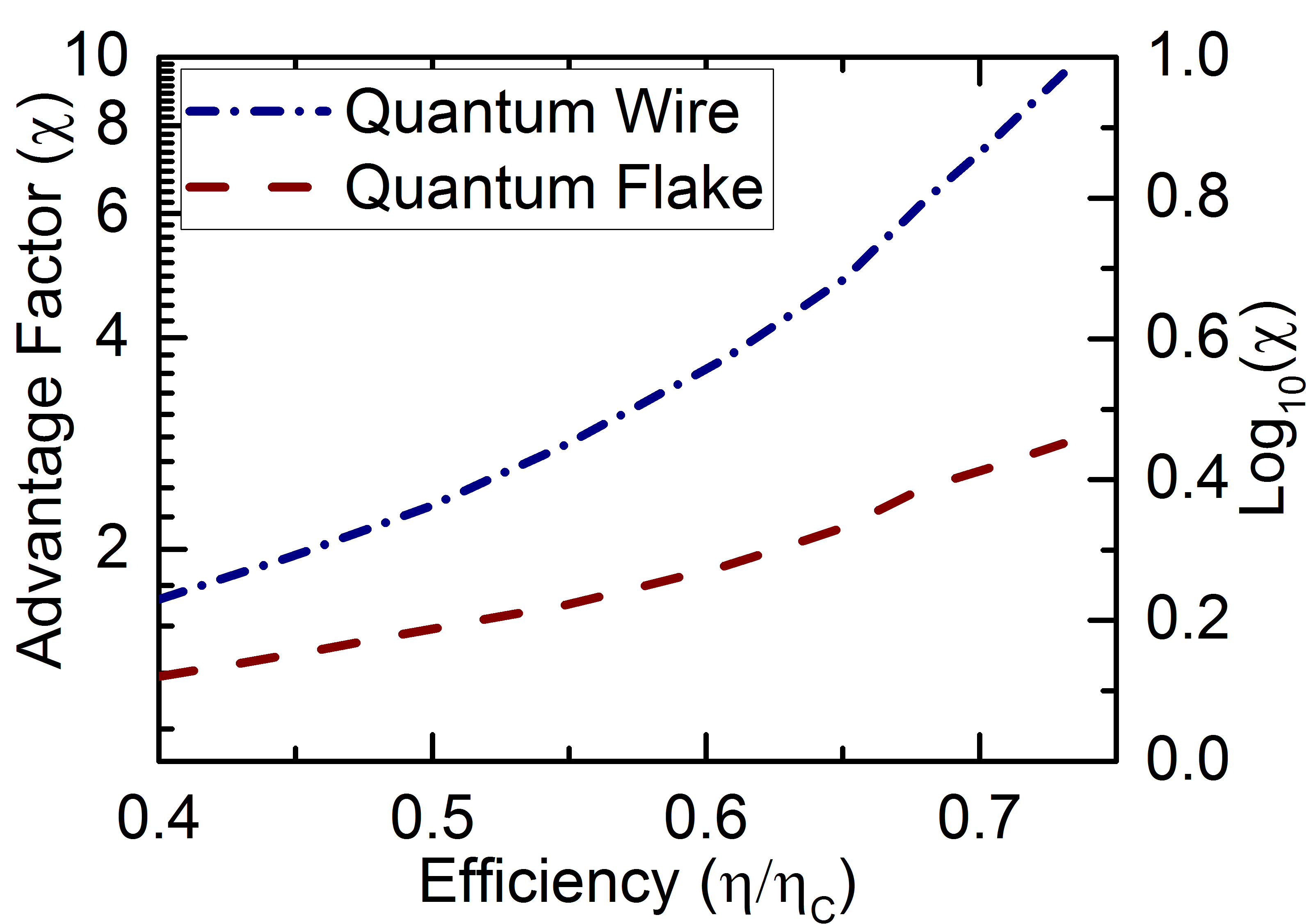
For embedded nanoflakes of width w and separated by energy barriers of width t, the effective area is given by . The quantity is therefore a parameter of importance and we call it the effective width () of the nano-embedded generators. A lower results in a higher advantage factor. Fig. 8(a) shows the maximum effective width that can be allocated to a unit nano embedded generator with the effective width maximum when . In terms of the maximum effective width, the advantage factor may be written as: , for a single moded nanowire and for a nanoflake with a single mode along confined direction. For the same effective width, nanowires perform better than nanoflakes, the difference in their advantage factors being an increasing function of the efficiency. It should be noted that advantage factor is calculated along the operating points at a given efficiency for single moded nanowires and flakes.
VI Conclusion
In this work, we have pointed out a few crucial aspects to be considered for the electronic engineering of nano-embedded bulk thermoelectric generators. First and foremost, we pointed out that a performance degradation is inevitable as the nanostructure transitions to being multi moded, a trend which has been noted in a few experiments Hochbaum et al. (2008b); Boukai et al. (2008b). Turning to packing strategies, we pointed out that at higher packing fractions, nano-embedding offers a significant power density advantage when operated over a large range of efficiencies. However, at lower packing fractions, nano-embedding performs poorly, displaying only a marginal advantage and that too, only when operated at much higher efficiencies. Finally, we introduced a metric - the advantage factor, to elucidate quantitatively, the enhancement in the power density offered via nano-embedding at a given efficiency. At the end, we explored the maximum effective width of nano-embedding which serves as a reference in designing nano-embedded generators in the efficiency range of interest. From our detailed analysis, we conclude that although a nanowire/flake is capable of demonstrating enhanced nano-scale thermoelectric properties Hicks and Dresselhaus (1993a, b) upto a maximum cross-sectional dimensions of , it is advantageous to fix the width of nanowires/flakes to the smallest possible value permitted by current fabrication capabilities. In all our calculations, we have neglected decrease in efficiency due to lattice heat conductivity. Although the performance of both nano-embedded generators and traditional generators are degraded due to heat conduction via phonons, nano-structuring offers a predominant advantage over traditional generators in terms of reduced lattice conductivity. The high density of interfaces in nano embedded generators on the length scale of phonon mean free path effectively scatters long wavelength phonons thereby reducing the lattice conductivity Mingo and Broido (2004); Mingo (2004); Zhou et al. (2007, 2010); Boukai et al. (2008a); Hochbaum et al. (2008a); Poudel et al. (2008); Balandin et al. (1999) and counteracting the reduction in efficiency to a large extent. Analysis and results obtained in this work should provide general design guidelines to embed nanostructures within a bulk matrix to offer a greater advantage over traditional bulk thermoelectrics, within the limits of current fabrication technologies.
Appendix
VI.1 Evaluation of Packing Fraction
Let us assume rectangular nano-structures embedded in a bulk matrix. Let the height and width of each nano-scale device be and respectively. Assuming the cross-sectional dimensions of the bulk material (say and ) to be much greater than the cross-sectional dimensions of the nano-structures and the minimum separation width between two nano-scale structures to be the total number of nano structures that can be embedded in the bulk matrix is
In the context of our discussion, the packing fraction is defined as the fraction of the 3-D matrix which is occupied by the embedded nano structures. From this definition, the packing fraction for embedded nano structures in the matrix is
For square 1-D nano-scale structures, . The packing fraction then becomes
For 2-D nano-scale structures, we have . So, the packing fraction is given by
VI.2 Calculation of maximum effective width ()
Let us assume the power density of bulk thermoelectric generator is at an efficiency . At the same efficiency, let power output of a unit embedded nanowire be . We calculate the effective width of unit nano generator when the overall power density of the bulk is equal to the overall power density of the embedded nano generators. The number of single moded nanowires required to match the power density of the bulk is:
We need to pack a minimum min number of single moded nanowires per unit area of the matrix to achieve the power density similar to a bulk generator. To gain the advantage embedded nanowires, nanowires must be packed per unit area of the matrix such that
Assuming the nanowires to be of square cross-section, the maximum effective area which can be allocated for a unit nano generator is :
So, the maximum effective width of unit nano generator should be
Similar derivations for 2-D nano-scale devices lead to:
where is the power output of a 2-D quantum flake which has only one conducting mode along the confined dimension.
References
- Hicks and Dresselhaus (1993a) L. D. Hicks and M. S. Dresselhaus, Phys. Rev. B 47, 12727 (1993a).
- Hicks and Dresselhaus (1993b) L. D. Hicks and M. S. Dresselhaus, Phys. Rev. B 47, 16631 (1993b).
- Snider and Toberer (2008) G. J. Snider and E. S. Toberer, Nature Mater. 7, 105 (2008).
- Dresselhaus et al. (2007) M. Dresselhaus, G. Chen, M. Tang, R. Yang, H. Lee, D. Wang, Z. Ren, J.-P. Fleurial, and P. Gogna, Advanced Materials 19, 1043 (2007).
- Heremans et al. (2008) J. P. Heremans, V. Jovovic, E. S. Toberer, A. Saramat, K. Kurosaki, A. Charoenphakdee, S. Yamanaka, and G. J. Snyder, Science 321, 554 (2008).
- Muralidharan and Grifoni (2012) B. Muralidharan and M. Grifoni, Phys. Rev. B 85, 155423 (2012).
- Nakpathomkun et al. (2010) N. Nakpathomkun, H. Q. Xu, and H. Linke, Phys. Rev. B 82, 235428 (2010).
- Sothmann et al. (2013) B. Sothmann, R. Sanchez, A. Jordan, and M. Buttiker, New J. Phys. 15, 095021 (2013).
- Agarwal and Muralidharan (2014) A. Agarwal and B. Muralidharan, Applied Physics Letters 105, 013104 (2014).
- Mingo and Broido (2004) N. Mingo and D. A. Broido, Phys. Rev. Lett. 93, 246106 (2004).
- Mingo (2004) N. Mingo, Applied Physics Letters 84, 2652 (2004).
- Zhou et al. (2007) F. Zhou, J. Szczech, M. T. Pettes, A. L. Moore, S. Jin, and L. Shi, Nano Letters 7, 1649 (2007), pMID: 17508772.
- Zhou et al. (2010) F. Zhou, A. L. Moore, M. T. Pettes, Y. Lee, J. H. Seol, Q. L. Ye, L. Rabenberg, and L. Shi, Journal of Physics D: Applied Physics 43, 025406 (2010).
- Boukai et al. (2008a) A. I. Boukai, Y. Bunimovich, J. Tahir-Kheli, J.-K. Yu, W. A. Goddard, and J. R. Heath, Nature 451, 168 (2008a).
- Hochbaum et al. (2008a) A. I. Hochbaum, R. Chen, R. D. Delgado, W. Liang, E. C. Garnett, M. Najarian, A. Majumdar, and P. Yang, Nature Publishing Group 451, 163 (2008a).
- Poudel et al. (2008) B. Poudel, Q. Hao, Y. Ma, Y. Lan, A. Minnich, B. Yu, X. Yan, D. Wang, A. Muto, D. Vashaee, X. Chen, J. Liu, M. S. Dresselhaus, G. Chen, and Z. Ren, Science 320, 634 (2008).
- Goldsmid (2009) Goldsmid, Introduction to Thermoelectricity (Springer, 2009).
- DiSalvo (1999) F. J. DiSalvo, Science 285, 703 (1999).
- Shakouri (2011) A. Shakouri, Annual Review of Materials Research 41, 399 (2011).
- Giazotto et al. (2006) F. Giazotto, T. T. Heikkilä, A. Luukanen, A. M. Savin, and J. P. Pekola, Rev. Mod. Phys. 78, 217 (2006).
- Muhonen et al. (2012) J. T. Muhonen, M. Meschke, and J. P. Pekola, Reports on Progress in Physics 75, 046501 (2012).
- Paulsson and Datta (2003) M. Paulsson and S. Datta, Phys. Rev. B 67, 241403 (2003).
- Reddy et al. (2007) P. Reddy, S.-Y. Jang, R. A. Segalman, and A. Majumdar, Science 315, 1568 (2007).
- Kim et al. (2009) R. Kim, S. Datta, and M. S. Lundstrom, Journal of Applied Physics 105, 034506 (2009).
- Yang et al. (2005) R. Yang, G. Chen, and M. S. Dresselhaus, Phys. Rev. B 72, 125418 (2005).
- Fuechsle et al. (2012) M. Fuechsle, J. A. Miwa, S. Mahapatra, H. Ryu, S. Lee, S. Lee, O. Warschkow, L. C. L. Hollenberg, and G. Klimeck, Nature Nanotechnology 7, 242 (2012).
- Cen et al. (2009) C. Cen, S. Thiel, J. Mannhart, and J. Levy, Science 323, 1026 (2009).
- Whitney (2014) R. S. Whitney, Physical Review Letters 112, 130601 (2014).
- Mahan and Sofo (1996) G. D. Mahan and J. O. Sofo, Proc. Natl. Acad. Sci. U.S.A. 93, 7436 (1996).
- Humphrey and Linke (2005) T. E. Humphrey and H. Linke, Phys. Rev. Lett. 94, 096601 (2005).
- Esposito et al. (2009a) M. Esposito, K. Lindenberg, and C. Van den Broeck, Phys. Rev. Lett. 102, 130602 (2009a).
- Esposito et al. (2009b) M. Esposito, K. Lindenberg, and C. V. den Broeck, EPL (Europhysics Letters) 85, 60010 (2009b).
- Esposito et al. (2010) M. Esposito, R. Kawai, K. Lindenberg, and C. Van den Broeck, Phys. Rev. Lett. 105, 150603 (2010).
- Streetman (1995) B. G. Streetman, Solid State Electronic Devices (4th Ed.) (Prentice-Hall, Inc., 1995).
- Ribeiro, M. et al. (2011) Ribeiro, M., Fonseca, L. R. C., and Ferreira, L. G., EPL 94, 27001 (2011).
- Wang et al. (2013) Y. Wang, F. Zahid, Y. Zhu, L. Liu, J. Wang, and H. Guo, Applied Physics Letters 102, 132109 (2013).
- Datta (2005) S. Datta, Quantum Transport: Atom to Transistor (Cambridge University Press, 2005).
- Benenti et al. (2014) G. Benenti, G. Casati, and C. Mejía-Monasterio, New Journal of Physics 16, 015014 (2014).
- Hochbaum et al. (2008b) A. I. Hochbaum, R. Chen, R. D. Delgado, W. Liang, E. C. Garnett, M. Najarian, A. Majumdar, and P. Yang, Nature Publishing Group 451, 163 (2008b).
- Boukai et al. (2008b) A. Boukai, Y. Bunimovich, J. T. Kheli, J. K. Yu, W. A. Goddard III, and J. R. Heath, Nature Publishing Group 451, 168 (2008b).
- Balandin et al. (1999) A. Balandin, A. Khitun, J. Liu, K. Wang, T. Borca-Tasciuc, and G. Chen, in Eighteenth International Conference on Thermoelectrics (1999) pp. 189–192.