Local Spectroscopic Characterization of Spin and Layer Polarization in WSe2
Abstract
We report scanning tunneling microscopy (STM) and spectroscopy (STS) measurements of monolayer and bilayer WSe2. We measure a band gap of 2.21 0.08 eV in monolayer WSe2, which is much larger than the energy of the photoluminescence peak indicating a large excitonic binding energy. We additionally observe significant electronic scattering arising from atomic-scale defects. Using Fourier transform STS (FT-STS), we map the energy versus momentum dispersion relations for monolayer and bilayer WSe2. Further, by tracking allowed and forbidden scattering channels as a function of energy we infer the spin texture of both the conduction and valence bands. We observe a large spin-splitting of the valence band due to strong spin-orbit coupling, and additionally observe spin-valley-layer coupling in the conduction band of bilayer WSe2.
pacs:
68.37.Ef,73.20.At,73.22.-f,75.70.TjTransition metal dichalcogenides (TMDs) have gained great popularity recently for their potential applications in optical and electronic devices Xu et al. (2014). The band gaps of these materials lie in the visible part of the spectrum, and undergo an indirect-to-direct transition at monolayer thickness. In monolayers, the band extrema (valleys) lie at the K and K’ points com , and the lack of inversion symmetry leaves these valleys physically distinguishable (for example, via optical selection rules). The heavy transition metals in TMDs also contribute to strong spin-orbit coupling (SOC) for band edge carriers, with especially large effects expected for the tungsten dichalcogenides such as WSe2. This SOC leads to an out-of-plane Zeeman-type spin splitting of the valence band as large as 500 meV, with opposite spin polarizations at the K and K’ valleys due to time reversal symmetry leading to a coupling of the spin and valley degrees of freedom.
AB-stacked bilayer TMDs are inversion symmetric, and as a consequence the spin and valley polarizations of the top layer are opposite those of the bottom, thus effectively restoring spin and valley degeneracy. They additionally exhibit an extra degree of freedom characterized by a layer pseudospin. In WSe2, the SOC is larger than the interlayer hopping amplitude, thus localizing the carriers by layer near the Brillouin zone (BZ) corners and leading to a coupling of the spin, valley, and layer degrees of freedom (see Ref. Xu et al., 2014 for a review of these properties). Numerous spintronic and valleytronic applications have been proposed to exploit these degrees of freedom in TMD monolayers and bilayers Xiao et al. (2012); Cao et al. (2012); Mak et al. (2012); Lu et al. (2013); Wu et al. (2013); Gong et al. (2013); Yuan et al. (2013); Jones et al. (2013, 2014); Xu et al. (2014); Mak et al. (2014); Yuan et al. (2014).

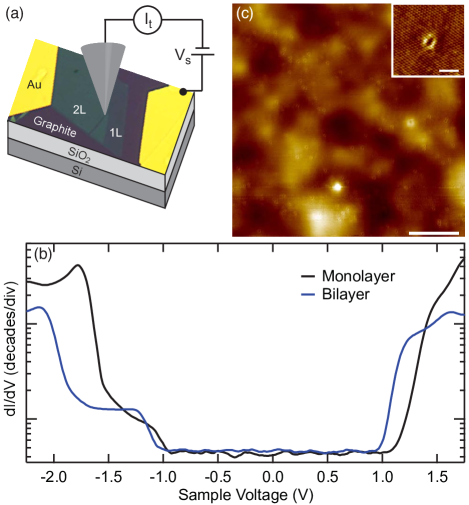
Significant work has been performed to characterize these polarizations in WSe2 with direct optical excitation Jones et al. (2013, 2014); Aivazian et al. (2015); Srivastava et al. (2015) and spin-resolved ARPES Riley et al. (2014); Le et al. (2015). However, the former is unable to capture physics away from direct transitions (i.e. away from the BZ corners) and the latter cannot probe unoccupied (conduction band) states. Here we directly probe the electronic states of monolayer and bilayer WSe2 via STM and STS measurements in order to gain a deeper understanding of its band structure and internal quantum degrees of freedom. Fig. 1(a) shows a schematic of our measurement setup. All measurements were performed in ultrahigh vacuum at a temperature of 4.5 K. WSe2 sits on a graphite flake to provide a conducting substrate for collecting the tunnel current. The sample was fabricated using a dry-peel transfer technique Wang et al. (2013); Zomer et al. (2014). WSe2 and graphite were mechanically exfoliated onto separate SiO2 substrates, then the WSe2 flake was picked up using a polycarbonate film and micro-mechanically aligned onto a graphite flake. Cr/Au electrodes were written using electron beam lithography, and the sample was annealed overnight in vacuum at 300 ∘C.
Fig. 1(b) shows representative dI/dV spectroscopy for monolayer and bilayer WSe2. We extract the electronic band gap of both by measuring the energy range where the dI/dV spectroscopy is zero, from which we find Eg = 2.21 0.08 eV for monolayer and 2.14 0.05 eV for bilayer WSe2. This is significantly larger than the typically observed optical gaps in monolayer and bilayer WSe2 (1.65 eV and 1.6 eV, respectively) Zhao et al. (2013); Zeng et al. (2013); Zhang et al. (2014), indicative of a giant excitonic binding energy Ugeda et al. (2014). We note that this spectroscopically extracted gap actually represents the separation of the onset of tunneling into the valence and conduction band extrema, which, due to the finite width of the bands, is smaller than the separation between the center of the valence band maximum and the conduction band minimum. The peaks and/or inflection points in the dI/dV spectrum likely represent the band centers, which would imply a band gap a few hundred meV larger than that extracted above, in reasonably good agreement with the GW level DFT calculated gap Ding et al. (2011); Ramasubramaniam (2012). Due to small changes in the tip work function resulting from the tip shaping procedure (for example, pulsing a gold particle onto the end of the tip), we have occasionally observed small (150 meV) rigid shifts of the entire dI/dV spectrum in sample voltage. To account for this, we take dI/dV spectroscopy before all measurements, and when necessary offset the sample voltage to match the dI/dV reference spectra of Fig. 1(b).
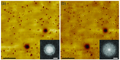
Topographic maps of WSe2 exhibit a significant density of defects. Fig. 1(c) shows one such example for bilayer WSe2, in which two species of defects are present. There are small atomic-scale defects throughout the image (the inset is an atomically-resolved image of one such defect), along with two larger scale defects. These defects are more clearly visible in spatially resolved dI/dV maps, as shown in Figs. 2(a) and (b) for the same area as in Fig. 1(c), taken at sample voltages of Vs = -1.35 V and -1.5 V, respectively. In bilayer WSe2, defects of a given species appear with two clearly distinct strengths, where the weaker defects presumably reside in the lower WSe2 layer. This indicates we are capable of probing electrons in both layers. In monolayer WSe2, all defects are observed with similar strength as they all reside in the same layer SM . By counting the number of defects in numerous dI/dV maps taken on monolayer WSe2, we find a defect density of 1.1 0.3 x 1012 cm-2 for the smaller defects, and approximately two orders of magnitude lower density for the large defects. Given the similar appearance of sulfur vacancies observed in MoS2 Lu et al. (2014) it is likely that the small defects we observe here are due to selenium vacancies, although a full defect characterization is outside the scope of this work.

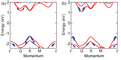
These defects act as scattering centers for the electrons in WSe2, resulting in Friedel oscillations visible as concentric rings surrounding each defect Friedel (1952). The wavelength of these oscillations at a given energy is controlled by the band structure of the WSe2. So, for example, since the valence band grows wider as the energy is lowered (Fig. 2(a) to (b)), the wavelength of the oscillations grows shorter as they are inversely proportional. FT-STS provides direct visualization of the available scattering channels for electrons in momentum space Hoffman et al. (2002). The long-wavelength Friedel oscillations of Figs. 2(a) and (b) are due to intravalley scattering processes and show up as disk-like features at the center of their respective Fourier transforms (insets). The signal in the Fourier transform can be understood as a map of the joint density of states (JDOS) of the band structure. The intravalley scattering process with the largest possible momentum transfer connects one side of a given valley to the other, setting the radius of the disk observed in the Fourier transform. The disk is then filled in by all other smaller momentum transfer scattering processes connected within a single valley. As a result, the radius of the central scattering disk gives a measure of the size of the Fermi surface at a given sample voltage. The blue dots in Figs. 3(a) and (b) mark the momentum extracted from the size of these scattering disks as a function of sample voltage, providing experimental maps of the band structures of monolayer and bilayer WSe2 (see the Supplemental Material SM for details on wave vector extraction and band assignments). Data from different sets of dI/dV maps taken with different tips and at different spots on the sample are all plotted together, as they follow the same general trend. Data points have been plotted on both sides of a given valley since the Fermi surfaces are roughly circular.

We confirm our extracted energy versus momentum dispersion by comparing with the calculated ab initio band structures of monolayer and bilayer WSe2 with spin-orbit coupling terms included (solid red lines in Fig. 3), taken directly from Ref. Zeng et al., 2013. Since the size of the band gap is not well constrained in these calculations, it has been manually set to match the band edges extracted from the dI/dV spectroscopy in Fig. 1(b) (plus a small offset to account for the finite band width). Our experimental results are in reasonable agreement with the theoretically anticipated bands; most notably the effective masses generally match well with the theoretically predicted values. The extracted bands at near -2 eV are around a hundred meV below the calculated bands for both monolayer and bilayer WSe2, suggesting possible discrepancies between the DFT calculation and the true band structure. Disagreements may also result from mixing of the scattering signals of two bands.

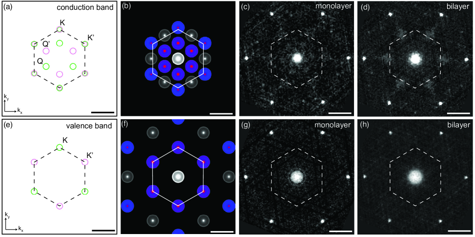
In addition to the intravalley scattering channels, there could, in principle, be scattering between different valleys. Such scattering occurs with larger momentum transfer than intravalley scattering, and therefore the resonances should be further from the center of the Fourier transforms. Due to strong spin-orbit coupling in WSe2, the valence band at the K point, which is primarily comprised of =2 -orbitals of W Roldán et al. (2014a, b), is spin-split by around 450 meV, with bands having opposite spins in the K and K’ valleys. Fig. 4(e) shows a schematic of the band structure of monolayer WSe2 at an energy between the two spin-split valence bands. There are six Fermi pockets surrounding the K and K’ valleys, alternating between spin up at K (green) and spin down at K’ (pink). Without this spin texture, atomic-scale defects would induce intervalley scattering, identified by resonances in the Fourier transform at , where is the WSe2 lattice constant ( times closer to the center than the lattice resonances, and rotated from them by 30∘). However, the spin polarization of the valleys is expected to suppress these resonances, as the intervalley scattering process now additionally requires a spin-flip which non-magnetic defects are unable to provide.
We simulate the Fourier transform anticipated for each case by calculating the both the spin-dependent and -independent JDOS of the band structure shown in Fig. 4(e) Roushan et al. (2009). The result is plotted in Fig. 4(f), where the colored features correspond to scattering resonances expected only in the case of bands lacking spin polarization. The central resonance represents the intravalley scattering discussed previously, and its diameter is twice the diameter of the K-point bands. Due to the geometry of the chords which can connect two points on the constant energy contour, the scattering signal decays away from the center of the Fourier transform but becomes large again just around the circumference of the disk, which is in good agreement with the features we observe in the maps shown in the insets of Fig. 2. Fig. 4(g) shows a comparable symmetrized Fourier transform of an atomically resolved dI/dV map taken on monolayer WSe2 SM . The features anticipated from K-valley mixing are conspicuously absent despite the high density of atomic-scale defects normally capable of inducing such scattering, implying the anticipated spin-polarization of the valleys. In contrast, this valley mixing is readily observable in graphene with atomic-scale defects Rutter et al. (2007), which lacks the spin polarization of the K-point valleys Castro Neto et al. (2009).
In the conduction band, the lowest energy bands exist around the K and Q points, the latter of which is not a high symmetry point but occurs about halfway between and K. Fig. 4(a) shows a general schematic of the Fermi surface in the conduction band along with the spin polarization theoretically anticipated for WSe2 Kormányos et al. (2015). While there is only a small spin-splitting anticipated at the K point (50 meV) since these bands are predominately =0 -orbitals of W Kośmider et al. (2013), the Q-point bands are expected to be split by over 200 meV in monolayer and 500 meV in bilayer WSe2 since they are comprised of both =1 -orbitals of Se and =2 -orbitals of W Roldán et al. (2014a, b). Fig. 4(b) shows the JDOS calculation for the conduction band with the same color coding scheme as in Fig. 4(f). The K-point bands are removed from the calculation to reflect the fact that they are not expected to factor significantly into the observed scattering processes due to the reduced tunnel probability into K in the monolayer SM , and do not exist for the bottom-most 250 meV of the bilayer conduction band. Fig. 4(c) shows the Fourier transform at the bottom of the conduction band of monolayer WSe2. Similar to the case of the valence band, only the features allowed assuming spin-polarized bands are present (note that the features corresponding to Q to Q scattering along the sides of the hexagonal Brillouin zone are present but very weak.)
The spin degeneracy of the spin-split bands is restored in bilayer WSe2 due to the inversion symmetry of the layers. So, for example, if a given band in the bottom layer is spin down, that same band in the upper layer will be spin up. Despite the restored spin degeneracy, the Fourier transforms of our experimental dI/dV maps in the bilayer conduction band (Fig. 4(d)) and the valence band (Fig. 4(h)) do not exhibit all the resonances anticipated in the simulation tun . They do, however, match the exact subset of resonances expected given spin-polarized bands (white features in Figs. 4(b) and (e)). Put another way, the bilayer maps exhibit only the features observed in the monolayer maps, implying an effective spin-polarization of the bilayer WSe2 bands. This spin-polarization arises from strong layer-polarization of the bilayer WSe2. Since there is only a small component of in the Q- and K-point bands, the spin-orbit coupling dominates over the interlayer hopping, thus enhancing the layer polarization. As we are capable of probing electrons in both layers of bilayer WSe2, the observation of nearly identical Fourier transforms for monolayer and bilayer WSe2 provides direct evidence of strong spin-layer-valley entanglement in both the valence and conduction bands.
We have presented local tunnel spectroscopy measurements of monolayer and bilayer WSe2. By examining electronic scattering from atomic-scale defects we are able to map out portions of the band structure of the material, as well as to identify scattering pathways forbidden by spin and layer polarizations of the bands. Our results directly demonstrate that intervalley electronic scattering is suppressed in the valence band of monolayer WSe2 as a result of the large spin-splitting of those bands. Furthermore, we observe strong layer-polarization in bilayer WSe2, providing the first experimental evidence of the spin-valley-layer coupling in the conduction band. While previous applications have been proposed to utilize this effect for slightly hole-doped bilayer WSe2 Gong et al. (2013), our results present a path towards realizing these novel combined spintronic and valleytronic applications in devices of either doping.
Acknowledgements.
The authors thank Gui-Bin Liu and Wang Yao for supplying the calculated band structures and for valuable discussions. The authors also thank Allan H. MacDonald for valuable theoretical discussions. The work at Arizona was partially supported by the U. S. Army Research Laboratory and the U. S. Army Research Office under contract/grant number W911NF-14-1-0653 and the National Science Foundation DMR-0953784.References
- Xu et al. (2014) X. Xu, W. Yao, D. Xiao, and T. F. Heinz, Nature Physics 10, 343 (2014).
- (2) In WSe2, some theoretical and experimental results suggest the lowest conduction band exists at the Q point, although it is very nearly degenerate with the band at K.
- Xiao et al. (2012) D. Xiao, G.-B. Liu, W. Feng, X. Xu, and W. Yao, Physical Review Letters 108, 196802 (2012).
- Cao et al. (2012) T. Cao, G. Wang, W. Han, H. Ye, C. Zhu, J. Shi, Q. Niu, P. Tan, E. Wang, B. Liu, and J. Feng, Nature Communications 3, 887 (2012).
- Mak et al. (2012) K. F. Mak, K. He, J. Shan, and T. F. Heinz, Nature Nanotechnology 7, 494 (2012).
- Lu et al. (2013) H.-Z. Lu, W. Yao, D. Xiao, and S.-Q. Shen, Physical Review Letters 110, 016806 (2013).
- Wu et al. (2013) S. Wu, J. S. Ross, G.-B. Liu, G. Aivazian, A. Jones, Z. Fei, W. Zhu, D. Xiao, W. Yao, D. Cobden, and X. Xu, Nature Physics 9, 149 (2013).
- Gong et al. (2013) Z. Gong, G.-B. Liu, H. Yu, D. Xiao, X. Cui, X. Xu, and W. Yao, Nature Communications 4, 2053 (2013).
- Yuan et al. (2013) H. Yuan, M. S. Bahramy, K. Morimoto, S. Wu, K. Nomura, B.-J. Yang, H. Shimotani, R. Suzuki, M. Toh, C. Kloc, X. Xu, R. Arita, N. Nagaosa, and Y. Iwasa, Nature Physics 9, 563 (2013).
- Jones et al. (2013) A. M. Jones, H. Yu, N. J. Ghimire, S. Wu, G. Aivazian, J. S. Ross, B. Zhao, J. Yan, D. G. Mandrus, D. Xiao, W. Yao, and X. Xu, Nature Nanotechnology 8, 634 (2013).
- Jones et al. (2014) A. M. Jones, H. Yu, J. S. Ross, P. Klement, N. J. Ghimire, J. Yan, D. G. Mandrus, W. Yao, and X. Xu, Nature Physics 10, 130 (2014).
- Mak et al. (2014) K. F. Mak, K. L. McGill, J. Park, and P. L. McEuen, Science 344, 1489 (2014).
- Yuan et al. (2014) H. Yuan, X. Wang, B. Lian, H. Zhang, X. Fang, B. Shen, G. Xu, Y. Xu, S.-C. Zhang, H. Y. Hwang, and Y. Cui, Nature Nanotechnology 9, 851 (2014).
- Aivazian et al. (2015) G. Aivazian, Z. Gong, A. M. Jones, R.-L. Chu, J. Yan, D. G. Mandrus, C. Zhang, D. Cobden, W. Yao, and X. Xu, Nature Physics 11, 148 (2015).
- Srivastava et al. (2015) A. Srivastava, M. Sidler, A. V. Allain, D. S. Lembke, A. Kis, and A. Imamoğlu, Nature Physics 11, 141 (2015).
- Riley et al. (2014) J. M. Riley, F. Mazzola, M. Dendzik, M. Michiardi, T. Takayama, L. Bawden, C. Granerød, M. Leandersson, T. Balasubramanian, M. Hoesch, T. K. Kim, H. Takagi, W. Meevasana, P. Hofmann, M. S. Bahramy, J. W. Wells, and P. D. C. King, Nature Physics 10, 835 (2014).
- Le et al. (2015) D. Le, A. Barinov, E. Preciado, M. Isarraraz, I. Tanabe, T. Komesu, C. Troha, L. Bartels, T. S. Rahman, and P. A. Dowben, Journal of Physics: Condensed Matter 27, 182201 (2015).
- Wang et al. (2013) L. Wang, I. Meric, P. Y. Huang, Q. Gao, Y. Gao, H. Tran, T. Taniguchi, K. Watanabe, L. M. Campos, D. A. Muller, J. Guo, P. Kim, J. Hone, K. L. Shepard, and C. R. Dean, Science 342, 614 (2013).
- Zomer et al. (2014) P. J. Zomer, M. H. D. Guimarães, J. C. Brant, N. Tombros, and B. J. van Wees, Applied Physics Letters 105, 013101 (2014).
- Zhao et al. (2013) W. Zhao, Z. Ghorannevis, L. Chu, M. Toh, C. Kloc, P.-H. Tan, and G. Eda, ACS Nano 7, 791 (2013).
- Zeng et al. (2013) H. Zeng, G.-B. Liu, J. Dai, Y. Yan, B. Zhu, R. He, L. Xie, S. Xu, X. Chen, W. Yao, and X. Cui, Scientific Reports 3, 1608 (2013).
- Zhang et al. (2014) C. Zhang, Y. Chen, A. Johnson, M.-Y. Li, J.-K. Huang, L.-J. Li, and C.-K. Shih, arXiv:1412.8487 (2014).
- Ugeda et al. (2014) M. M. Ugeda, A. J. Bradley, S.-F. Shi, F. H. da Jornada, Y. Zhang, D. Y. Qiu, W. Ruan, S.-K. Mo, Z. Hussain, Z.-X. Shen, F. Wang, S. G. Louie, and M. F. Crommie, Nature Materials 13, 1091 (2014).
- Ding et al. (2011) Y. Ding, Y. Wang, J. Ni, L. Shi, S. Shi, and W. Tang, Physica B: Physics of Condensed Matter 406, 2254 (2011).
- Ramasubramaniam (2012) A. Ramasubramaniam, Physical Review B 86, 115409 (2012).
- (26) See Supplemental Material for further details of our data analysis and extra dI/dV maps on monolayer WSe2.
- Lu et al. (2014) C.-P. Lu, G. Li, J. Mao, L.-M. Wang, and E. Y. Andrei, Nano Letters 14, 4628 (2014).
- Friedel (1952) J. Friedel, Philos. Mag. 43, 153 (1952).
- Hoffman et al. (2002) J. E. Hoffman, K. McElroy, D.-H. Lee, K. M. Lang, H. Eisaki, S. Uchida, and J. C. Davis, Science 297, 1148 (2002).
- Roldán et al. (2014a) R. Roldán, J. A. Silva-Guillén, M. P. López-Sancho, F. Guinea, E. Cappelluti, and P. Ordejón, Annalen der Physik 526, 347 (2014a).
- Roldán et al. (2014b) R. Roldán, M. P. López-Sancho, F. Guinea, E. Cappelluti, J. A. Silva-Guillén, and P. Ordejón, 2D Materials 1, 034003 (2014b).
- Roushan et al. (2009) P. Roushan, J. Seo, C. V. Parker, Y. S. Hor, D. Hsieh, D. Qian, A. Richardella, M. Z. Hasan, R. J. Cava, and A. Yazdani, Nature 460, 1106 (2009).
- Rutter et al. (2007) G. M. Rutter, J. N. Crain, N. P. Guisinger, T. Li, P. N. First, and J. A. Stroscio, Science 317, 219 (2007).
- Castro Neto et al. (2009) A. H. Castro Neto, F. Guinea, N. M. R. Peres, K. S. Novoselov, and A. K. Geim, Reviews of Modern Physics 81, 109 (2009).
- Kormányos et al. (2015) A. Kormányos, G. Burkard, M. Gmitra, J. Fabian, V. Zólyomi, N. D. Drummond, and V. Fal’ko, 2D Materials 2, 022001 (2015).
- Kośmider et al. (2013) K. Kośmider, J. W. González, and J. Fernández-Rossier, Physical Review B 88, 245436 (2013).
- (37) The bilayer valence band energy shown is within the lower of the spin-split bands at K, where we have the highest tunnel sensitivity into the Brillouin zone corners. The schematic in Fig. 4(e) also represents the most relevant bands in bilayer WSe2 at this energy.