Visualization of steps and surface reconstructions in Helium Ion Microscopy with atomic precision
Abstract
Helium Ion Microscopy is known for its surface sensitivity and high lateral resolution. Here, we present results of a Helium Ion Microscopy based investigation of a surface confined alloy of Ag on Pt(111). Based on a change of the work function of 25 meV across the atomically flat terraces we can distinguish Pt rich from Pt poor areas and visualize the single atomic layer high steps between the terraces. Furthermore, dechanneling contrast has been utilized to measure the periodicity of the hcp/fcc pattern formed in the 2–3 layers thick Ag/Pt alloy film. A periodicity of 6.65 nm along the surface direction has been measured. In terms of crystallography a hcp domain is obtained through a lateral displacement of a part of the outermost layer by of a nearest neighbour spacing along . This periodicity is measured with atomic precision: coincidence between the Ag and the Pt lattices is observed for 23 Ag atoms on 24 Pt atoms. The findings are perfectly in line with results obtained with Low Energy Electron Microscopy and Phase Contrast Atomic Force Microscopy.
keywords:
Helium Ion Microscopy , Channeling , Surface alloy , Step contrast , Low Energy Electron Microscopy1 Introduction
Helium Ion Microscopy (HIM) [1, 2] has become a powerful imaging tool with very high lateral resolution and surface sensitivity. With a lateral resolution better than 0.5 nm [3] one would hope that also information on the lattice structure of a sample surface can be obtained using this method. So far this has not been demonstrated. However, results on several atoms high steps and surface termination of Ti3SiC2 [4] show that this goal is not out of reach. In addition, theoretical reports indicate that imaging of the atomic structure should in principle be possible for very thin layers [5]. In a real experiment one would have to care about vacuum levels to minimize hydrocarbon contamination and—in particular on thick samples—damage by the recoiling substrate atoms as well as the implanted Helium. So far this has prevented the observation of features related to the atomic structure of the sample surface.
Here, we present—the to the best of our knowledge—first observation of single atom high steps with a Helium Ion Microscope. In addition we will demonstrate that under specific conditions the HIM is able to distinguish areas in which a small number of atoms have been moved from the bulk lattice position by a fraction of an inter atomic spacing.
Since its introduction by Ward, Notte, and Economou [6] Helium Ion Microscopy (HIM) has become an important microscopy technique providing high resolution images of sample surfaces. This is true for conducting as well as insulating materials. The present work is based on the well known image formation mechanisms in HIM which utilize secondary electrons excited by the primary ion and ejected from the sample surface [7, 8, 9]. It relies on the high surface sensitivity [10] of the tool and the fact that channeling can be exploited to enhance the imaging of thin surface layers [11].
Low Energy Electron Microscopy (LEEM) [12] and Atomic Force Microscopy (AFM)—in particular phase contrast AFM [13, 14, 15]—have been used to benchmark our findings.
The Ag/Pt(111) system is a representative example of a surface confined alloy, which is widely studied in the field of surface science [16, 17, 18, 19, 20, 21]. Deposition under UHV conditions of a 2–3 layers999Coverage is given in mono layer equivalents based on the Pt(111) surface unit cell. thick Ag film on Pt(111) at room temperature followed by an annealing step above 550 K results in irreversible changes of the surface morphology [16]. These changes were identified by Brune et al. [22] using Scanning Tunneling Microscopy (STM) as the formation of a well-ordered periodic dislocation network, formed through material intermixing in the first two layers of the deposited film [23, 24]. The symmetry, periodicity and level of ordering of the network depends on the magnitude of material intermixing [25] which is controlled mainly by the substrate temperature during deposition. The structural model of the network formed at 800 K was revised recently by Aït–Mansour et al. [24]. According to their model, the deposition of a 2 layers thick Ag film on Pt(111) followed by annealing at 800 K leads to the exchange of atoms between Pt(111) and the deposited Ag layer. The Pt interface layer contains Ag inclusions, whereas the expelled Pt atoms from the substrate form inclusions in the top layer of the alloy. The mixing of the atoms is limited only to fcc–stacking sites. Stacking faults are present at the Pt interface layer and the formed network has a 3–fold symmetry. Further deposition of Ag leads to the growth of a third layer which was reported to be purely silver and hexagonal in structure [24]. The formed dislocation network at the alloy–Pt(111) interface causes periodical undulations of the third and subsequent Ag layers [25].
2 Experimental
Helium Ion Microscopy has been performed in an ultra high vacuum (UHV) HIM [26, 27] Orion+ from Carl Zeiss Microscopy. The system has a base pressure of mbar. This pressure is reached thanks to a stainless steel sample chamber with Conflat type flanges, a modified pumping and load lock strategy, a 5000 l/s titanium sublimation pump and a differentially pumped door gasket. The system is equipped with a standard Everhardt Thornley Detector to record secondary electron (SE) based images. In addition, detectors to count back scattered helium (BSHe) [11, 28] measure their energy [29, 30] and collect photons to enable ionoluminescence [31, 32] studies of materials are present. The presented images were recorded using a sample tilt of 35° to exploit channeling into the underlying bulk crystal. This is necessary to maximise the surface contrast [10].
The samples were prepared and initially characterized in a Low Energy Electron Microscope (LEEM) Elmitec III. The used Pt(111) crystal had a miscut angle of less than 0.1°. Surface cleaning was done by prolonged repetitive cycles of argon ion bombardment, annealing in 2x10⁻⁷ mbar of oxygen at 800 K, and subsequent flashing to 1300 K.
High purity silver (99.995%) was deposited from a molybdenum crucible mounted in an electron beam evaporator (Omicron EFM-3). The growth of the silver layers was tracked in-situ and real time using bright–field mode [33, 34] in LEEM.
Venting and pumping of the vacuum systems has been timed to minimize contamination of the sample surface while transporting it from the LEEM to the HIM vacuum chamber. However, adsorption of hydro carbons on the film surface is most likely and could not be prevented. Since oxidation is strongly suppressed by the presence of silver [21] oxygen is considered a lesser problem. The sample has been imaged in the LEEM after the HIM analysis has been completed. Comparing the results to data recorded before the sample transport showed no significant changes relevant for the present study.
The AFM measurements were done under ambient conditions with an Agilent 5100 AFM employing amplitude–modulation to record the topography. A MikroMasch Al back–coated NSC35 Si3N4 cantilever with a tip radius of 8 nm was used in these measurements. The resonance frequency of this cantilever type is 205 kHz and the nominal spring constant is 8.9 N/m. For the measurements an amplitude set-point of 90% was used and the oscillation amplitude was in the range between 30 nm and 40 nm.
3 Results
3.1 Surface mounds and HIM sample alignment
In fig. 1
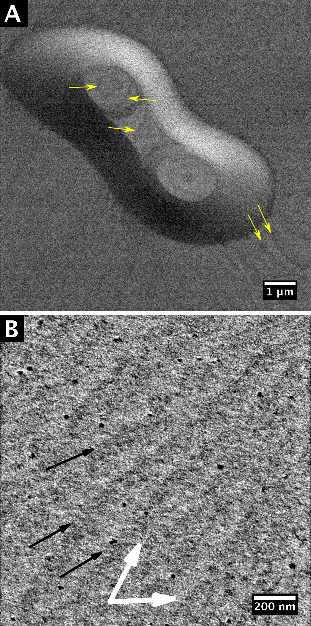
low magnification images of the Ag/Pt(111) sample surface recorded by LEEM and HIM are shown. The clean Pt(111) is occasionally decorated by mounds which sometimes originate from screw dislocations. These mounds are present on the clean Pt(111) surface and are neither formed nor affected by the subsequent Ag deposition. Representative examples of such surface mounds are presented in fig. 1. These mounds occur after annealing and a relatively swift cooling due to surface–bulk mass exchange [35]. The dark lines (a few marked by yellow arrows) in fig. 1(A) and 1(B) are steps separating atomically flat terraces. Mounds and step bunches are typically accompanied by wide terraces like in the top half of the image in fig. 1(A): Step migration during the annealing stage is suppressed by the mounds giving rise to step bunching and, at the same time, to wider terraces away from the obstruction caused by the mound. The mounds are threefold symmetric as becomes evident by looking at the relative lengths of the edge segments: opposite sides have different lengths, in other words mirror symmetry is absent. Moreover, adjacent facets of the mound have different brightnesses as is seen clearly in figs. 1(A) and 1(B). Unfortunately, field distortions [36] prevent a full structural characterization of the mounds by LEEM. Still we can extract important information. Steps along azimuthal directions on fcc (111) surfaces are different. They either have (111) or (001) type microfacets of which the former are energetically favoured [37]. The longer mound edges on opposing sides are apparently energetically favoured and from that fact we can derive that the brighter sides of the mounds are of the –(111) (oriented microfacets) type, while the darker sides in between are of the –(100) type. The threefold symmetry allows us to determine fully the orientation of the mounds in a field free situation such as in HIM. The curved dark line on top of t he mound represents a monatomic step (marked by yellow arrows in fig. 1(B)) as we conclude from the clear correspondence with the data in ref. 35 and references therein.
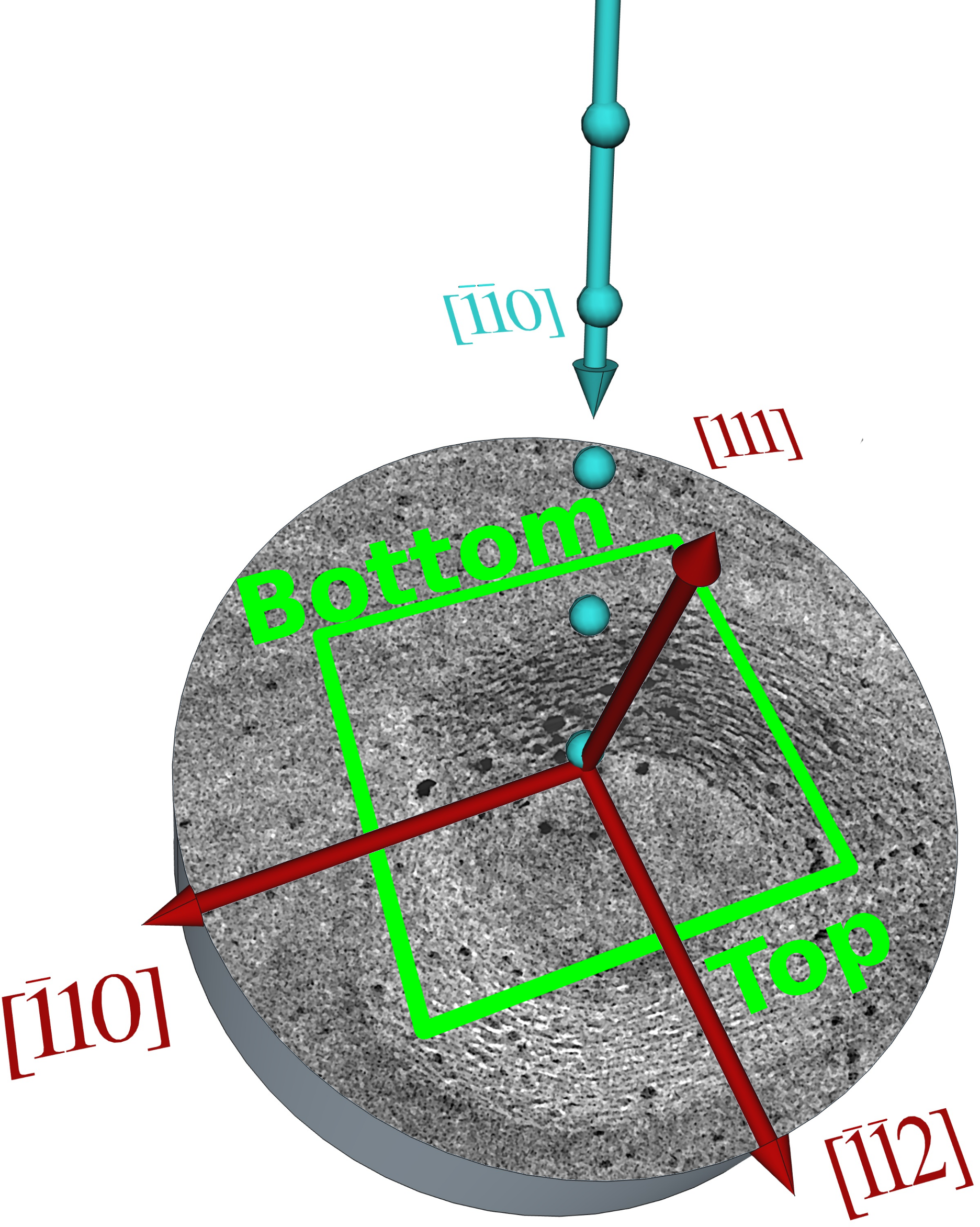
The appearance of such mounds in HIM can be seen from figs. 1(C) and 1(D). A low magnification image of a mound is presented in fig. 1(C). Note that there is no defined correspondence of the azimuth directions in the LEEM and the HIM data. A higher magnification of the mound sidewall is shown in fig. 1(D). Using HIM images as the one presented in fig. 1(C) and fig. 1(D) the orientation of the sample with respect to the beam can be determined. While in the center right part of fig. 1(D) straight step bunches are visible (terminated by facets), irregular and curved step bunches are visible at the top and bottom of the image. The straight step bunches are preferential oriented parallel to the directions of the Pt(111) sample surface. Using these step bunches the sample has been aligned with the He+ beam parallel to the direction and parallel to the Pt plane. The direction of the arrows in fig. 1(C) corresponds to the surface projection () of the surface normals of the less abundant facets. Obviously the dominant {111} oriented step facets are situated just in between. In this channelling condition the interaction of the primary beam with the sample is minimized and results in a low SE yield [26]. As a result the direction—except for a small alignment error—is pointing from left to right in the subsequent HIM images. As we will see further below, the achieved alignment is as good as perfect. The geometrical relationship between the primary He beam, the tilted sample and the crystallographic directions on the surface is outlined in fig. 2.
3.2 HIM analysis
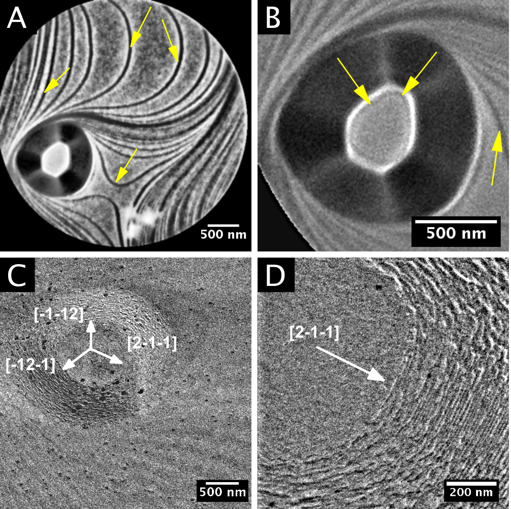
In the low magnification HIM image presented in fig. 3(A)
two mounds that originate from a twinned screw dislocation can be seen. The dislocation loop intersects the surface at the centers of the mounds. On the top of the mound dark bands can be seen. These dark bands have the typical appearance of growth steps usually also found at the top of such mounds. In the valley the lines meet and annihilate (see top of triangles) this can only be explained by a set of coupled screw dislocations with opposite rotation sense. The same contrast variation can also be observed at the surface surrounding the mounds (see for example the right side of fig. 3(A) and fig. 1(C)) where micrometer sized terraces are often observed (compare also fig. 1(A) for a LEEM image of a stepped surface). In fig. 3(B) a high resolution HIM image is presented obtained from the flat surface of the Ag/Pt(111) area surrounding the mound. An alternating arrangement of dark and bright bands can be observed. The and directions are indicated by a white arrows. Ideally steps run along directions. However, due to local curvature variations of the macroscopic surface or the presence of, e.g., mounds they may show quite severe deviations (see figs. 1(A) and 1(B)). Here the steps run diagonally, close to the direction but not exactly along it.
The second layer of the alloy consists, according to Secondary Ion Mass Spectroscopy [24] measurements, of 22% Pt atoms in a silver matrix. The constituent of the third layer is mainly Ag. Characteristically the third layer propagates by step edges, forming a periodically undulated sawtooth–shaped growth front [38]. Although the shape of the growth front is not clearly discernible in fig. 3(B) the black arrows indicate the possible location of the single atom high step edges. This is based on the fact that the Ag rich area starts to grow from ascending step edges [17, 38]. This example illustrates that the observation of atomic steps with HIM is not always straightforward for reasons not fully understood yet. In this case the discern of the steps is attributed to (small) differences in the work function of the second and the third layer [38].
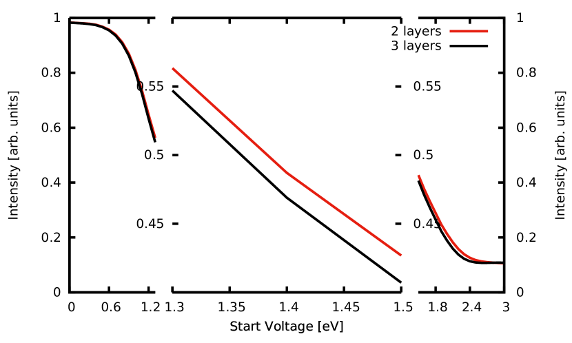
The measurement of the relative surface work-function (WF) with LEEM can be achieved with high lateral resolution by measuring the local brightness variation from a set of images recorded at different start voltages. At a very low start voltage, the probing electrons undergo total reflection (mirror mode imaging) [33, 34] resulting in uniformly bright images. With increase of the start voltage a sharp decrease in the reflected intensity is observed as electrons have enough energy to overcome the potential barrier and interact with the sample. The value of this critical voltage is a local measure of the surface WF. To measure the difference of the surface WF between two regions, sets of LEEM images as a function of the start voltage were recorded. The in fig. 4 presented bright field intensity versus electron voltage (I–V) curve was extracted for each pixel from the obtained sets.
Following the approach discussed above a work function difference between the dark and the bright bands of 25 meV has been obtained (see fig. 4). The dark spots visible in figs. 3(B,C) are attributed to platinum precipitates found in the Ag/Pt surface alloy layer.
Increasing the magnification further reveals more features of the sample surface. The FOV covers about three or four terraces each of them about 100 nm wide. Three sets of parallel lines running almost horizontally and under 120° can be seen in the HIM image presented in fig. 5(A) and (C) (A set of lines under the observed orientation is placed in the lower left corner to help the reader). An FFT of the image is provided in fig. 5(B).
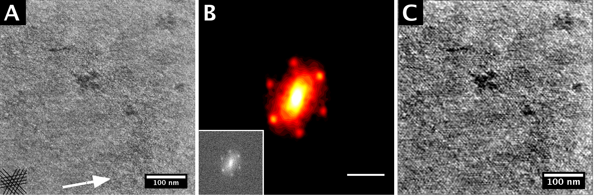
Correcting the vertical distortion—which will be discusses later—a 6 fold symmetric pattern can be observed. A custom made FFT filter101010A mask based on the FFT presented in fig. 5(B) has been used as a bandpass filter in the fourier space leaving only the frequencies of interest. The remaining FFT has than been converted back into real space to obtain fig. 5(C). based on fig. 5(B) has been used to create the contrast enhanced version of fig. 5(A) presented in fig. 5(C). The spacing of the spots in the FFT is at 6.65 nm0.08 nm after applying the necessary correction due to the tilt of the sample in the vertical direction (see below for further discussion). From the orientation of the spot pattern it is clear that this distance is along the set of directions. Please note that both the white arrow in fig. 5(A)—indicating the direction—as well as the FFT pattern in fig. 5(B) are slightly rotated off the horizontal due to a small azimuthal misalignment of the sample (please see fig. 2 for a sketch of the used imaging geometry). This azimuthal misalignment amounts to only 3.6°. Not only the misalignment of the azimuthal angle but also the possible misalignment of the polar angle of incidence of the ion beam can be checked quantitatively. The vertical distortion is a direct result of the off-normal direction of the beam (polar angle ). As a consequence the ion beam travels a longer distance upon applying a deflection voltage in the plane of incidence than upon applying the same voltage perpendicular to the plane of incidence by a factor of . This makes the in–plane dimensions of the structures seem shorter by a factor of . Obviously, in reciprocal space the pattern gets expanded in the vertical direction as is the case in fig. 5(B). Since the off–normal incidence of the ion beam is the only factor that could destroy the threefold symmetry of the image one can restore the symmetry by shrinking the vertical axis by . An optimal symmetry is obtained for =36.9°–38.6°, i.e. only 1.6°–3.3° off the ideal angle. We conclude that the realized alignment is excellent. However, due to the relatively low beam energy of 30 keV the acceptance angle for channeling is sufficiently large to allow for an effective channeling through the first few nanometers [26].
3.3 AFM data
AFM data of a mound, recorded ex–situ after the deposition of 3 layers of Ag, are presented in fig. 6.
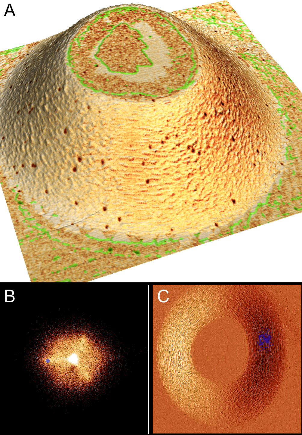
The 3D representation of the topography data, shown in fig. 6(a), is shaded using the phase signal. It confirms the HIM and LEEM observations. The mound and its surrounding are decorated by small black spots. They are attributed to the platinum–rich precipitates also visible in HIM and LEEM images (see fig. 3(B)–(C) for comparison) as dark objects. Formation of those precipitates was observed in previous investigations [39, 38] upon completion of the first layer, and were identified there, as few atoms high Pt clusters embedded in the surrounding. The clusters become less abundant but persist on the surface until a few tens of Ångström of Ag are deposited. The key observation from the data presented in fig. 6(a) is that the top of the mound shows regions corresponding to two different phases. One is the area appearing dark in the AFM phase data which occupies the center and rim area of the mound, the other phase is represented in white and found in between the dark areas. The fact that we can observe Pt clusters embedded in both types of regions, means that both regions correspond to at least one layer of the alloy. The observed step and terrace pattern on top of the mound is quite characteristic for the growth of the first few layers of Ag/Pt(111) [39, 38]. The higher coverage on top of the mound is explained by steering induced flux enhancement at protrusions [40]. The diffuse border separating the bright (Pt–rich) area from the outer dark (Ag–rich) area represents the growth front of the surface alloy. In figure 6(b) the slope distribution is presented. The slope distribution graph plots the local derivative of the surface and creates a 2D histogram from it [41]. The hexagonal shape of the mound is visible if one looks at the overall shape of the distribution. The three spokes that can be seen at 1, 5 and 9 o’clock represent areas with equal orientation in a very narrow azimuth angle band (1°). These are the regular step bunches that are straight and not curved. They can also be seen in the amplitude image (fig. 6(c)). There small bands of straight steps can be seen at 3, 7, and 11 o’clock. These straight step segments are responsible for the spokes in the slope distribution. In these areas the polar angle changes slightly (at the top and bottom of the mound, giving rise to the spoke in fig. 6(b)) but the azimuth angle is constant. As an example the facets at the 3 o’clock side of the mound are highlighted in both figures (7° polar, 3.7° azimuth 0.25°). This is one of the directions. The straight steps run parallel to one of the directions.
4 Discussion and conclusions
Helium Ion Microscopy is well known for its surface sensitivity [10]. The usually obtained SE images are sensitive to small variations in work function [42, 11, 4]. Both effects are related to the particularities of the SE generation in HIM [43, 7]. The work function difference (see fig. 4) between the platinum rich (dark) and silver rich (bright) areas (see fig. 3(A)–(B)) is only 25 meV. This is a remarkable example for both the surface sensitivity as well as the susceptibility of the method to changes in the work function. Although the steps can not be seen directly from the morphology this is the first visualization of a single atomic layer high steps in a SE HIM image. Previous—topography based—images of steps [4] are obtained from materials with large unit cells where each step is several atoms high.
The results presented in fig. 5 are a demonstration of the applicability of the dechanneling contrast [11]. The 2 layers Ag on Pt(111) system is characterized by a stress induced triangular network of dislocations originating from the interface. These dislocations separate areas in the first two layers which are shifted along the [] direction over of the nearest neighbour distance. Locally, this leads to a different stacking of the layers as compared to the bulk fcc stacking. In fig. 7(A) a side view of the simplified atomic structure is presented. This is not the actual atomic structure of Ag/Pt system but should clarify why we can obtain contrast on such a surface. For a more accurate description of the atomic model the reader is referred to ref. 24.
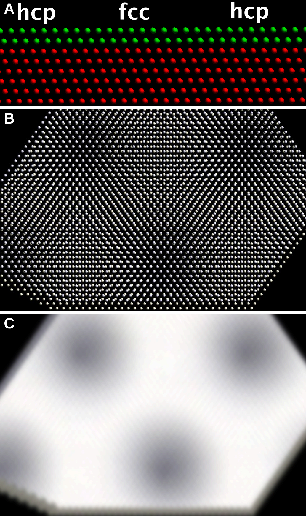
In this projection the first two layers are comprised of 23 Ag atoms while the underlying bulk Pt contains 24 atoms over the same distance. As a consequence a fcc stacking is observed in the center of the image while a hcp stacking is observed at the left and right side. In the latter areas the silver atoms suppress axial channeling of the helium ions into the Pt. A detailed characterization of this system with respect to the surface can be found in [25, 24]. Using the step bunches on the mounds (see fig. 1(C) and (D)) the sample has been aligned azimuthally with the direction roughly parallel to the tilt axis direction. Using a tilt of 35° the substrate has been oriented in a channeling direction for the incoming He+ beam. In hcp areas the top two atomic layers of the surface are shifted by two thirds of the inter chain spacing leading to local CAC (hcp) stacking in stead of local ABC (fcc) stacking. This closes the channel and results in an increased scattering probability. In fig. 7(B) the view of the beam on the atomic structure is presented. The 6–fold symmetric arrangement of the fcc channeling areas is visible. Subsequently, a higher SE yield is obtained in such hcp areas compared to the fcc areas with a lower scattering probability. A qualitative representation of the expected SE yield is presented in fig. 7(C). The value of 6.65 nm0.08 nm for the periodicity of the surface pattern is in excellent agreement with the 6.55 nm measured by SPA–LEED [25]. Both values correspond to the distance between parallel base vectors of the super cell. The numbers show that the calibration of the HIM is correct to about 1%. The obtained periodicity of 6.65 nm agrees with a situation in which 23 Ag–atoms in the top–layer reside on 24 Pt lattice sites to an accuracy of 0.03%. Rightfully we can and do claim that we reach atomic precision here. We do not claim atomic resolution, since that would require the imaging of individual atoms. We like to suggest, however, that it is possibly not the instrument’s limitation but rather insufficient atomic contrast which prevents atomic resolution.
In summary we have—to the best of our knowledge—for the first time visualized single atom high surface steps using Helium Ion Microscopy. The contrast is based on minute changes of the work function across the otherwise atomically flat terraces. In addition we used the dechanneling contrast mechanism to successfully visualize the periodic arrangement of fcc and hcp regions in a 2–3 layers thick surface film. This pattern is the result of a triangular dislocation network at the interface between the silver alloy layer and the platinum bulk. The contrast in HIM is the result of a lateral displacement of the outermost film layers over a nearest neighbour distance divided by along a direction. The measured periodicity of 6.65 nm and the fact that the contrast is based on channeling/dechanneling confirms in detail earlier measurements using other methods. The obtained results are powerful demonstrations of the surface sensitivity and high resolution capabilities of the Helium Ion Microscopy.
Acknowledgements
We want to thank Robin Berkelaar for acquiring the AFM data. This work is part of ECHO research program 700.58.026, which is financed by the Chemical Sciences Division of the Netherlands Organisation for Scientific Research (NWO).
References
-
[1]
G. Hlawacek, V. Veligura, R. van Gastel, B. Poelsema,
Helium
ion microscopy, J. Vac. Sci. Technol. B Microelectron. Nanom. Struct.
32 (2) (2014) 020801.
arXiv:arXiv:1311.1711v1, doi:10.1116/1.4863676.
URL http://scitation.aip.org/content/avs/journal/jvstb/32/2/10.1116/1.4863676 -
[2]
D. C. Joy, Helium
Ion Microscopy, SpringerBriefs in Materials, Springer New York, New York,
NY, 2013.
doi:10.1007/978-1-4614-8660-2.
URL http://link.springer.com/10.1007/978-1-4614-8660-2 -
[3]
R. Hill, F. H. M. Rahman,
Advances
in helium ion microscopy, Nucl. Instruments Methods Phys. Res. Sect. A
645 (1) (2011) 96–101.
doi:10.1016/j.nima.2010.12.123.
URL http://linkinghub.elsevier.com/retrieve/pii/S0168900210029037 -
[4]
K. Buchholt, P. Eklund, J. Jensen, J. Lu, A. L. Spetz, L. Hultman,
Step-flow
growth of nanolaminate Ti$_3$SiC$_2$ epitaxial layers on
4H-SiC(0001), Scr. Mater. 64 (12) (2011) 1141–1144.
doi:10.1016/j.scriptamat.2011.03.013.
URL http://linkinghub.elsevier.com/retrieve/pii/S1359646211001357 -
[5]
H. Zhang, Y. Miyamoto, A. Rubio,
Ab initio
Simulation of Helium-Ion Microscopy Images: The Case of Suspended Graphene,
Phys. Rev. Lett. 109 (26) (2012) 265505.
doi:10.1103/PhysRevLett.109.265505.
URL http://link.aps.org/doi/10.1103/PhysRevLett.109.265505 -
[6]
B. W. Ward, J. A. Notte, N. P. Economou,
Helium ion
microscope: A new tool for nanoscale microscopy and metrology, J. Vac. Sci.
Technol. B 24 (6) (2006) 2871.
doi:10.1116/1.2357967.
URL http://scitation.aip.org/getabs/servlet/GetabsServlet?prog=normal{&}id=JVTBD9000024000006002871000001{&}idtype=cvips{&}gifs=yeshttp://link.aip.org/link/?JVB/24/2871http://link.aip.org/link/JVTBD9/v24/i6/p2871/s1{&}Agg=doi -
[7]
Y. V. Petrov, O. F. Vyvenko,
Secondary
electron emission spectra and energy selective imaging in helium ion
microscope, in: J. T. Thomas, D. D. Desjardins, J. J. Güell, K. L.
Bernier (Eds.), Proc. SPIE, Vol. 8036, SPIE, Orlando, Florida, 2011, pp.
80360O–1–80360O–10.
doi:10.1117/12.886347.
URL http://proceedings.spiedigitallibrary.org/proceeding.aspx?articleid=1265199 -
[8]
J. Cazaux,
Calculated
influence of work function on SE escape probability and Secondary Electron
Emission yield, Appl. Surf. Sci. 257 (3) (2010) 1002–1009.
doi:10.1016/j.apsusc.2010.08.007.
URL http://linkinghub.elsevier.com/retrieve/pii/S0169433210010664 -
[9]
Y. Lin, D. C. Joy, A new
examination of secondary electron yield data, Surf. Interface Anal. 37 (11)
(2005) 895–900.
doi:10.1002/sia.2107.
URL http://doi.wiley.com/10.1002/sia.2107 -
[10]
G. Hlawacek, I. Ahmad, M. A. Smithers, E. S. Kooij,
To see or not to see: Imaging
surfactant coated nano-particles using HIM and SEM., Ultramicroscopy 135C
(2013) 89–94.
arXiv:1304.7167,
doi:10.1016/j.ultramic.2013.07.010.
URL http://arxiv.org/abs/1304.7167http://linkinghub.elsevier.com/retrieve/pii/S0304399113001964http://www.ncbi.nlm.nih.gov/pubmed/23948627 -
[11]
G. Hlawacek, V. Veligura, S. Lorbek, T. F. Mocking, A. George, R. van Gastel,
H. J. W. Zandvliet, B. Poelsema,
Imaging
ultra thin layers with helium ion microscopy: Utilizing the channeling
contrast mechanism., Beilstein J. Nanotechnol. 3 (2012) 507–512.
doi:10.3762/bjnano.3.58.
URL http://www.pubmedcentral.nih.gov/articlerender.fcgi?artid=3458595{&}tool=pmcentrez{&}rendertype=abstract - [12] E. Bauer, LEEM Basics, Surf. Rev. Lett. 5 (6) (1998) 1275–1286.
-
[13]
M. Whangbo, G. Bar, R. Brandsch,
Qualitative
relationships describing height and phase images of tapping mode atomic force
microscopy. An application to micro-contact-printed patterned self-assembled
monolayers, Appl. Phys. A 66 (0) (1998) 1267–1270.
doi:10.1007/s003390051340.
URL http://www.springerlink.com/content/mypd44hpwblwjdjd - [14] I. Schmitz, M. Schreiner, G. Friedbacher, M. Grasserbauer, Phase imaging as an extension to tapping mode AFM for the identification of material properties on humidity-sensitive surfaces, Appl. Surf. Sci. 115 (96) (1997) 190–198. doi:10.1016/S0169-4332(97)80204-8.
- [15] R. Garcia, R. Magerle, R. Perez, Nanoscale compositional mapping with gentle forces, Nat. Mater. 6 (2007) 405–411.
-
[16]
A. F. Becker, G. Rosenfeld, B. Poelsema, G. Comsa,
Two-dimensional
microstructures of submonolayer Ag on Pt (111) induced by elastic strain,
Phys. Rev. Lett. 70 (4) (1993) 477.
URL http://journals.aps.org/prl/abstract/10.1103/PhysRevLett.70.477 -
[17]
H. Röder, R. Schuster, H. Brune, K. Kern,
Monolayer-confined
mixing at the Ag-Pt (111) interface, Phys. Rev. Lett. 71 (13) (1993) 2086.
URL http://journals.aps.org/prl/abstract/10.1103/PhysRevLett.71.2086 -
[18]
U. Strüber, J. Küppers,
Spectroscopic
confirmation of STM derived Ag/Pt mixing in annealed Ag submonolayers at Pt
(111) surfaces, Surf. Sci. Lett. 294 (1) (1993) L924—-L928.
URL http://www.sciencedirect.com/science/article/pii/0167258493911166 -
[19]
P. Zeppenfeld, M. A. Krzyzowski, C. Romainczyk, R. David, G. Comsa,
H. Röder, K. Bromann, H. Brune, K. Kern,
Stability
of disk and stripe patterns of nanostructures at surfaces, Surf. Sci.
342 (1) (1995) L1131—-L1136.
URL http://www.sciencedirect.com/science/article/pii/0039602895008918 -
[20]
J. Tersoff,
Surface-confined
alloy formation in immiscible systems, Phys. Rev. Lett. 74 (3) (1995) 434.
URL http://journals.aps.org/prl/abstract/10.1103/PhysRevLett.74.434 -
[21]
M. Jankowski, H. Wormeester, H. J. W. Zandvliet, B. Poelsema,
Desorption
of oxygen from alloyed Ag/Pt (111), J. Chem. Phys. 140 (23) (2014) 234705.
URL http://scitation.aip.org/content/aip/journal/jcp/140/23/10.1063/1.4882906 -
[22]
H. Brune, H. Röder, C. Boragno, K. Kern,
Strain relief
at hexagonal-close-packed interfaces., Phys. Rev. B. Condens. Matter 49 (4)
(1994) 2997–3000.
URL http://www.ncbi.nlm.nih.gov/pubmed/10011151http://journals.aps.org/prb/abstract/10.1103/PhysRevB.49.2997 -
[23]
A. Bendounan, J. Braun, J. Minár, S. Bornemann, R. Fasel,
O. Gröning, Y. Fagot-Revurat, B. Kierren, D. Malterre, F. Sirotti,
Others, H. Ebert, Monitoring
the formation of interface-confined mixture by photoelectron spectroscopy,
Phys. Rev. B 85 (24) (2012) 245403.
doi:10.1103/PhysRevB.85.245403.
URL http://link.aps.org/doi/10.1103/PhysRevB.85.245403http://journals.aps.org/prb/abstract/10.1103/PhysRevB.85.245403 -
[24]
K. Aït-Mansour, H. Brune, D. Passerone, M. Schmid, W. Xiao, P. Ruffieux,
A. Buchsbaum, P. Varga, R. Fasel, O. Gröning,
Interface-confined
mixing and buried partial dislocations for Ag bilayer on Pt(111), Phys.
Rev. B 86 (8) (2012) 085404.
doi:10.1103/PhysRevB.86.085404.
URL http://link.aps.org/doi/10.1103/PhysRevB.86.085404 -
[25]
M. Jankowski, H. Wormeester, H. J. W. Zandvliet, B. Poelsema,
Temperature-dependent
formation and evolution of the interfacial dislocation network of
Ag/Pt(111), Phys. Rev. B 89 (23) (2014) 235402.
doi:10.1103/PhysRevB.89.235402.
URL http://link.aps.org/doi/10.1103/PhysRevB.89.235402 -
[26]
V. Veligura, G. Hlawacek, R. van Gastel, H. J. W. Zandvliet, B. Poelsema,
Channeling
in helium ion microscopy: Mapping of crystal orientation., Beilstein J.
Nanotechnol. 3 (2012) 501–506.
doi:10.3762/bjnano.3.57.
URL http://www.pubmedcentral.nih.gov/articlerender.fcgi?artid=3458595{&}tool=pmcentrez{&}rendertype=abstracthttp://www.pubmedcentral.nih.gov/articlerender.fcgi?artid=3458594{&}tool=pmcentrez{&}rendertype=abstract -
[27]
R. van Gastel, L. Barriss, C. A. Sanford, G. Hlawacek, L. Scipioni, A. Merkle,
D. Voci, C. Fenner, H. J. W. Zandvliet, B. Poelsema,
Design and
performance of a Near Ultra High Vacuum Helium Ion Microscope, Microsc.
Microanal. 17 (S2) (2011) 928–929.
doi:10.1017/S1431927611005514.
URL http://journals.cambridge.org/action/displayAbstract?fromPage=online{&}aid=8396961http://www.journals.cambridge.org/abstract{_}S1431927611005514 -
[28]
R. van Gastel, G. Hlawacek, H. J. Zandvliet, B. Poelsema,
Subsurface
analysis of semiconductor structures with helium ion microscopy,
Microelectron. Reliab. 52 (9-10) (2012) 2104–2109.
doi:10.1016/j.microrel.2012.06.130.
URL http://linkinghub.elsevier.com/retrieve/pii/S0026271412003277 -
[29]
S. Sijbrandij, J. A. Notte, L. Scipioni, C. Huynh, C. A. Sanford,
Analysis and
metrology with a focused helium ion beam, J. Vac. Sci. Technol. B 28 (1)
(2010) 73.
doi:10.1116/1.3271254.
URL http://link.aip.org/link/JVTBD9/v28/i1/p73/s1{&}Agg=doi -
[30]
G. Behan, J. F. Feng, H. Z. Zhang, P. N. Nirmalraj, J. J. Boland,
Effect of
sample bias on backscattered ion spectroscopy in the helium ion microscope,
J. Vac. Sci. Technol. A 28 (6) (2010) 1377.
doi:10.1116/1.3502667.
URL http://link.aip.org/link/JVTAD6/v28/i6/p1377/s1{&}Agg=doi -
[31]
V. Veligura, G. Hlawacek, U. Jahn, R. van Gastel, H. J. W. Zandvliet,
B. Poelsema,
Creation
and physical aspects of luminescent patterns using helium ion microscopy,
J. Appl. Phys. 115 (18) (2014) 183502.
doi:10.1063/1.4875480.
URL http://scitation.aip.org/content/aip/journal/jap/115/18/10.1063/1.4875480 -
[32]
S. A. Boden, T. M. W. Franklin, L. Scipioni, D. M. Bagnall, H. N. Rutt,
Ionoluminescence in the
helium ion microscope., Microsc. Microanal. 18 (6) (2012) 1253–1262.
doi:10.1017/S1431927612013463.
URL http://www.ncbi.nlm.nih.gov/pubmed/23237545 -
[33]
R. M. Tromp, M. C. Reuter,
Imaging
with a low-energy electron microscope, Ultramicroscopy 50 (2) (1993)
171–178.
URL http://www.sciencedirect.com/science/article/pii/030439919390007K -
[34]
E. Bauer, Low
energy electron microscopy, Reports Prog. Phys. 57 (9) (1994) 895–938.
doi:10.1088/0034-4885/57/9/002.
URL http://iopscience.iop.org/0034-4885/57/9/002http://stacks.iop.org/0034-4885/57/i=9/a=002?key=crossref.6221823104b9f60edd0744014b69df50 - [35] B. Poelsema, J. B. Hannon, N. C. Bartelt, G. L. Kellogg, Bulk-surface vacancy exchange on Pt ( 111 ), Appl. Phys. Lett. 111 (2012) 2551. doi:10.1063/1.1695434.
-
[36]
S. A. Nepijko, N. N. Sedov, G. Schönhense,
Peculiarities
of imaging one-and two-dimensional structures using an electron microscope in
the mirror operation mode, J. Microsc. 203 (3) (2001) 269–276.
URL http://onlinelibrary.wiley.com/doi/10.1046/j.1365-2818.2001.00895.x/full - [37] T. Michely, G. Comsa, Temperature dependence of sputtering morphologies of Pt(111), Surf. Sci. 256 (1991) 217—-226.
-
[38]
M. Jankowski,
Reciprocal and
reap space investigation of Ag/Pt(111) : growth, structure and interaction
with Oxygen (sep 2014).
doi:10.3990/1.9789036537186.
URL http://purl.org/utwente/doi/10.3990/1.9789036537186 - [39] E. van Vroonhoven, Remarkable Interface Activity: A LEEM Study of Ge(001) and Ag/Pt(111) at High Temperatures, Ph.D. thesis, University of Twente (2005).
- [40] S. van Dijken, L. C. Jorritsma, B. Poelsema, Steering enhanced roughness during metal deposition at grazing incidence, Phys. Rev. Lett. 82 (1999) 4038.
-
[41]
P. Klapetek, D. Necas, C. Anderson,
Gwyddion user
guide (jun 2015).
URL http://gwyddion.net/documentation/user-guide-en/ -
[42]
A. George, M. Knez, G. Hlawacek, D. Hagedoorn, H. H. J. Verputten, R. van
Gastel, J. E. ten Elshof, Nanoscale patterning of
organosilane molecular thin films from the gas phase and its applications:
fabrication of multifunctional surfaces and large area molecular templates
for site-selective material deposition., Langmuir 28 (5) (2012) 3045–3052.
doi:10.1021/la204437r.
URL http://pubs.acs.org/doi/abs/10.1021/la204437rhttp://www.ncbi.nlm.nih.gov/pubmed/22229783 -
[43]
K. Ohya, T. Yamanaka, K. Inai, T. Ishitani,
Comparison
of secondary electron emission in helium ion microscope with gallium ion and
electron microscopes, Nucl. Instruments Methods Phys. Res. Sect. B 267 (4)
(2009) 584–589.
doi:10.1016/j.nimb.2008.11.003.
URL http://linkinghub.elsevier.com/retrieve/pii/S0168583X08012548