Tunneling in Graphene-Topological Insulator Hybrid Devices
Abstract
Hybrid graphene-topological insulator (TI) devices were fabricated using a mechanical transfer method and studied via electronic transport. Devices consisting of bilayer graphene (BLG) under the TI Bi2Se3 exhibit differential conductance characteristics which appear to be dominated by tunneling, roughly reproducing the Bi2Se3 density of states. Similar results were obtained for BLG on top of Bi2Se3, with 10-fold greater conductance consistent with a larger contact area due to better surface conformity. The devices further show evidence of inelastic phonon-assisted tunneling processes involving both Bi2Se3 and graphene phonons. These processes favor phonons which compensate for momentum mismatch between the TI and graphene points. Finally, the utility of these tunnel junctions is demonstrated on a density-tunable BLG device, where the charge-neutrality point is traced along the energy-density trajectory. This trajectory is used as a measure of the ground-state density of states.
pacs:
73.40.Gk, 73.50.-h, 73.20.AtIn topological insulators (TIs), the protected surface state is bound to the interface between materials with different bulk topological invariants Hasan_Kane_2010 . Although the surface state will remain gapless as long as the symmetries protecting the bulk topological invariant are retained, its dispersion and location depend on the band-structures of the two interfacing materials. A model system allowing the investigation of such interface properties is the graphene-TI hybrid, where graphene resides in immediate proximity to the TI, separating it from the vacuum or from another trivial dielectric. Indeed, as part of a 3D continuum, graphene is topologically trivial. However, with a significant spin-orbit (SO) term, graphene could become a 2D TI Kane_Mele_2005 .
Recent studies Jin_2013 ; Liu_2013 ; Kou_2013 ; Zhang_Rossi_2014 which theoretically investigate the properties of such hybrids, generally assume that the graphene and TI bands couple strongly, leading to fundamental modifications to the graphene band structure, which is expected to inherit an enhanced SO coupling Jin_2013 and attain non-trivial spin-textures Zhang_Rossi_2014 . When sandwiched between two ultra thin layers of Bi2Se3, the graphene layer may become a 2D TI Kou_2013 . However, as the surface states of TIs such as Bi2Se3 are centered at the point in -space, they should be prevented by momentum conservation from hybridizing with the graphene bands, centered at the points. This difficulty is often resolved theoretically by assuming that periodicity at the interface would cause the graphene Brillouine zone (BZ) to fold Jin_2013 ; Liu_2013 ; Kou_2013 ; Zhang_Rossi_2014 , bringing significant spectral weight to the point.
Here we present an experimental study of graphene-TI hybrid devices fabricated using a mechanical transfer technique Dean_hBN_2010 which allows the fabrication of vertical heterostructures involving a wide variety of van-der-Waals materials. In our devices, which consist of either monolayer (MLG) or bilayer graphene (BLG) stacked above or below the TI Bi2Se3, the graphene and TI layers are weakly coupled, with transport between them governed by tunneling. The devices reveal a rich inelastic spectrum consisting of graphene and Bi2Se3 phonons. Finally, we demonstrate the utility of the interface tunnel-junction to probe the density-dependent evolution of spectral features in BLG.
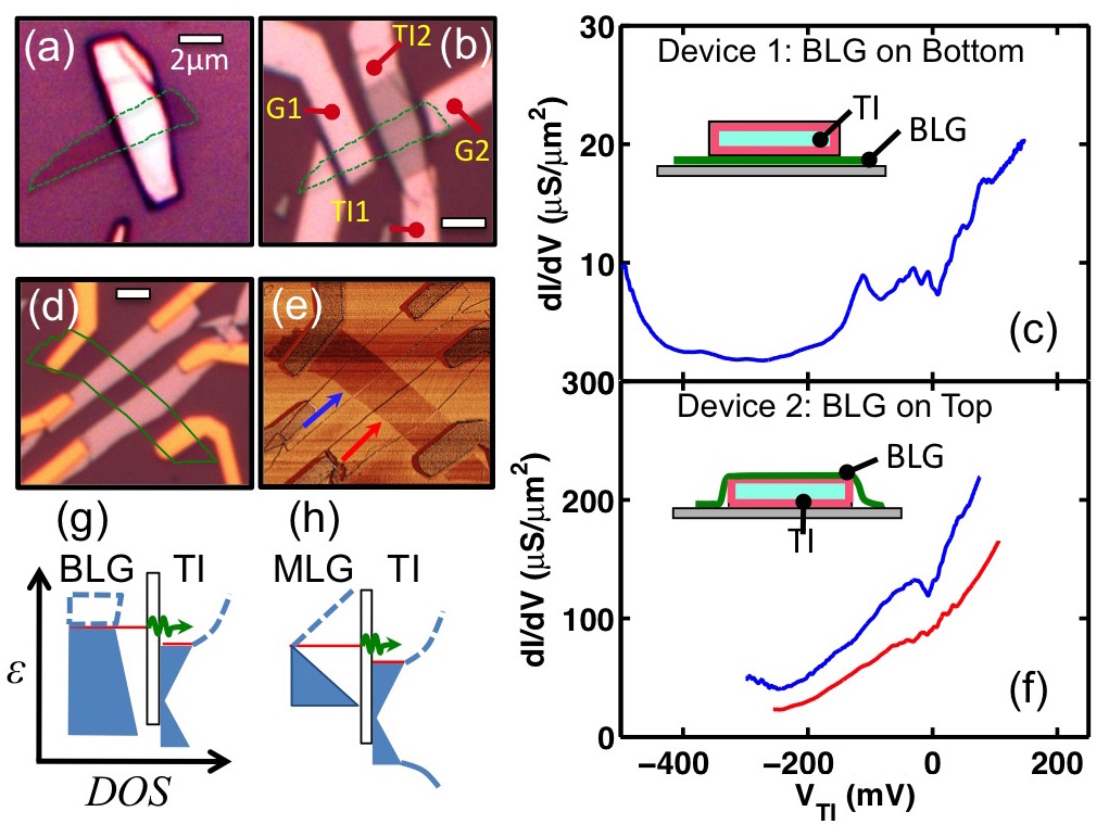
Fig. 1(a) shows Device 1, where a Bi2Se3 flake is transferred on top of a BLG flake (outlined in green) deposited on SiO2. The flakes are independently contacted by evaporated metallic electrodes (Fig. 1(b)). The BLG-TI junctions are studied by measuring the differential conductance vs. applied bias voltage with the source on one material and the drain on the other (TI1 to G1). A four-probe geometry is realized by measuring the voltage across the opposing contacts ( = V(TI2)-V(G2)). The trace at of Device 1 (Fig. 1(c)) shows a pronounced suppression at negative values, similar to STM measurements taken on Bi2Se3 Alpichshev_2012 ; Cheng_LL_MBE_2010 ; Hanaguri_2010 , where is proportional to the density of states (DOS) and the suppression at negative bias is associated with the bulk gap of the Bi2Se3. The BLG-TI interface therefore behaves as an effective tunnel junction although no intentional barrier was placed between the materials. It is a remarkably robust junction, maintaining a stable signal while sustaining high voltage biases exceeding 0.5 V at negative bias.
The tunneling functionality of the graphene-Bi2Se3 interface could be a consequence of Bi2Se3 oxidation Kong_Oxidation_2011 . In over 20 devices studied, the interface resistance varied from 10 M to 10 , which could be associated with varying degrees of oxidation. The stability and high bias achieved by graphene-TI junctions, however, do not favor this explanation – oxide-based junctions rarely function at biases in excess of 200 meV Tsui_1970 . Alternatively, the variation in interface resistance could arise due to differences in the effective contact area: graphene conforms to the underlying substrate and has angstrom-scale height variations when deposited on SiO2 resulting in an effective partial contact area. To test this we studied devices where BLG is deposited on top of Bi2Se3: in Device 2 a single BLG flake covers two Bi2Se3 flakes (Fig. 1(d-e)). Measured separately (red and blue curves in panel (f)), the two junctions exhibit comparable characteristics which are very similar to the “graphene on bottom” devices (albeit with smaller bias range).
The interface conductivity of “graphene-on-top” junctions is an order of magnitude greater than “graphene on bottom” ones, indicating that the effective contact area is a plausible source of variation. It is not clear, however, what is the origin of the generic tunneling functionality. An interesting possibility is that the tunnel barrier is associated with the lack of direct chemical bonding between the two layers. Inter-layer tunnel barriers in layered materials is observed in high Tc superconductors Kleiner_1994 and in vdW materials such as 4Hb- Wattamaniuk_1975 . Incoherent interlayer transport was also reported in stacked twisted bilayer graphene devices Kim_PRL_2013 , and graphene layers could be weakly coupled to underlying graphite Li_Andrei_2007 . Testing this hypothesis would require further investigation.
As expected, the characteristics vary with the choice of MLG vs. BLG. The tunneling current is expressed as a convolution of the graphene DOS and the TI DOS wolf_book
| (1) |
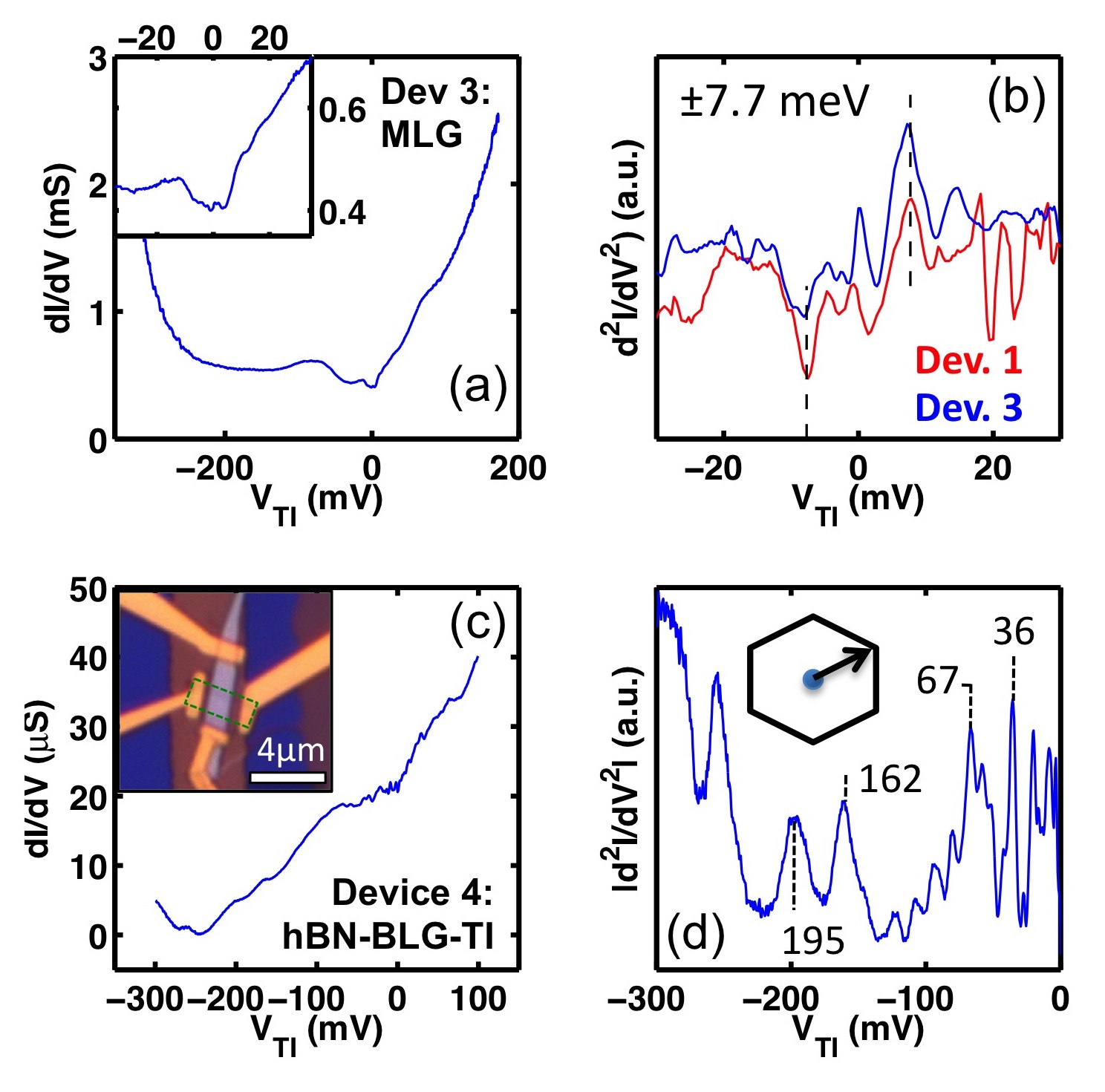
where is the effective overlap area and stands for the tunnel coupling through the barrier. This expression is qualitatively depicted in the schematics in Fig. 1(g,h), showing on the left and (including bulk and surface) on the right. For BLG devices (panel (g)) is relatively featureless and can be factored out of the integral, so the curve effectively probes . This explains why BLG-TI traces are similar to STM measurements of Bi2Se3, and suggests that BLG may be useful as a tunneling electrode for probing other vdW systems. MLG-TI devices (panel (h)) have energy-dependent on both sides of the barrier, and Device 3 (Fig 2(a)) indeed exhibits a very different characteristic, with a stronger suppression around zero-bias which we associate with the graphene Dirac point.
Tunnel junctions are useful in measuring inelastic spectra, where the onset of processes such as phonon-assisted tunneling appears as step-increase features in the differential conductance. These are detectable as peaks in the 2nd derivative at bias voltages corresponding to the phonon energies. It is possible to differentiate between Bi2Se3 and graphene phonons because their respective spectra span different energy ranges (up to 20 meV for Bi2Se3 Zhu_2011 , and up to 200 meV for graphene Wirtz_Rubio_2004 ). Several devices exhibit well-developed inelastic spectra: Device 3 (Fig. 2(a)), has sharp step-like features in close to zero (inset). The corresponding plot (Fig. 2(b)), shows peaks at 7.7 meV which coincide in Device 3 (MLG) and in Device 1 (BLG). We associate this feature with a Bi2Se3 surface optical phonon previously identified using Helium scattering at the same energy Zhu_Phonons_2012 . This phonon plays a role in suppressing surface transport Costache_2014 , and inelastic tunneling data may be useful in probing its coupling to surface electrons.
Signatures of graphene phonons, appearing at higher bias voltages, are found in numerous devices. For example, in Device 4 (Fig. 2(c,d)), a higher quality device fabricated by deposition of BLG on h-BN followed by transferring Bi2Se3 on top. The plot shows a prominent peak at 67 meV, corresponding to the energy of the graphene ZA/ZO mode at the points. This phonon is seen in many graphene and graphite tunneling experiments both in devices Amet_DGG_2012 and in STM Zhang_2008 ; Brar_2010 , and is generally believed to assist the tunneling process by providing the momentum required to inject an electron to the points. In our devices, where graphene and Bi2Se3 Fermi surface momenta are highly mismatched, it is likely that the same phonon is required to allow momentum-conserving tunneling from low energy Bi2Se3 states, centered at the point, to the graphene points (Schematic in inset to Fig. 2(d)). Device 4 also exhibits a feature at 162 meV associated with the LA/LO mode, also a phonon, and a feature at 195 meV associated with the TO mode at . Other features (e.g. a phonon at 36 meV) could be associated with the h-BN substrate Amet_DGG_2012 .
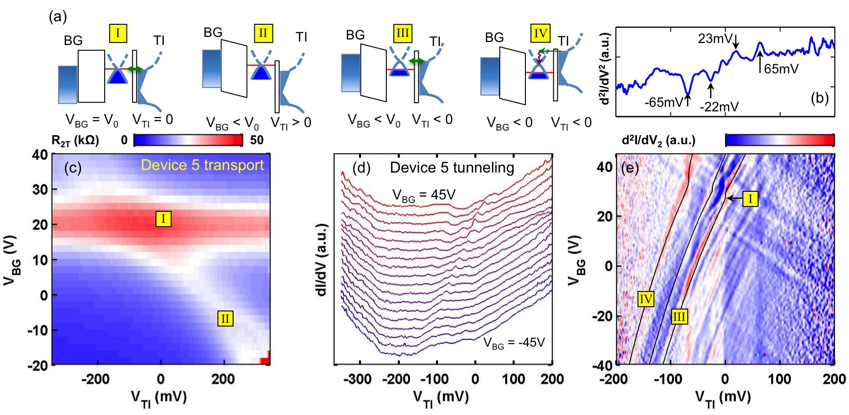
In the rest of this Letter we focus on Device 5, which has the same geometry as Device 1: TI on top of a density-tunable BLG flake. Device 5 can be measured by graphene in-plane transport (G1 to G2) or by tunneling (T1 to G1). In-plane resistance is presented in Fig. 3(c), showing a resistance peak when the chemical potential crosses the BLG CNP. The Bi2Se3 electrode acts as a well-behaved gate, and the small tunneling current does not interfere with the in-plane measurement. The resistance map is typical of doubly-gated graphene Huard2007 ; Thiti_PRL_2010 , where the diagonal feature corresponds to a high resistance state in the BLG region underneath the TI. This feature intercepts at , indicating that the BLG is p-doped and the CNP is energetically mismatched from the TI DP (Fig. 3(a) annotation I). Its slope is dictated by the requirement that the top and bottom gates compensate each other’s charge (annotation II) and therefore follows the ratio ( and are the graphene-TI and graphene-back gate capacitances, respectively). Using this relation, we extract the geometric capacitance of the TI-BLG junction , 110 times greater than the back-gate capacitance. Both the relative permittivity of the interlayer medium, , and the graphene-Bi2Se3 effective distance, , are unknown. However, the measured value of fixes their ratio to nm-1. As the interface is a tunnel junction, is unlikely to exceed nm, setting a limit of .
Gate-dependent tunneling measurements are presented in Fig. 3(d-e): Such measurements are sensitive to energy shifts in the spectral features due to the changes in density. In Fig. 3(d) it is clear that the underlying structure of the Bi2Se3 gap at negative is retained while a set of features closer to zero bias evolve with . To trace these features we plot the second derivative as a color map in Fig 3(e). The data exhibit a set of diagonal features with opposite slopes and gate-independent features which appear as faint vertical lines. The latter gate-independent features are enhanced by averaging over all back-gate values (Fig. 3(b)), where we again find the ZA/ZO phonon features at 65 meV. The 22 meV feature coincides with the energy of the Bi2Se3 phonon Zhu_2011 .
changes the graphene density, vertically shifting the band-structure (Fig. 3(a), annotation III). To trace a spectral feature such as the CNP, a voltage has to be applied to compensate for the density-induced change in chemical potential, . This is formulated as:
| (2) |
To trace spectral features on the - plane, we have to note that planar tunneling electrodes are large capacitors which charge the graphene layer at finite bias, as discussed earlier. The equations governing the charging of the graphene layer connect the incremental gate voltages to the incremental charges on the back-gate and TI :
| (3) |
where .
Interestingly the CNP tunneling condition in Eq. 2 also ensures that there will be no extra charge accumulated on the TI (), as the argument in parenthesis in Eq. 3 remains zero. More generally, this means that constant energy features lie on trajectories which keep the charge on the tunneling electrode fixed. In the Supplementary Information SI we derive the CNP-tunneling trajectory and find its slope to be:
| (4) |
where is the quantum capacitance of the BLG. The slope is independent of , consistent with the induced charge on the TI remaining zero.
As a result, Eq. 4 can be used to evaluate by fitting the slope of the features appearing in the figure. The most prominent feature in Fig. 3(e), marked by “III”, is likely the charge neutrality point, which attains a cusp in the DOS due to a finite displacement field (annotation I). The slope of this feature is not constant, and appears to vary along the trajectory (Fig. S1). This indicates that , and hence the DOS, changes with density, as expected for the hyperbolic dispersion of BLG DasSarmaReview_2011 ; CastroNeto_RMP_2009 ; McCann_BLG_2006 .
We fit the expected trajectory (Fig. 3(e), feature “III”). To calculate this fit it is crucial to acknowledge that the BLG dispersion varies within the plane, where at each point the displacement field is different. The calculation, described in the SI SI , is carried out self-consistently, using an approximate trajectory for calculating the displacement field at each value of and . We then extract , and finally and integrate the trajectory from the slope in Eq. 4. The calculation is refined iteratively. Using the Fermi velocity as a fitting parameter, the full trajectory can be reproduced with , in good agreement with non-interacting values for BLG.
Multiple replica (marked by IV in Fig. 3(e)) of the CNP tunneling feature, appear as lines running parallel to the elastic feature (“IV”). They are associated with phonon-assisted inelastic tunneling processes to the CNP. Unlike the gate-independent phonon-onset features discussed above, where tunneling takes place to the Fermi energy, these features represent phonon-assisted tunneling to some sharp spectral feature (here the CNP), and evolve with the gate in parallel to the elastic tunneling feature. Their trajectories, presented in Fig. S1, should depend on the elastic feature, after accounting for modified displacement fields at higher bias. However, to fit the actual data we find that the Fermi velocities have to be modified in each of the inelastic features (assuming interlayer coupling remains fixed). The modified Fermi velocities are m/s for the -22 mV feature, and m/s for the -65 mV feature. This points, perhaps, to velocity renormalization.
In summary, the graphene-Bi2Se3 interface is a high quality tunnel junction which can be integrated in to a density-tunable device. Further studies are required to address the effect of junction properties such as crystallographic orientation, interface quality and the effect of Bi2Se3 oxidation. Phonon-assisted tunneling is observed at finite bias, with specific phonon-activation processes which bridge the mismatch in crystal-momentum between the two materials. Nevertheless, tunneling in general is not momentum conserving, probably due to junction inhomogeneity or other scattering processes. The role of the surface state in the tunneling process is also an open question: where some device (Device 1) seem to reveal evidence of bulk states in the tunneling signal, others (Device 4) appear to be mostly surface-dominated.
This work was supported by the DOE, Basic Energy Sciences Office, Division of Materials Sciences and Engineering, under Award No. DE-SC0006418. This work made use of the Materials Research Science and Engineering Center Shared Experimental Facilities supported by NSF under Grant No. DMR-0819762. Sample fabrication was performed partly at the Harvard Center for Nanoscale Science supported by the NSF under Grant No. ECS-0335765.
References
- (1) M. Z. Hasan and C. L. Kane, Rev. Mod. Phys. 82, 3045 (2010)
- (2) C. L. Kane and E. J. Mele, Phys. Rev. Lett. 95, 226801 (2005)
- (3) K.-H. Jin and S.-H. Jhi, Phys. Rev. B 87, 075442 (2013)
- (4) W. Liu, X. Peng, X. Wei, H. Yang, G. M. Stocks, and J. Zhong, Phys. Rev. B 87, 205315 (2013)
- (5) L. Kou, B. Yan, F. Hu, S.-C. Wu, T. O. Wehling, C. Felser, C. Chen and T. Frauenheim, Nano Letters 13, 6251 (2013)
- (6) J. Zhang, C. Triola and E. Rossi, Phys. Rev. Lett. 112, 096802 (2014)
- (7) C. R. Dean, A. F. Young, I. Meric, C. Lee, L. Wang, S. Sorgenfrei, K. Watanabe, T. Taniguchi, P. Kim, K. L. Shepard and J. Hone, Nature Nanotechnology 5, 722 (2010)
- (8) Z. Alpichshev, R. Biswas, A. Balatsky, J. G. Analytis, J.-H. Chu, I. R. Fisher and A. Kapitulnik, Phys. Rev. Lett. 108, 206402 (2012)
- (9) P. Cheng, C. Song, T. Zhang, Y. Zhang, Y. Wang, J.-F. Jia, J. Wang, Y. Wang, B.-F. Zhu, X. Chen, X. Ma, K. He, L. Wang, X. Dai, Z. Fang, X. Xie, X.-L. Qi, C.-X. Liu, S.-C. Zhang and Q.-K. Xue, Phys. Rev. Lett. 105 , 076801 (2010)
- (10) T. Hanaguri, K. Igarashi, M. Kawamura and T. Sasagawa. Physical Review B 82 ,081305 (2010)
- (11) D. Kong, J. J. Cha, K. Lai, H. Peng, J. G. Analytis, S. Meister, Y. Chen, H.-J. Zhang, I. R. Fisher, Z.-X. and Shen, Y. Cui, ACS Nano 5, 4698 (2011)
- (12) D. C. Tsui, Physical Review Letters 24, 303 (1970)
- (13) R. Kleiner and P. Müller, Phys. Rev. B 49, 1327 (1994)
- (14) W. Wattamaniuk, J. Tidman and R. Frindt, Phys. Rev. Lett. 35, 62 (1975)
- (15) Y. Kim, H. Yun, S.-G. Nam, M. Son, D. S. Lee, D. C. Kim, S. Seo, H. C. Choi, H.-J. Lee, S. W. Lee and J. S. Kim, Phys. Rev. Lett. 110, 096602 (2013)
- (16) G. Li and E. Y. Andrei, Nature Physics 3, 623 (2007)
- (17) E. L. Wolf, Principles of electron tunneling spectroscopy: International Series on Monographs on Physics. Oxford University Press, USA (2012)
- (18) See supplementary material.
- (19) X. Zhu, L. Santos, R. Sankar, S. Chikara, C. . Howard, F. C. Chou, C. Chamon and M. El-Batanouny, Phys. Rev. Lett. 107 , 186102 (2011)
- (20) L. Wirtz and A. Rubio, Solid State Communications 131, 141 (2004)
- (21) X. Zhu, L. Santos, C. Howard, R. Sankar, F. C. Chou, C. Chamon and M. El-Batanouny, Phys. Rev. Lett. 108, 185501 (2012)
- (22) M. V. Costache, I. Neumann, J. F. Sierra, V. Marinova, M. M. Gospodinov, S. Roche and S. O. Valenzuela, Phys. Rev. Lett. 112, 086601 (2014)
- (23) F. Amet, J. R. Williams, A. G. F. Garcia, M. Yankowitz, K. Watanabe, T. Taniguchi and D. Goldhaber-Gordon, Phys. Rev. B 85, 073405 (2012)
- (24) Y. Zhang, V. W. Brar, F. Wang, Ç. Girit, Y. Yayon, M. Panlasigui, A. Zettl and M. F. Crommie, Nature Physics 4, 627 (2008)
- (25) V. W. Brar, S. Wickenburg, M. Panlasigui, C.-H. Park, T. O. Wehling, Y. Zhang, R. Decker, i. m. c. b. u. Girit, A. V. Balatsky, S. G. Louie, A. Zettl and M. F. Crommie, Phys. Rev. Lett. 104, 036805 (2010)
- (26) B. Huard, J. A. Sulpizio, N. Stander, K. Todd, B. Yang and D. Goldhaber-Gordon, Phys. Rev. Lett. 98, 236803 (2007)
- (27) T. Taychatanapat and P. Jarillo-Herrero, Phys. Rev. Lett. 105, 166601 (2010)
- (28) S. Das Sarma, S. Adam, E. H. Hwang and E. Rossi, Rev. Mod. Phys. 83, 407 (2011)
- (29) A. H. Castro Neto, F. Guinea, N. M. R. Peres, K. S. Novoselov and A. K. Geim, Rev. Mod. Phys. 81, 109 (2009)
- (30) E. McCann, Phys. Rev. B 74 , 161403 (2006)