Ultrafast field control of symmetry, reciprocity, and reversibility in buckled graphene-like materials
Abstract
We theoretically show that buckled two-dimensional graphene-like materials (silicene and germanene) subjected to a femtosecond strong optical pulse can be controlled by the optical field component normal to their plane. In such strong fields, these materials are predicted to exhibit non-reciprocal reflection, optical rectification and generation of electric currents both parallel and normal to the in-plane field direction. Reversibility of the conduction band population is also field- and carrier-envelope phase controllable. There is a net charge transfer along the material plane that is also dependent on the normal field component. Thus a graphene-like buckled material behaves analogously to a field-effect transistor controlled and driven by the electric field of light with subcycle (femtosecond) speed.
I Introduction
Novel Dirac materials such as silicene or germanene Kara et al. (2012); Tang and Zhou (2013); Rostami et al. (2013); Kormanyos et al. (2013); Takeda and Shiraishi (1994); Liu et al. (2011a, b); Wang et al. (2012); Zheng and Zhang (2012) are monolayers of silicon or germanium with hexagonal lattice structures where charge carriers at the Fermi surface are, as in graphene, Dirac fermions Lalmi et al. (2010); De Padova et al. (2011); Vogt et al. (2012); Chen et al. (2012); Chun-Liang et al. (2012); Feng et al. (2012); Fleurence et al. (2012); Dávila et al. (2014); Li et al. (2014). Recently, silicene has shown Tao et al. (2015) promise for applications in electronics such as field-effect transistors (FETs) Kahng (1963); Taur and Ning (1998); Liou and Schwierz (2003); Schwierz et al. (2010) where, being a semiconductor, it has a natural advantage over graphene that is a semimetal. Below we will consider silicene but all qualitative results are also valid for germanene.
In this paper we theoretically predict that a single monolayer of silicene (germanene) is controllable at optical frequencies by a normal component of the incident optical field just like the gate voltage controls channel current in FET. The main difference between silicene and graphene is that due to a larger radius of a Si (or, Ge in germanene) atom compared to a C atom, the corresponding hexagon lattice in silicene has buckled structure Meng et al. (2013) consisting of two sublattices that are displaced vertically by a finite distance – see Fig. 1(a). As a result, silicene has large spin-orbit interaction, which opens up band gaps at the Dirac points ( meV for silicene Liu et al. (2011a, c) and meV for germanene Liu et al. (2011a, c)). For graphene, the corresponding spin-orbit-induced gap is very small, 25 eV Gmitra et al. (2009). The buckled structure of silicene/germanene lattice allows also for the band gap to be controlled by an applied perpendicular electric field Ezawa (2012): the band gap increases almost linearly with this electric field.
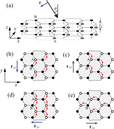
Phenomena in silicene in a strong optical pulse field are illustrated in Figs. 1(b)-(e). A strong optical field causes electron transfer in the direction of the force Schiffrin et al. (2012); Kelardeh et al. (2015). In fact, a strong optical field in the -direction (normal to the silicene plane) decreases symmetry of the system from honeycomb (six-order, centrosymmetric) to triangular (third-order, non-centrosymmetric). This leads to appearance of effects such as optical rectification and induction of currents normal to the in-plane component of the applied electric field.
Microscopically, the component of the strong field causes transfer of electrons between the sublattices. Assume for certainty that, for the chosen pulse, electrons are transferred from A to B. (Note that the change of the maximum field to the opposite, i.e., change of the carrier-envelope phase of the pulse by , would obviously cause an opposite transfer.) In the case of in-plane field polarized in the -direction, there is an electron transfer in both the - and -directions – see Fig. 1(b). The symmetry of the system dictates that with the reversal of (for the same -component, ) the -current changes to the opposite but the -current does not change, as shown in Fig. 1(c). This implies, in particular, that the system causes optical rectification in the -direction, which is due to the absence of symmetry with respect to the reflection in -plane for either sublattices.
Fundamentally different scenario takes place for in the direction – see Figs. 1(d) and (e). In this case, there is no current in the -direction due to symmetry with respect to reflection in the -plane. With respect to field changing to the opposite, the -current does not have any definite parity, which is rectification in the -direction.
To provide for the field-effect control of optical phenomena in silicene, the -component of the pulse electric field should be strong enough: , where is the optical frequency. Then, necessarily, the pulse should be very short, on the femtosecond scale, to allow the processes to be complete before significant damage to the lattice may have occurred – see Sec. II below. For such fields, there may be partial adiabaticity (reversibility) set on, which we will show below in Sec. III.
II Model and Main Equations
At the present time, record-setting ultrashort optical pulses have duration optical period Schiffrin et al. (2012); Schultze et al. (2012), with duration of just a few femtoseconds. We will idealize and simulate such an ultrashort pulse with the following single-oscillation waveform,
| (1) |
where is the amplitude, which is related to the pulse power, , is speed of light, , and is the pulse length, which is set fs. Note that this waveform has zero area, , which is required for a pulse propagating in far-field zone.
We consider a -polarized laser pulse with polarization direction parallel to the plane of incidence, orientation of which is determined by an angle measured relative to axis . Here the coordinate system is introduced in the plane of silicene/germanene, oriented as shown in Fig. 1(a). The angle of incidence of the laser pulse is denoted as .
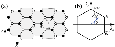
Similar to graphene, the silicene/germanene monolayer has honeycomb lattice structure, which is shown in Fig. 2(a). The lattice has two sublattices, labeled “A” and “B”, and is determined by two lattice vectors, and , where is lattice constant, which is Å for silicene and Å for germanene. The distance between the nearest neighbors is . The first Brillouin zone of the reciprocal lattice is a hexagon and is shown in Fig. 2(b). The points and are the Dirac points. In the buckled structure [see Fig. 1(a)], the -shift distance is Å and Å for silicene and germanene, respectively Liu et al. (2011d, e).
For a graphene monolayer, where spin-orbit coupling is extremely small ( meV), energy gaps at the Dirac points are correspondingly very small and can be set as zero for any practical purposes. Then the low energy spectra near the Dirac points are well described by the Dirac massless relativistic equation. For a silicene/germanene system, finite spin-orbit interaction opens up a much larger gap meV Ezawa (2012). Such a gap in the energy spectrum of silicene modifies low-energy electron transport and interaction between electrons in weak magnetic fields Apalkov and Chakraborty (2014). However, this spin-orbit interaction is too weak and, in our case, can be safely neglected compared to characteristic energy scale, , introduced by the strong electric field of the optical pulse in the buckled Dirac materials. At the same time, the buckled structure of a silicene monolayer introduces strong sensitivity of the system to the external normal field, Ezawa (2012). Hence, based on this consideration, below in this article we disregard the spin-orbit interaction but take into account the buckled structure bringing about the sensitivity to the normal optical electric field.
The Hamiltonian of an electron in silicene in the field of an optical pulse has the form
| (2) |
where is the field-free electron Hamiltonian, is a two dimensional vector, , and . Here the matrix form of the Hamiltonian corresponds to pseudo-spin, i.e., two components of the wave function and , which describe the amplitudes for an electron to be on the lattice site and , respectively.
The field-free electron Hamiltonian, , describes the nearest neighbor tight-binding model of silicene without spin-orbit terms. This Hamiltonian is exactly the same as the free-field Hamiltonian of graphene Wallace (1947); Slonczewski and Weiss (1958); Saito et al. (1998); Reich et al. (2004) and describes the tight-binding coupling between two sublattices A and B – see Fig. 2(a). In the reciprocal space, the Hamiltonian is a matrix of the form Wallace (1947); Slonczewski and Weiss (1958)
| (3) |
where the hopping integral is eV for silicene and for germanene Ezawa (2012), and
| (4) |
The energy spectrum of Hamiltonian consists of the conduction band (CB) (, or anti-bonding band) and the valence band (VB) (, or bonding band) with energy dispersion (CB) and (VB). The corresponding wave functions are
| (5) |
and
| (6) |
where .
The characteristic electron-electron scattering time in silicene/germanene is expected to be similar to the corresponding time is graphene, which is fs Hwang and Sarma (2008); Breusing et al. (2011); Malic et al. (2011); Brida et al. (2013); Gierz et al. (2013); Tomadin et al. (2013). The duration of the pulse in our problem ( fs) is . Therefore, it is not unreasonable to assume that the electron dynamics in the external electric field of the optical pulse is coherent and can be described by time-dependent Schrödinger equation
| (7) |
where Hamiltonian of Eq. (2) has an explicit time dependence.
The electric field of the optical pulse generates both interband and intraband electron dynamics. The interband dynamics introduces coupling of the states of the CB and VB and results in redistribution of electrons between the two bands. For dielectrics, such dynamics results in its metallization, which manifests itself as a finite charge transfer through dielectrics and finite CB population after the pulse ends Schiffrin et al. (2012); Krausz and Stockman (2014); Schultze et al. (2014).
In the reciprocal space, the intraband dynamics is described by the acceleration theorem Wannier (1960),
| (8) |
This acceleration theorem is universal and does not depend on the dispersion law. Therefore the intraband electron dynamics is the same for both the VB and CB. The time-dependent wave vector of an electron with initial wave vector can be found by solving Eq. (8) as
| (9) |
The corresponding electron wave functions are the well-known Houston functions Houston (1940),
| (10) |
where (VB) or (CB).
Using the Houston functions as a basis, we express the general solution of time-dependent Schrödinger equation (7) in the following form
| (11) |
Solution (11) is parametrized by initial electron wave vector . Due to the universal intraband electron dynamics in the reciprocal space, the equations, which describe coherent electron dynamics in the pulse field, become decoupled, greatly simplifying the problem.
Expansion coefficients satisfy the following system of differential equations
| (12) | |||
| (13) |
where function , which is given by the following expression,
| (14) |
is specific to the buckled structure of silicene. It determines the interband coupling induced by the perpendicular component of the pulse electric field. Vector function is proportional to the in-plane interband dipole matrix element,
| (15) |
where is the dipole matrix element between the states of the CB and VB with the same wave vector , namely,
| (16) |
Substituting Eqs. (5) and (6) into Eq. (16), we obtain explicitly,
| (17) |
and
| (18) |
System of equations (12)-(13) describes the interband electron dynamics and determines the mixing of CB and VB states in the electric field of the pulse. For undoped silicene, all VB states are initially occupied and all CB states are empty. Then the initial condition for system Eqs. (12)-(13) is , and the mixing of the states of different bands is characterized by time-dependent component . We also define the time-dependent total CB population by the following expression,
| (19) |
where the sum is over the first Brillouin zone. The CB population, , characterizes the electron dynamics in silicene and determines whether the dynamics for the entire system is reversible or not. Namely, the dynamics is reversible if, after the pulse ends, the CB population, which is the residual CB population, is small compared to the maximum CB population throughout the pulse.
Polarization of the system in a time-dependent electric field also generates electric current, which can be calculated in terms of the velocity operator from the following expression
| (20) |
where , and are matrix elements of the velocity operator . With the known wave functions (5)-(6) of the CB and VB, the matrix elements of the velocity operator are
| (21) | |||||
| (22) |
| (23) | |||||
and
| (24) |
The interband matrix elements of the velocity operator, and , are related to the interband dipole matrix elements, and Landau and Lifshitz (1965). Within the nearest-neighbor tight binding model, silicene has electron-hole symmetry, which results in the relation .
Let us denote current in the direction induced by in-plane field in the direction as , where . Similarly we denote charge transferred after the pulse ends through the system as . This is determined by an expression
| (25) |
The current can be expressed in terms of polarization of the electron system as . Then the transferred charge is determined by the residual polarization of the system as , where we introduced tensor indices for similarly to those for and . The transferred charge is nonzero only due to irreversibility of electron dynamics in the optical pulse field. For completely reversible dynamics, when the system returns to its initial state after the pulse, the transferred charge would be exactly zero.
III Results and Discussion
III.1 Band Population Dynamics in Strong Pulse Field
The principal distinction of silicene from graphene is that the sublattices, A and B, are separated “vertically” (i.e., in the -direction) by an appreciable distance, – see Fig. 1(a). The strong field of the optical pulse causes non-perturbative nonlinear changes in the material. Such phenomena are sensitive to the maximum field of the pulse, which is amplitude . For our choice of pulse Eq. (1), the maximum of the carrier oscillation occurs at the maximum of the pulse envelope, i.e., the carrier-envelope phase (CEP) is zero – see Fig. 3(a) illustrating the pulse waveform.
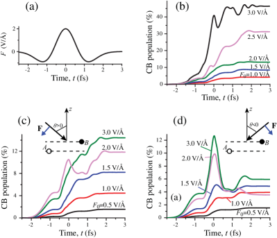
The CB population, , calculated in accord with Eq. (19) for pulse polarized in the plane is displayed in Fig. 3(b) as a function of time for different field amplitudes and incidence angle . Note that because silicene is symmetric with respect to reflection in the plane, the results for both and are identical. Two most prominent features of this dynamics are: (i) dependence on the pulse amplitude is very nonlinear, and (ii) the residual (after the pulse end) populations, are close to the maximum populations during the pulse. The latter property is similar to that in graphene Kelardeh et al. (2015). However, it is in a sharp contrast to that in silica, cf. Refs. Apalkov and Stockman (2012) (theory) and Schiffrin et al. (2012, 2014) (experiment) where the residual CB populations are relatively small. This large residual CB population for silicene suggests lack of adiabaticity, which is likely due to a relatively small distance of the transfer between the two sublattices in the plane, , in this case. Note that the adiabaticity parameter is . Adiabaticity requires while, in our case, even at the strongest fields, the adiabatic parameter is not too small, .
The response for the case of the pulse polarized in the plane is displayed in Figs. 3(c)-(d). In the stark contrast to the case of the polarization considered above in the previous paragraph, here there is a dramatic difference between and . This is due to the violation in the reflection symmetry induced by the component of the maximum field. For the case illustrated, this field promotes transfer of electrons predominantly toward the B sublattice – cf. Fig. 1(a).
For as shown in Fig. 3(c), the component of the maximum field, , promotes transfer of electrons from left to right (in the direction ) according to their negative charge – cf. Fig. 1(d). The distance of transfer is the same as in the case of the -polarized field and adiabaticity is violated since . Correspondingly, the residual CB populations are again close to their corresponding maxima during the pulse.
Dramatically different behavior takes place for the reciprocal incidence, where the CB population kinetics is displayed in Fig. 3(d). For relatively weak fields, , the kinetics is essentially irreversible, where the maximum CB population is attained at the end of the excitation pulse, similar to the case of Fig. 3(c) considered above in the previous paragraph. In a sharp contrast, for stronger fields, , there is partial reversibility: at the end of the pulse the CB population is reduced by a factor of with respect to its maximum. This is related to improved adiabaticity, i.e., decreased adiabaticity parameter, where is the horizontal transfer distance, see Fig. 2(a). This distance is twice longer than for the case of Figs. 1(c)-(d) corresponding to the polarizations in Figs. 3(b)-(c).
Note that the adiabaticity in the case of Fig. 3(d) is incomplete; for comparison, in the case of silica (quartz) a nearly perfect adiabaticity has been predicted and observed Apalkov and Stockman (2012); Schultze et al. (2012). This high degree of adiabaticity is most certainly related to a wide band gap, (see also Ref. Krausz and Stockman (2014)) and to a significantly larger lattice constant, , in quartz. Both these factors determine adiabaticity, which is pronounced when and . Thus one should not expect near-perfect adiabaticity in graphene (cf. Ref. Kelardeh et al. (2015)), silicene, and germanene where is negligible, and is relatively small.
III.2 Ultrafast Currents Induced by Strong Pulse
Electrical current is due to displacement of charges caused by the applied pulse field. For free classical electrons, this current is proportional to their mean velocity, i.e., to the integral of the field, often referred to as vector potential,
| (26) |
In contrast to free electrons, as we have argued above in Sec. III.1, the strong field acting on the electrons in crystal lattice of silicene causes effective symmetry reduction from honeycomb to triangular and, in particular, dependence of the electron dynamics on the sign of the maximum field – cf. Figs. 3 (c) and (d). The observed partial adiabaticity is also due to the presence of the periodic lattice and defined by its period in the field direction.
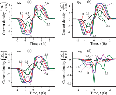
The effective reduction of symmetry to triangular (where there is no inversion center) caused by the strong normal () field component causes the currents in the silicene lattice to be highly anisotropic and non-reciprocal as we show below in this Section. Let us denote an -component of the current density induced by the field polarized in the plane with the maximum in the negative direction as shown in Fig. 3(c). Similarly, we denote the component of the current density caused by the field with the maximum in the positive direction as in the case of Fig. 3(d). Note that generally (as would have been the case for free electrons) due to the low, triangular effective symmetry.
Similarly, we introduce current density as the component of the current density induced by the polarized pulse. Note that in this case, the presence of the -symmetry plane dictates that . Interestingly enough, the in-plane field in the direction causes also a current in the direction [cf. Figs. 1 (b) and (c)], whose density we will denote as . Note that due to the symmetry, this current is invariant with respect to inversion in the plane, i.e., .
In Fig. 4, we plot the temporal behavior of the current density for the four independent cases of the pulse polarization and current direction, , , , and , as indicated in the panels; the currents in all other cases are either related to these cases by symmetry, as presented in the previous two paragraphs, or equal zero as, e.g., and . For the case shown in Fig. 4(a), in the relatively weak fields, , the current density, , obviously, qualitatively follows the vector potential, reaching (negative) maximum at approximately quarter oscillation period and turning to zero at the maximum field (). Kinetics is approximately antisymmetric with respect to point , which shows that this process is nearly time-reversible.
However, at higher fields, the behavior in Fig. 4(a) becomes nontrivial. The first manifestation of this behavior appears at where instead of a pronounced minimum (maximum negative current) there is a plateau, which turns to a maximum for . We attribute this behavior to electrons that are compelled by the field force to drift in the reciprocal space across the K-point. We will discuss this behavior in more detail in conjunction with Fig. 4(c) – see below.
A phenomenon of fundamental importance is the loss of adiabaticity in higher fields, which manifests itself in the lack of anti-symmetry with respect to point in Fig. 4(a). Note that non-adiabaticity also implies irreversibility 444Non-adiabaticity implies increase of entropy from the statistical or thermodynamic standpoint. Hence, non-adiabatic processes are irreversible. Examples of irreversible processes are seen in Fig. 3(b)-(c), while panel (d) shows partially reversible processes. and, consequently, violation of time-reversal symmetry (called also T-invariance or T-symmetry). This violation of adiabaticity is related to a gradual transfer of population between the A and B sublattices, as we discussed above in Sec. III.1. Such transfer is not instantaneous; one can estimate characteristic time it requires as . For a high field used, , we obtain . This is in a full qualitative agreement with the results of Fig. 4(a) where the time-reversal asymmetry becomes pronounced for high fields and times longer than from the moment the pulse is applied.
One of the consequences of the T-invariance violation are non-zero values of the transferred charge and of the residual polarization – see Eq. (25) and Fig. 6 and the corresponding discussion – violating the T-symmetry and adiabaticity. This implies that the system’s dynamics is irreversible (non-adiabatic), which may surprise one because the system is completely Hamiltonian. This is due to the fact that the central frequency of the laser radiation, , is close to the transition frequency between the electron states localized at the two sublattices, . This causes resonant absorption leading to dephasing – collisionless relaxation widely known as Landau damping Landau (1946).
Current kinetics for the case displayed in Fig. 4(b) is qualitatively similar to that for the case discussed above in the previous three paragraphs. However, the symmetry reduction caused by the nonlinear interaction with a controlled (zero in our case) CEP causes current to differ quantitatively from , which difference is pronounced in the second half-period () where the T-asymmetry of the current becomes evident. The latter is due to the non-adiabaticity, already mentioned above in the discussion of Fig. 4(a): the transfer of the electrons between sublattices occurs during a finite period of time, , comparable with half optical period in our case.
The case illustrated in Fig. 4(c) is not related by crystal symmetry or other invariances to the and cases considered above. However, the kinetics of is qualitatively similar to, though quantitatively different from, the previous two cases. Note that there is strict symmetry . Here also the T-symmetry is violated: the kinetics in the first and second half-periods is dramatically different. Note that in this case, current at the end of the pulse may not vanish, which is certainly due to absence of collisions and other interactions in the model. Note that the electron-electron collisions is the fastest interaction-induced relaxation process. However, it takes the electron-electron collisions in a similar two-dimensional system, graphene, to make an effect Brida et al. (2013), which is too long time for our pulse whose entire duration is less than 4 fs.
The results for current (in the direction induced by the field in the direction) are displayed in Fig. 4(d). Note that exactly due to symmetry. Without an electric field applied, silicene is a center-symmetric solid. Therefore for low fields current should vanish. This is, in fact, the case with a good accuracy for , as one can see in the Fig. 4(d). With field increasing, there is an increased current . Predominantly, it is directed along the negative axis, as is understandable from comparison with Figs. 1(b) and (c). Note that magnitude of this current is approximately an order of magnitude smaller than .
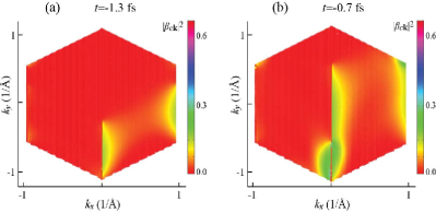
The origin of the current oscillations for strong fields, , in Figs. 4(a)-(c) can be understood from the electron momentum distribution. Consider for certainty the YY case, where the current is shown in Fig. 4(c). The corresponding momentum distribution for electrons in the CB, , for pulse field amplitude is displayed in in Fig. 5(a) for moment of time , corresponding to the minimum (the maximum negative value) of the current, . At this instance, which just precedes the current oscillation, excess electron population (depicted by green) is concentrated at , . This excess population is formed due to field force that pushes the electrons across the K points into the second Brillouin zone in the extended zone picture; these electrons appear in the first Brillouin zone at the K point at , . The second localization of electrons is around a K′ point at . This electron population is formed due to the lack of the center symmetry in the presence of strong field , i.e., it has the same origin at current described above in the previous paragraph.
Dramatically different electron distribution is displayed in Fig. 5(b) for when current experiences the maximum upswing. This is caused by a significant number of electrons in the CB with which appear due to a drift in the reciprocal space under force . These electrons make a positive contribution to the current (their group velocity ; correspondingly, due to , their contribution to is positive).
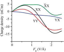
The currents described above in conjunction with Fig. 4 cause transfer of charge across the system and accumulation of charges by the end of the pulse as given by Eq. (25). Such charge transferred through the system is displayed as a function of the field amplitude, , in Fig. 6 for four independent combinations of the field and current directions, , , , and . A remarkable property of these results is that in all cases, except for , the charge transferred changes its sign as the field amplitude increases. This can be attributed to the increased number of electrons experiencing the Bragg reflections at the Brillouin zone boundary, especially at the K-points, with the field increase. Thus this sign change of the transferred charge has the same origin as the current oscillations in Fig. 4 as described above. This charge accumulated at the pulse end is an experimentally observable quantity just as the previous experiments on currents in dielectrics Schiffrin et al. (2012); Paasch-Colberg et al. (2014). On the order of magnitude, this accumulated charge in Fig. 6 is . For a focused spot, this gives a transferred charge. Such a charge is on the same order of magnitude as in experiments Refs. Schiffrin et al. (2012); Paasch-Colberg et al. (2014) and is, in principle, reliably observable.
IV Concluding Discussion
The accumulation of charge transferred through the system implies a dramatic manifestation of symmetry violation. This charge accumulation violates simultaneously the parity symmetry (P-symmetry) and the charge-inversion symmetry (C-symmetry). This violation happens due to the fact that our pulse is short and has a controlled CEP (zero in our case): the maximum field is reached at the maximum of the envelope (instance ). Due to strong nonlinearity of the system for fields applied, this maximum field defines a selected direction in the system plane for the force acting on electrons. This causes the violation of the C- and P-symmetries. This is actually a general property for systems subjected to a short, strong, CEP-controlled pulses. It takes place in both two-dimensional solids such as graphene, silicene, germanene, and also conventional three-dimensional solids such as fused silica, sapphire, etc. In particular, it was a fundamental origin for the charge transfer in silica and quartz in original experiments Schiffrin et al. (2012).
A symmetry violation specific for silicene is related to the electron transfer between the sublattices caused by the normal field component , which effectively reduces the system’s symmetry from hexagonal to triangular. This causes non-reciprocity: and the appearance of a cross-current, . Note that anisotropicity in the plane, , is inherent in both silicene and graphene.
Our zero-CEP pulse is T-symmetric; in the absence of the T-symmetry violation, the current should be T-odd, which would preclude the accumulation of charges after the pulse. However, we have seen from the results of Figs. 4(a)-(c) that the current is not anti-symmetric in time, i.e., there is a significant violation of the T-symmetry, which we attribute to the Landau damping. This is inherent in both graphene and silicene and is due to the absence of a significant band gap; this is in contrast to silica that is almost perfectly T-reversible Schiffrin et al. (2012); Schultze et al. (2012). An additional contribution to T-irreversibility stems from the fact that the frequency associated with the electron transfer in the normal direction, , is on the same order as the carrier frequency of the pulse. This causes resonant absorption of the excitation pulse and the Landau damping, specific for the silicene (and also germanene). If adiabaticity were present, it would have guaranteed reversibility and would have forbidden the charge accumulation.
Finally, we note a close analogy of silicene with the field-effect transistor (FET) Kahng (1963); Taur and Ning (1998); Liou and Schwierz (2003); Schwierz et al. (2010). In FET, the gate field, applied normally to the conducting channel, changes the carrier populations in it and, thereby, controls its conductance. Analogously, in silicene, the normal field component, , transfers carriers to one of the sublattices, A or B, thereby changing the system’s response to the in-plane field. A fundamental difference (and advantage) of silicene is that such a “device” works at optical frequencies, with the response time on the (sub)femtosecond scale. This opens a potential for many applications of silicene in future Petahertz-speed devices and applications.
Acknowledgment
The work of VA was supported by Grant No. ECCS-1308473 from NSF. This work of MIS and HKK was supported by major funding from from MURI Grant FA9550-15-1-0037 from the U.S. Air Force Office of Scientific Research; supplementary funding came from Grant No. DE-FG02-11ER46789 from the Materials Sciences and Engineering Division of the Office of the Basic Energy Sciences, Office of Science, U.S. Department of Energy and Grant No. DE-FG02-01ER15213 from the Chemical Sciences, Biosciences and Geosciences Division of the Office of the Basic Energy Sciences, Office of Science, U.S. Department of Energy.
References
- Kara et al. (2012) A. Kara, H. Enriquez, A. P. Seitsonen, L. C. Lew Yan Voon, S. Vizzini, B. Aufray, and H. Oughaddou, Surf. Sci. Rep. 67, 1 (2012).
- Tang and Zhou (2013) Q. Tang and Z. Zhou, Progr. Mater. Sci. 58, 1244 (2013).
- Rostami et al. (2013) H. Rostami, A. G. Moghaddam, and R. Asgari, Phys. Rev. B 88, 085440 (2013).
- Kormanyos et al. (2013) A. Kormanyos, V. Zolyomi, N. D. Drummond, P. Rakyta, G. Burkard, and V. I. Fal’ko, Phys. Rev. B 88, 045416 (2013).
- Takeda and Shiraishi (1994) K. Takeda and K. Shiraishi, Phys. Rev. B 50, 14916 (1994).
- Liu et al. (2011a) C.-C. Liu, W. Feng, and Y. Yao, Phys. Rev. Lett. 107, 076802 (2011a).
- Liu et al. (2011b) C.-C. Liu, H. Jiang, and Y. Yao, Phys. Rev. B 84, 195430 (2011b).
- Wang et al. (2012) Y. Wang, J. Zheng, Z. Ni, R. Fei, Q. Liu, R. Quhe, C. Xu, J. Zhou, Z. Gao, and J. Lu, Nano 07, 1250037 (2012).
- Zheng and Zhang (2012) F.-b. Zheng and C.-w. Zhang, Nanoscale Res. Lett. 7, 422 (2012).
- Lalmi et al. (2010) B. Lalmi, H. Oughaddou, H. Enriquez, A. Kara, S. Vizzini, B. Ealet, and B. Aufray, Appl. Phys. Lett. 97, 223109 (2010).
- De Padova et al. (2011) P. De Padova, C. Quaresima, B. Olivieri, P. Perfetti, and G. Le Lay, Appl. Phys. Lett. 98, 081909 (2011).
- Vogt et al. (2012) P. Vogt, P. De Padova, C. Quaresima, J. Avila, E. Frantzeskakis, M. C. Asensio, A. Resta, B. Ealet, and G. Le Lay, Phys. Rev. Lett. 108, 155501 (2012).
- Chen et al. (2012) L. Chen, C.-C. Liu, B. Feng, X. He, P. Cheng, Z. Ding, S. Meng, Y. Yao, and K. Wu, Phys. Rev. Lett. 109, 056804 (2012).
- Chun-Liang et al. (2012) L. Chun-Liang, A. Ryuichi, K. Kazuaki, T. Noriyuki, M. Emi, K. Yousoo, T. Noriaki, and K. Maki, Appl. Phys. Expr. 5, 045802 (2012).
- Feng et al. (2012) B. Feng, Z. Ding, S. Meng, Y. Yao, X. He, P. Cheng, L. Chen, and K. Wu, Nano Lett. 12, 3507 (2012).
- Fleurence et al. (2012) A. Fleurence, R. Friedlein, T. Ozaki, H. Kawai, Y. Wang, and Y. Yamada-Takamura, Phys. Rev. Lett. 108, 245501 (2012).
- Dávila et al. (2014) M. E. Dávila, L. Xian, S. Cahangirov, A. Rubio, and G. L. Lay, New J. Phys. 16, 095002 (2014).
- Li et al. (2014) L. Li, S.-z. Lu, J. Pan, Z. Qin, Y.-q. Wang, Y. Wang, G.-y. Cao, S. Du, and H.-J. Gao, Adv. Mat. 26, 4820 (2014).
- Tao et al. (2015) L. Tao, E. Cinquanta, D. Chiappe, C. Grazianetti, M. Fanciulli, M. Dubey, A. Molle, and D. Akinwande, Nat. Nano doi: 10.1038/nnano.2014.325 (2015).
- Kahng (1963) D. Kahng, United States Patent 3,102,230 (1963).
- Taur and Ning (1998) Y. Taur and T. H. Ning, Fundamentals of Modern VLSI Devices (Cambridge University Press, 1998).
- Liou and Schwierz (2003) J. J. Liou and F. Schwierz, Modern Microwave Transistors: Theory, Design and Performance (Wiley-Interscience, 2003).
- Schwierz et al. (2010) F. Schwierz, H. Wong, and J. J. Liou, Nanometer CMOS (Pan Stanford, 2010).
- Meng et al. (2013) L. Meng, Y. Wang, L. Zhang, S. Du, R. Wu, L. Li, Y. Zhang, G. Li, H. Zhou, W. A. Hofer, et al., Nano Lett. 13, 685 (2013).
- Liu et al. (2011c) C.-C. Liu, H. Jiang, and Y. Yao, Phys. Rev. B 84, 195430 (2011c).
- Gmitra et al. (2009) M. Gmitra, S. Konschuh, C. Ertler, C. Ambrosch-Draxl, and J. Fabian, Phys. Rev. B 80, 235431 (2009).
- Ezawa (2012) M. Ezawa, New J. Phys. 14, 033003 (2012).
- Schiffrin et al. (2012) A. Schiffrin, T. Paasch-Colberg, N. Karpowicz, V. Apalkov, D. Gerster, S. Muhlbrandt, M. Korbman, J. Reichert, M. Schultze, S. Holzner, et al., Nature 493, 70 (2012).
- Kelardeh et al. (2015) H. K. Kelardeh, V. Apalkov, and M. I. Stockman, Phys. Rev. B 91, 045439 (2015).
- Schultze et al. (2012) M. Schultze, E. M. Bothschafter, A. Sommer, S. Holzner, W. Schweinberger, M. Fiess, M. Hofstetter, R. Kienberger, V. Apalkov, V. S. Yakovlev, et al., Nature 493, 75 (2012).
- Liu et al. (2011d) C.-C. Liu, H. Jiang, and Y. Yao, Phys. Rev. B 84, 195430 (2011d).
- Liu et al. (2011e) C.-C. Liu, W. Feng, and Y. Yao, Phys. Rev. Lett. 107, 076802 (2011e).
- Apalkov and Chakraborty (2014) V. M. Apalkov and T. Chakraborty, Phys. Rev. B 90, 245108 (2014).
- Wallace (1947) P. R. Wallace, Phys. Rev. 71, 622 (1947).
- Slonczewski and Weiss (1958) J. C. Slonczewski and P. R. Weiss, Phys. Rev. 109, 272 (1958).
- Saito et al. (1998) R. Saito, G. Dresselhaus, and M. Dresselhaus, Physical Properties of Carbon Nanotubes (Imperial College Press, London, 1998).
- Reich et al. (2004) S. Reich, C. Thomsen, and J. Maultzsch, Carbon Nanotubes (Wiley-VCH, Weinheim, 2004).
- Hwang and Sarma (2008) E. H. Hwang and S. DasSarma, Phys. Rev. B 77, 195412 (2008).
- Breusing et al. (2011) M. Breusing, S. Kuehn, T. Winzer, E. Malic, F. Milde, N. Severin, J. P. Rabe, C. Ropers, A. Knorr, and T. Elsaesser, Phys. Rev. B 83, 153410 (2011).
- Malic et al. (2011) E. Malic, T. Winzer, E. Bobkin, and A. Knorr, Phys. Rev. B 84, 205406 (2011).
- Brida et al. (2013) D. Brida, A. Tomadin, C. Manzoni, Y. J. Kim, A. Lombardo, S. Milana, R. R. Nair, K. S. Novoselov, A. C. Ferrari, G. Cerullo, et al., Nat. Commun. 4 (2013).
- Gierz et al. (2013) I. Gierz, J. C. Petersen, M. Mitrano, C. Cacho, I. C. E. Turcu, E. Springate, A. Stöhr, A. Köhler, U. Starke, and A. Cavalleri, Nat. Mater. 12, 1119 (2013), ISSN 1476-1122.
- Tomadin et al. (2013) A. Tomadin, D. Brida, G. Cerullo, A. C. Ferrari, and M. Polini, Phys. Rev. B 88, 035430 (2013).
- Krausz and Stockman (2014) F. Krausz and M. I. Stockman, Nat. Phot. 8, 205 (2014).
- Schultze et al. (2014) M. Schultze, K. Ramasesha, C. D. Pemmaraju, S. A. Sato, D. Whitmore, A. Gandman, J. S. Prell, L. J. Borja, D. Prendergast, K. Yabana, et al., Science 346, 1348 (2014).
- Wannier (1960) G. H. Wannier, Phys. Rev. 117, 432 (1960).
- Houston (1940) W. V. Houston, Phys. Rev. 57, 184 (1940).
- Landau and Lifshitz (1965) L. D. Landau and E. M. Lifshitz, Quantum Mechanics: Non-Relativistic Theory (Pergamon Press, Oxford and New York, 1965).
- Apalkov and Stockman (2012) V. Apalkov and M. I. Stockman, Phys. Rev. B 86, 165118 (2012).
- Schiffrin et al. (2014) A. Schiffrin, T. Paasch-Colberg, N. Karpowicz, V. Apalkov, D. Gerster, S. Muhlbrandt, M. Korbman, J. Reichert, M. Schultze, S. Holzner, et al., Nature 507, 386 (2014).
- Landau (1946) L. D. Landau, Journal of Physics 10, 25 (1946).
- Paasch-Colberg et al. (2014) T. Paasch-Colberg, A. Schiffrin, N. Karpowicz, S. Kruchinin, S. Ozge, S. Keiber, O. Razskazovskaya, S. Muhlbrandt, A. Alnaser, M. Kubel, et al., Nat. Phot. 8, 214 (2014).