Electronic structure of interfaces between hexagonal and rhombohedral graphite
Abstract
An analysis of the electronic structure of interfaces between hexagonal (AB) and rhombohedral (ABC) graphite based on density functional theory is presented. Both of the two simplest interface structures host (localized) interface bands, which are located around the K-point in the Brillouin zone, and which give rise to strong peaks in the density of states at the Fermi level. All interface bands near the Fermi energy are localized at monomers (single atoms with dangling orbitals), whereas those around 0.5 eV belong to -bonded trimers, which are introduced by the interface and which are not found in the two adjacent bulk substances. There is also an interface band at the (AB) side of the interface which resembles one of the interface states near a stacking fault in (AB) graphite.
pacs:
73.21.Ac, 73.22.Pr, 73.20.At, 81.05.U-I Introduction
Stacking faults (SFs) in graphitic stacks play an important role for the electronic properties, because they induce localized bands and sharp peaks in the local density of states (LDOS) near the SFs and the Fermi energy . This is especially important because the two competing periodic bulk structures (hexagonal (AB) and rhombohedral (ABC) graphite) have a very small intrinsic density of states (DOS) at Taut et al. (2013, 2014). Therefore, the stacking faults produce virtually two-dimensional (2D) electron gases with little coupling to the bulk states and a thickness (extent) of a few lattice constants.
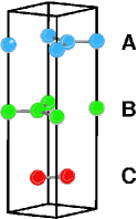
In a series of 3 papers we investigated the electronic structure of stacking faults, restricting ourselves to the simplest possibility where the SF separates two monolithic bulk blocks, as well as the cases of single displaced surface layers. In principle, there are 3 highly symmetric possibilities: both blocks can be hexagonal Taut et al. (2013), or rhombohedral Taut et al. (2014), or one block is hexagonal and the other one is rhombohedral (this paper). In each case there are two possibilities (denoted by and , depending on whether the shift between the two blocks is +1/3 or -1/3 of the lateral lattice constant. For displaced surface layers on hexagonal Taut et al. (2013) or rhombohedral Taut et al. (2014) graphite there is only one possibility in either case. The intriguing new feature in interfaces between hexagonal and rhombohedral graphite is that (semi)localized bands are possible which decay into one, or the other, or into both bulk materials.
For the one-particle spectra the generalized gradient approximation (GGA) Perdew et al. (1996) has been used, whereas total energies are calculated with the local density approximation (LDA). The reason for this choice has been discussed in detail in Taut et al. (2013). are compared with those from the LDA. The calculation of the electronic properties was done with the Full-Potential Local-Orbital DFT package (FPLO) fpl ; Koepernik and Eschrig (1999); Opahle et al. (1999) using default settings except for the -mesh of the Brillouin zone (BZ) integration, which is specified at the appropriate places in the text below.
II Projected bulk band structure
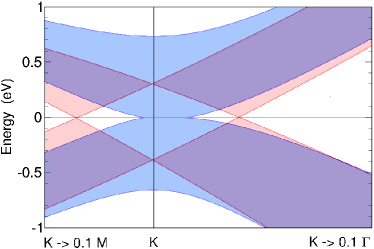
The projected bulk band structure (PBBS) is a very helpful device for the interpretation of calculations of the electronic band structure of interfaces. It consists of broad quasi-continuous bands which comprise the electronic bands with periodic boundary conditions as a function of for quasi-continuous as parameters, where are the Cartesian coordinates parallel to the interface and is perpendicular to it. The bulk band structures of and graphite can be found in Refs.Taut et al. (2013) and Taut et al. (2014), respectively, and the PBBSs around the K-point are shown in Fig.2 as shades of different color in the same plot. Evanescent states for each and can exist in each material only in gaps of the corresponding PBBS Heine (1963, 1964), because in the bulk state continuum an evanescent state could mix with a bulk state (of the same energy and and ) and thus turn into a bulk state or interface resonance.
Fig.2 shows the regions where states can exist which fall off into the (AB) bulk, into the (ABC) bulk, and into both sides. Obviously, at the very K point only boundary states which fall off into the (ABC) bulk are allowed, but there are windows on both symmetry lines (K-M and K-) near the K point where real localized states can occur. We have to consider, however, that this rule is exactly valid only for interfaces of two infinite (or sufficiently thick) blocks of different materials. In case of any doubt one has to analyze the character of the wave functions, e.g. by calculating the band weights (see Ref.Taut et al. (2013)).
III Types of Interfaces
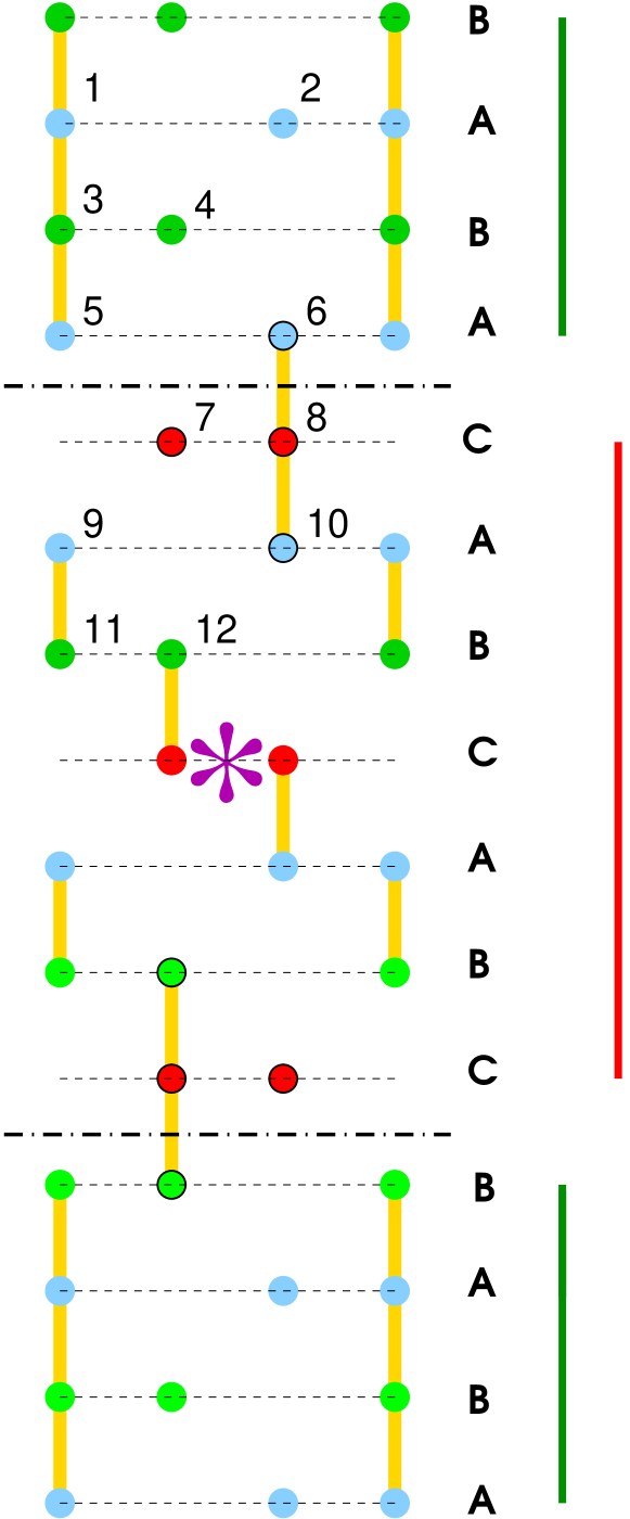
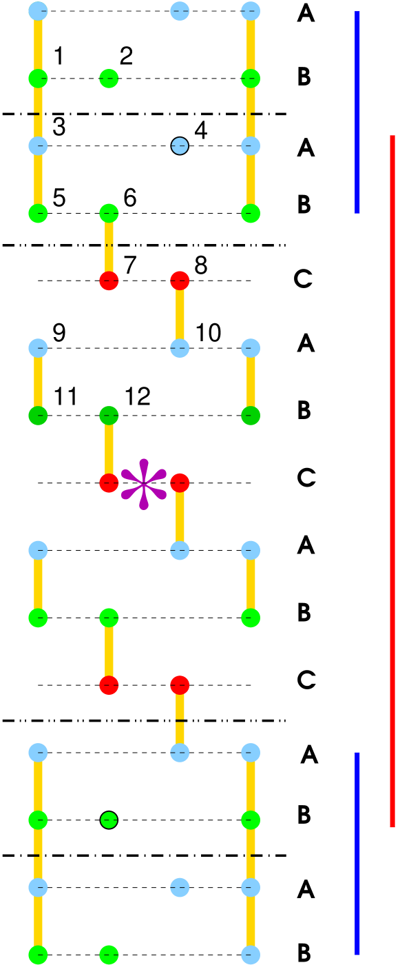
For our calculations of interfaces we used a super-cell geometry, for which the unit cell is chosen such that two interfaces per unit cell and an inversion center in the middle are obtained (see Fig.3). The inversion symmetry reduces the numerical effort considerably and prevents the formation of dipole moments. Another possible option are slabs with one interface in the middle, which are periodically repeated and separated by finite layers of vacuum. In this case an inversion center (or a mirror plane) cannot be accommodated, but the electronic structure of the surface could be studied together with the interface. Because the surfaces have been investigated already in the former works Taut et al. (2013) and Taut et al. (2014), we preferred the super-cell model in this work, and use the slab model only for double-checking. For establishing an inversion center, we added an additional C-layer on top of the (ABC) block. This trick makes the (ABC) block just one layer thicker, but does not disturb the stacking order. Please note, that the unit cells shown in the figure are just for visualization and the real calculations are done with much thicker unit cells as described in the figure caption.
As in our previous investigations of stacking faults, there are two types
of simple interfaces, which are denoted by and and which
differ in their local bonding picture and consequently
also in their electronic properties (see Fig.3).
Interfaces in graphite stacks can create interface clusters, which
are not present in the adjacent bulk blocks.
(A monomer is considered here as a special case of a cluster, and the term
’monomer’ and ’single atom’ are considered as synonyms.)
In type the periodicity is broken at
a plane which can be located
between atoms 5,6 and 7,8 (restricting ourselves to the upper half of the cell).
Consequently, the
trimer (atoms 6, 8, and 10)
and an additional monomer outside the (AB) block (atom 7) do not belong to
the adjacent bulk structures and should be considered as interface clusters.
In type , the matter is not that easy.
If we approach the interface:
(i) from the side of the (AB) block, the periodicity
is broken at the plane between atoms 5,6 and 7,8, and atom 4 would
be part of the (AB) block and therefore no interface cluster.
(ii) Alternatively, from the (ABC) side, the periodicity
is broken at the plane between atoms 3,4 and 1,2 and atom 4 does not belong
to the (AB) block and consequently it should be
an interface monomer.
Consequently, in this case
this issue cannot be decided on the basis of simple geometry.
As we will see in the Section III.B, atom 4 hosts an interface state
with the same characteristics as the
interface state at atom 7 in type ,
and therefore atom 4 in type should be considered as an interface monomer.
III.1 Interface
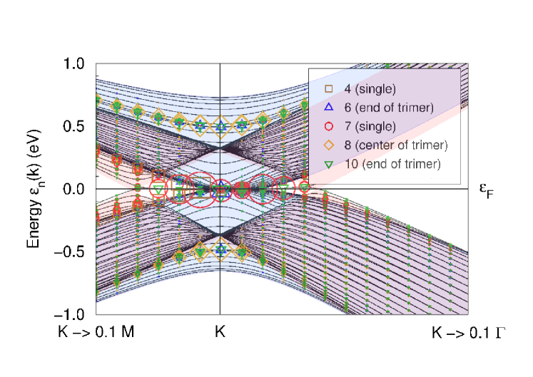
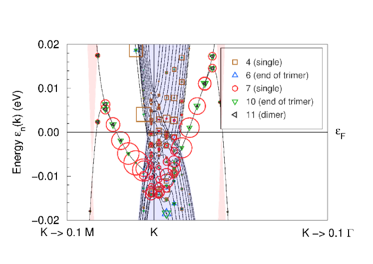
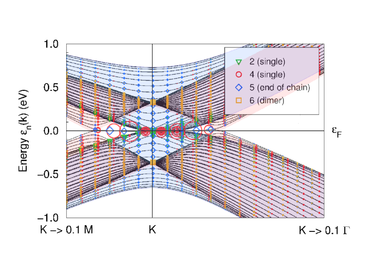
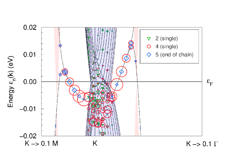
Fig. 4 shows the bands around the Fermi level including band weights (for definition see Introduction of Ref.Taut et al., 2013) for certain atomic positions and along the symmetry line M-K- in the basal plane around the K-point. Because the Brillouin zone of the super-cell is about 65 times wider than high, the dispersion in direction is practically not visible and therefore not shown. Note, that in infinite super-cells all interface bands would be doubly degenerate due to the occurance of two interfaces per unit cell. In our finite super-cells, however, these bands can split up, upon approaching the bulk state continuum, because then the decay length converges to infinity and the interface states of the two interfaces overlap. This effect is clearly seen in the lower panel of Fig. 4 and Fig. 7, where the interface bands approaches the (red) bulk band continuum of (ABC) graphite.
As in the previous papers on stacking faults in (AB) and (ABC) graphite, some of the interface bands at the K point can be understood qualitatively using a simple model for the interface clusters. In this model the atoms of the clusters are bound to each other only by one effective overlap integral =0.345 eV perpendicular to the layers (see Appendix in Ref. Taut et al., 2014). The reason why the interface clusters are virtually decoupled from the adjacent bulks is that at the K point the coupling between atoms in the same layer cancels, and the interface clusters have no nearest neighbors in adjacent bulk layers (see e.g. Ref. Guinea et al., 2006). In our case, this model provides a monomer state at E=0, and for the trimer one state at E=0 with eigenvector and a pair of states at E= with eigenvectors . The first eigenstate is located only at end-atoms of the trimers, whereas the pair of states has its main weight in the center.
(i) The most prominent interface band related to an interface cluster is near the Fermi level and is mainly localized at the monomers (No.7, red circles) at the interface (see Fig. 4, lower panel). In the window outside of both bulk continua, its wave function decays into both adjacent bulk blocks, whereas upon approaching the (ABC) continuum it hybidizes mainly with the end atom of the trimer No.10 and dimer atom No.11 (not the much closer atom No.9 !) and correspondingly the band weight of atom No.7 decreases.
(ii) A pair of interface bands is localized at the trimer (atoms No. 8, 6 and 10, blue and green triangles and golden diamonds) with energies around 0.5 eV. Closer examination of the weights of further atoms than those shown in Fig. 4 reveals that these trimer bands are localized in both directions perpendicular to the interface, despite the fact that they are located within the (AB) bulk continuum. Hybridization of interface and bulk states, which share the same region in the E - space may take place, but can be suppressed or reduced in certain symmetry or binding configurations.
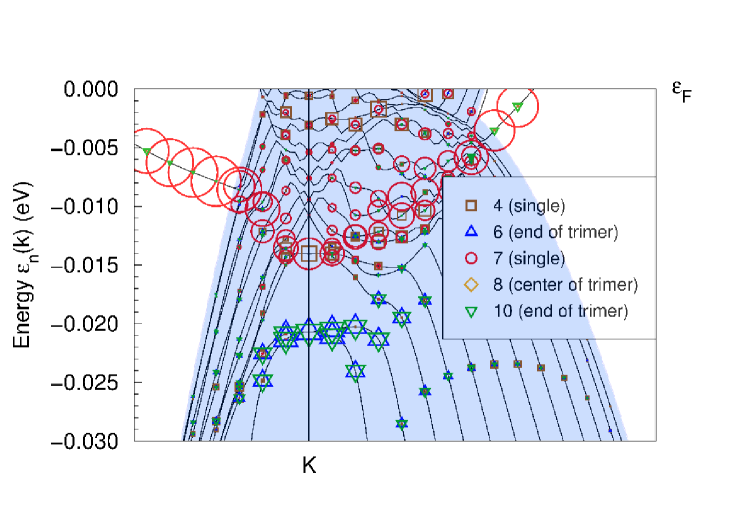
(iii) The third trimer state with energy at the K-point around -0.02 eV is visible in the special zoom shown in Fig.5. Its wave function is located at the ends of the trimer (atoms No. 6 and 10, blue and green triangles). Like the pair of trimer bands discussed in (ii), it is localized in both directions perpendicular to the interface.
There is a different type of interface band, however, which is localized at the monomer No.4 (brown squares), which is not an interface cluster, but it is the monomer within the (AB) bulk structure closest to the interface. The dispersion of this band differs completely from the interface-cluster-induced bands. Therefore we call it surface-band-like. This interface band runs close and almost parallel to the boundary of the (AB) bulk continuum and it resembles the interface bands near a stacking fault in (AB) graphite reported in Ref. Taut et al., 2013. Note, that this band is not restricted to positive energies as it seems in the lower panel of Fig. 4. Only in the energy window between -0.02 and 0 it is suppressed by the strong interface band located at atom No.7 (red circles). Closer examination of the upper panel reveals that it reappears in the energy range below -0.02. However, this band is strictly localized only on the line K 0.1 M (left of the (AB) continuum), but on K 0.1 it lies within the continuum and turns into an interface resonance.
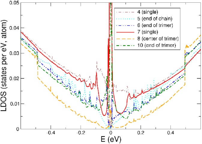
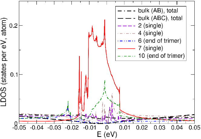
In Fig. 6 the LDOS is presented for a selection of atoms on two different energy scales. The most prominent peak at the Fermi energy comes from the interface band at the monomer (single atom No.7). The next larger contribution to the LDOS at the Fermi energy is located at one end of the trimer (atom No.10) and stems from the low-energy trimer band. The high-energy trimer bands (at atoms 6, 8, and 10) around 0.5 eV, which have a 2D dispersion of type , produce only the steps in the LDOS seen in the upper panel.
III.2 Interface
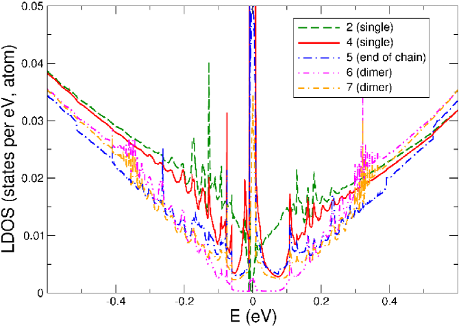
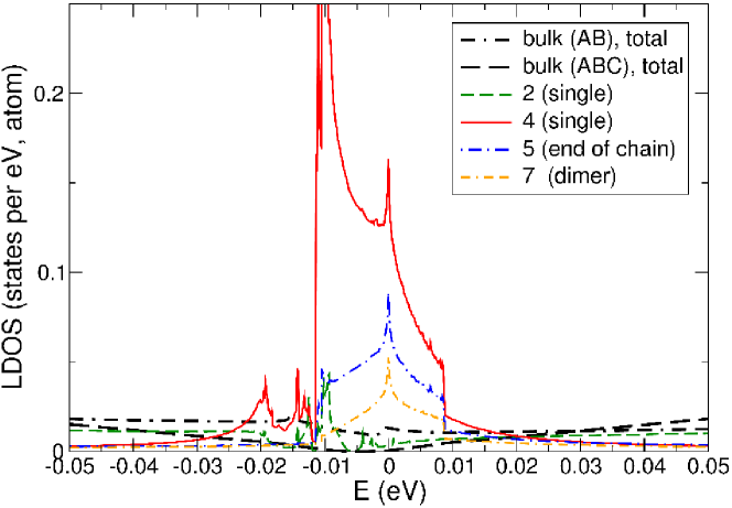
The bands in slab shown in Fig. 7 are less rich in interface bands because there is only one monomer which can be considered as an interface cluster. The corresponding interface band is located at atom 4 and its dispersion is very similar to the band located at atom 7 in type . Correspondingly, the LDOS at the Fermi energy shown in Fig. 8 is dominated by the peak from this band. Smaller peaks are from atoms 5 and 7. The contribution of atom 6 (not shown) is much smaller than the contribution of the atoms included in the figure, even though it is located close to the interface as well and belongs to the same dimer. The latter effect is similar to that in type , where the contribution of atom 9 is much smaller than atom 11. In type we do not have a surface-band-like interface band which is the equivalent of the band at atom 4 in , i.e., a band which is located at the monomer within (but close to the border of) the (AB) bulk block. This shows that the surface-band-like interface bands are very sensitive to details of the structure, as well known from non-topological surface bands.
IV Interface energy
The interface energy per interface atom is defined in analogy to formula (7) in Ref. Taut et al. (2013)
| (1) |
where is the total energy of the super-cell with atoms, and and are the total energies per atom for hexagonal and rhombohedral bulk graphite. The factor considers the fact that we have two interfaces per unit cell and two atoms in each interface layer. Unlike in the case of stacking faults, however, we cannot subtract in (1) the ground state energy of the supercell without interface, because this definition would lead to a quantity which is roughly proportional to the distance of the interfaces. Instead we subtract the total energy of a fictitious system, in which the two bulks extend upto the mathematical interface plane. This provides a quantity which is (in the limit of thick supercells) independent of thickness. Note, however, that is not the formation energy of the interface, but it can be used to find the most probable interface structure. As seen in Table 1, structure is energetically much more favourable than . Comparison with the data on hexagonal graphitic stacks given in Ref. Taut et al. (2013) shows that the interface energy between hexagonal and rhombohedral graphite presented here is one order of magnitude larger than stacking fault energies, but one to two orders smaller than surface energies. On the other hand, the energy differences given in Table 1 are of the same order as the difference in the total energies (per atom) of bulk hexagonal and rhombohedral graphite given in Ref. Taut et al. (2013) as well.
| system | formula | |
|---|---|---|
| 257.1 | ||
| 64.2 |
V Summary
A central role for the interpretation of interface bands is played by interface clusters. They are caused by the interface and do not exist in the adjacent bulk materials. In this series of papers we met monomers, dimers, linear trimers, and linear tetamers. Monomers and trimers host interface bands around the Fermi energy, and dimers, trimers and tetramers also at finite energies in the range between 0.2 and 0.5 eV. (Please note, that monomers and dimers can also belong to the bulk blocks of (AB) and (ABC) graphite, respectively. In this case they are not called ’interface clusters’.)
In this paper we investigated the two simplest
types of interfaces between hexagonal (AB)
and rhombohedral (ABC) graphite: type hosts two different
interface clusters, namely trimers and monomers, whereas
type has only interface monomers.
From total energy calculations it follows that
type has the lower interface energy and it is therefore
more probable to occur.
Both interfaces produce interface bands near the K point in the Brillouin zone.
These interface bands can be categorized into two two groups:
(i) Most of the interface bands can be traced back to interface clusters.
In type , they are localized at atom 7 (monomer) and atoms 6, 8, and 10 (trimer),
and in type at atom 4.
(ii) However, there is also the possibility
for surface-band-like interface bands,
which are localized at the border, but within the adjacent bulk materials.
In type , the band localized at atom 4 (which belongs to the (AB) block)
is such a case.
As in the case of non-topological surface states, the existence
of the second type of interface bands depends
on the details of the structure and potential near the surface/interface.
Interface hosts none of this type.
Interface bands near the Fermi energy produce large peaks in the LDOS, which in turn should lead to large contributions to the local conductivity along the interfaces. The trimer bands around eV cause only steps in the LDOS.
Acknowledgements.
We are indebted to M. Richter for support and helpful discussions.References
- Taut et al. (2013) M. Taut, K. Koepernik, and M. Richter, Phys. Rev. B 88, 205411 (2013).
- Taut et al. (2014) M. Taut, K. Koepernik, and M. Richter, cond-ma-1014303t (2014).
- Lipson and Stokes (1942) H. Lipson and A. R. Stokes, Proc. R. Soc. A 181, 101 (1942).
- Perdew et al. (1996) J. Perdew, K. Burke, and M. Ernzerhof, Phys. Rev. Lett. 77, 3 865 (1996).
- (5) http://www.fplo.de/, version: 9.01-35-x86_64.
- Koepernik and Eschrig (1999) K. Koepernik and H. Eschrig, Phys. Rev. B 59, 1743 (1999).
- Opahle et al. (1999) I. Opahle, K. Koepernik, and H. Eschrig, Phys. Rev. B 60, 14035 (1999).
- Heine (1963) V. Heine, Proc. Phys. Soc. 81, 300 (1963).
- Heine (1964) V. Heine, Surf. Sci. 2, 1 (1964).
- Guinea et al. (2006) F. Guinea, A. H. C. Neto, and N. M. R. Peres, Phys. Rev. B 73, 245426 (2006).