Spontaneous Appearance of Low-dimensional Magnetic Electron System on Semiconductor Nanostructures
Abstract
We find that spin-polarized ground states emerge in nanofacets which are self-organized on SiC (0001) surfaces. Our large-scale density-functional calculations reveal that the nanofacet formed by bunching of single bilayer steps generates peculiar carbon dangling bond states localized at but extended along step edges. The flat-band characteristics of those C states cause either ferromagnetic or anti-ferromagnetic chains on covalent semiconductors.
pacs:
73.20.-r, 75.70.Rf, 71.20.Nr, 61.46.-wNanometer-scale structures are now accessible through cutting-edge fabrication technique itrs or a gift of self-organization phenomena shchukin ; rousset ; giesen ; eaglesham ; hirayama . Common expectation that such nanostructures break through limitations of current technology may rely on a fact that nano-scale shapes affect wave-functions of relevant electron states. However, a way of designing nano-shapes which decisively affect the electron states and therefore are intriguing in science and useful in technology is lacking.
One of the unexpected but promising examples is the spin-polarization or the magnetism in nanostructures of covalent semiconductors, that is occasionally called magnetism akiyama ; uchida ; gohda ; vankatesan . Particular arrangements of unpaired electrons on hydrogen-covered Si (111) surface okada1 and on Au-covered high-Miller index Si surface erwin1 ; erwin2 are predicted to be ferrimagnetic and anti-ferromagnetic (AFM), respectively, by the density-functional calculations. The spin-polarization on the Si surface is indeed evidenced by photoemissionbierdermann ; yeom and scanning tunneling microscopeaulbach experiments.
However, such nanostructures are achieved only by sophisticated fabrication techniques on semiconductor surfaces. It would be free from such difficulty if the self-organization could produce desirable nanostructures by itself. We here report occurrence of magnetic chains on self-organized nanostructures of silicon carbide (SiC).
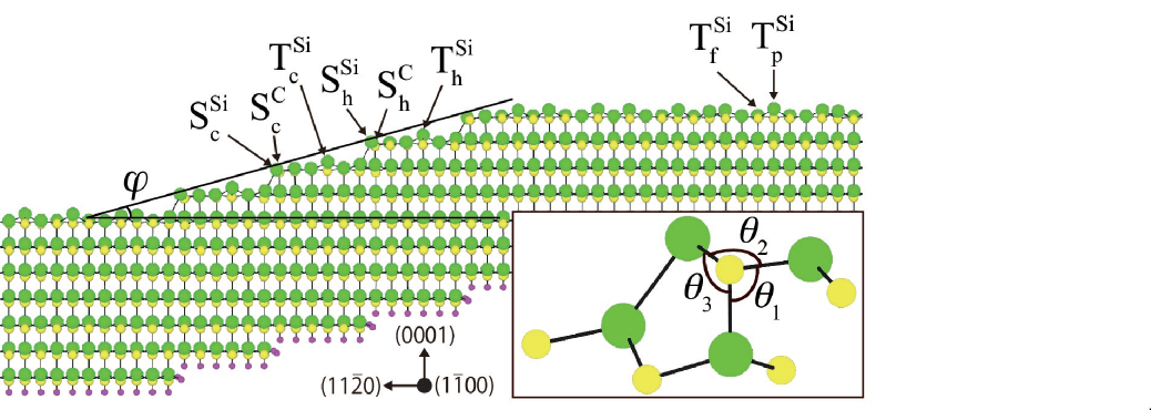
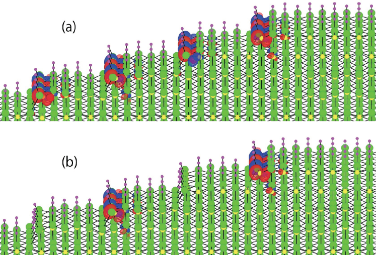
SiC is a wide gap covalent semiconductor, existing as many polytypes such as 2H (wurtzite), 3C (zincblende), 4H, 6H and so forth polytype . The 4H is the most stable with larger cohesive energy than others by 0.2 meV per SiC unit. Due to its high dielectric breakdown voltage and the high melting temperatureSiC , SiC is a strong candidate for the next-generation devices in environment-friendly power electronicsSiC ; rabkowski . This material shows peculiar nanostructures through self-organization: During the epitaxial growth of SiC (0001) surface, the (11) nanofacets are frequently observed nakamura ; nakagawa ; fujii (Fig. 1); the facet angle which is the angle between (0001) and (11) is almost the same (magic angle, = 12∘ - 16∘) and the height of the nanofacet along the (0001) direction is a integer or a half-integer of the unit-cell heightnakagawa ; fujii ; kimoto ; arima ; nie . The mechanism of such nanofacet formation is clarified by our recent density-functional calculations sawada : Microscopically, the nanofacet is the bunched single bilayer atomic steps; the balance between the step-step repulsive energy and the surface-energy gain on the terrace is the reason for the formation of the particular nanofacet structure, strongly indicative of that such nanaofacet is ubiquitous on semiconductor surfaces.
In this Letter, we show that peculiar electron states which are localized near but extended along step edges of the nanofacets of SiC exhibit either ferromagnetic (FM) or AFM spin polarization. Based on the density-functional calculations, we find that hydrogen passivation of the surface spontaneously induce such spin polarization.
Most calculations have been performed by the local density approximation (LDA) kohn ; lda in the density functional theory (DFT) hohenberg ; kohn . Key results are crosschecked by the generalized gradient approximation (GGA) gga to the exchange-correlation energy functional. We use our own real-space code named RSDFT iwata1 ; iwata2 ; hasegawa combined with the norm-conserving pseudo-potentials TM . We have examined effects of core corrections pcc on the magnetic states and found that they are unimportant in the system of C and Si. The real-space scheme is most suitable to current multi-core massively parallel architecture and allows us to perform extensive calculations for thousands-atom systems. Details are given in Supplementary Material SM .
We have performed extensive total energy calculations for the (11) nanofacet structures of 4H-SiC SM and obtained the most stable structure with the facet angle being 15.3∘ sawada , in accord with the experiments nakagawa ; fujii ; kimoto ; arima ; nie . The structure is a nano-aggregate of bunched single bilayer steps, as shown in Fig. 1 and Supplementary Figure 1 (SFig. 1) SM . The bilayer atomic stacking is ABCBABCB from the topmost surface.
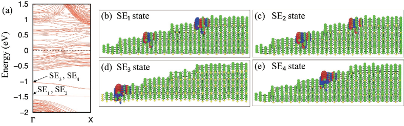
Let us start with the calculated electronic structure of this nanofacet (Fig. 2). Near the Fermi level (), we observe many states which have characters of dangling bonds (DBs) of surface Si atoms on the long terrace. The energy bands more than 1.5 eV below is mainly ascribed to the valence bands of the bulk SiC, whereas the bands at about 1 eV above are from the bulk conduction bands. Apart from those states, we have found four distinct states in the energy gap, labeled as SE1, SE2, SE3 and SE4 in Fig. 2(a). From the analyses of the Kohn-Sham (KS) orbitals of these states [Figs. 2 (b)-(e) and Fig. 3], we have found that they originate from the step-edge states: The KS orbitals of the SE1 and SE2 states are localized near the step edges where the upper terraces have cubic symmetry (i.e., the stacking sequence from the top is either ABC or CBA; cub-terrace edge hereafter), whereas the orbitals of SE3 and SE4 states are near the step edges where the upper terraces have the hexagonal symmetry (i.e. the stacking sequence is either BCB or BAB; hex-terrace edge hereafter). They are localized near but extended along the step edges, exhibiting dispersion-free flat bands.
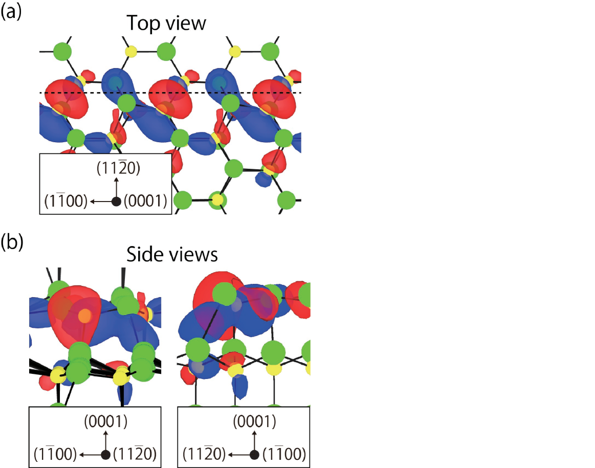
Figure 3 clearly shows that those step-edge states have the character of the dangling bonds (DBs) of the three-fold coordinated edge C atoms. They are also mixed with the back-bond character of neighboring edge Si atoms. The states which have the character of DBs of the edge Si atoms are located around , being substantially resonant with the terrace DB states. Larger electron affinity of C than Si renders the DB-character state of C to be located at lower energy positions being distinct from the Si DB-character states.
| terrace | cub | cub | hex | hex | ||
|---|---|---|---|---|---|---|
| (o) | 98.9 | 99.3 | 96.1 | 96.3 | ||
| (o) | 126.8 | 127.5 | 129.8 | 130.5 | ||
| (o) | 101.4 | 101.7 | 108.7 | 108.6 |
The splitting between the SE1 and SE2 group and the SE3 and SE4 group comes from structural characteristics of the step edges. Table 1 shows the bond angles, , , and , at the step-edge C atom. We have found small but sizable difference in the bond angles between cub-terrace edge and hex-terrace edge C atoms. Applying the -orbital axis vector analysis (POAV) hyb to the three-fold coordinated C atoms where the three bonds are formed by hybridization and the remaining DB has a character of orbital, we can deduce the amount of hybridization and from the bond angles, , , and hyb . The obtained values for the amounts of characters in the DBs are and for the cub-terrace edge C and and for the hex-terrace edge C. The larger mixing with -character renders the SE1 and SE2 states lower than SE3 and SE4 states by a half eV.
| site | T | T | T | T | S | S | S | S | ||
|---|---|---|---|---|---|---|---|---|---|---|
| 1.71 | 1.68 | 1.67 | 1.65 | 1.56 | 1.34 | 1.33 | 1.25 |
Figure 2 unequivocally show the existence of flat bands on semiconductor nanofacets. The flat band may generally causes ferromagnetism lieb ; mielke ; tasaki , and its manifestation in graphene is reported fujita ; okada2 . We now find that hydrogen passivation realizes the possibility of flat-band magnetism on the SiC nanofacet. It is of note that the H-passivation on semiconductor surfaces is an extremely common and useful fabrication technique tsuchida ; sieber ; seyller . Table 2 shows the calculated H-adsorption energies adsorption for various atomic sites on the nanofacet. It is found that depends on the adsorption site. First, the H adsorption with the Si atoms is favorable energetically compared with the C atoms. As stated above, the orbital energy of the Si dangling bond (DB) is higher due to its smaller electron affinity. Before H passivation, some of Si DBs are doubly occupied and others are empty. The H passivation of Si DBs generates doubly occupied Si-H bonding states, thus leading to the larger H adsorption energy. Second, the H adsorption with the edge atoms is less favorable compared with the terrace atoms. This is due to the relaxation around the step edges: As represented in Table 1, the edge DBs have more component in their characters, leading to lower orbital energies and less energy gain upon the H passivation. The adsorption energy of the Si atom on the hex-terrace edge (S) is relatively large. This is due to the attractive electrostatic interaction between Si and C in the 4H structure edgeSi .
Calculated difference in H-adsorption energies in Table 2 indicates that the terrace Si atoms are easily terminated by the H adsorption, whereas the edge atoms are likely to survive with their DBs. The Si atom at the hex-terrace edge is an exception with its large adsorption energy explained above. Hence, when we set an energy criterion of 0.2 eV, it is plausible that the surface atoms are passivated by H except for the edge C atoms and the Si atoms at the cub-terrace edge. This situation is possible by control of temperature.
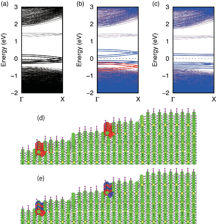
Figure 4 shows energy bands and spin densities of such H-passivated nanofacet. We have found that shifts downward and crosses the flat bands passivation . Then we have obtained three solutions of KS equation: The non-magnetic (NM), FM and AFM states. The total energy of the AFM state is the lowest, being followed by the FM state with the energy increase of 19 meV (7.9 meV) per spin and then the NM state with further increase of 83 meV (225 meV) in our LDA (GGA) calculations. In the NM state, crosses the energy bands with the DB character of the hex-terrace edge C atoms (states SE3 and SE4). The character of Si DBs at the edge is absent in these bands due to the electron affinity difference so that the dispersion along the edge becomes smaller than expected from the atomic arrangement. Hence the exchange plus correlation splitting in the KS orbitals of the C DBs is 0.78 eV and 0.72 eV in the FM and AFM states, respectively, leading to the spin-polarized state in the SiC nanafacet. The AFM state in preference to the FM state which we have found is provisionally ascribed to the prominent flat-band nature in the AFM state induced by the localization of the edge carbon DB (CDB) state. However, it is plausible that the AFM and FM states coexist in suitable temperature range. It is of note that the spin density [Figs. 4 (d) and (e)] is solely distributed along the hex-terrace edges, reflecting atom-scale reconstruction near edges explained above.
The situation we have explained is characterized as the spin-polarization in the three-quarter filling flat bands. The filling by electrons is controlled by the H-passivation. When all the edge atoms are free from the H-passivation, which may be possible by increasing temperature, we have a situation that all CDB states are occupied and Si DB states are unoccupied, leading to the semiconducting character (not shown here). When all the Si edge atoms as well as the terrace Si atoms are passivated, the CDB states are half-occupied. We have found the AFM and FM states in this case in the range of the total energy of 9.9 meV. The NM state is higher in energy by 100 meV. The spin density in the AFM state is shown in Fig. 5 (a). Interestingly, the spin density is now distributed to all the edges including the cub-terrace edges. This is caused by the filling control of the CDB states by the H passivation. When the C atoms at the cub-terrace edge, which produce the least adsorption energy, is free from the H passivation, we encounter a situation in which a CDB state at the cube-terrace edge is half filled. We have found the FM and AFM states in the range of 0.1 meV per spin, being lower than the NM state by 141 meV. In this case, the spin density is distributed solely along the cub-terrace edges[Fig. 5(b)].
In summary, we have performed large-scale density-functional calculations on the stable 4H-SiC nanofacet and found that the spin polarization along the step edges in the nanofacet emerges. This comes from the localization of the electron states caused by the electron affinity difference between C and Si and by the peculiar atomic structures of SiC surface. We have found that the hydrogen passivation is a powerful tool to control the spin polarization in the system with ubiquitous elements of H, C and Si.
Acknowledgements.
This work was supported by the Grants-in-Aid for scientific research under Contract No. 22104005 and also by “Computational Materials Science Initiative”, both conducted by MEXT, Japan. Computations were performed mainly at K Computer in Advanced Institute for Computational Science, RIKEN and at Supercomputer Center in ISSP, University of Tokyo.References
- (1) International Technolgy RoadMap for Semiconductors: http://www.itrs.net/
- (2) A. Shchukin and D. Bimberg, Rev. Mod. Phys. 71, 1125 (1999).
- (3) S. Rousset, F. Pourmir, J. M. Berroir, J. Klein, J. Lecoeur, P. Hecquet, and B. Salanon, Surf. Sci. 422, 33 (1999).
- (4) M. Giesen and T. L. Einstein, Surf. Sci. 449, 191 (2000).
- (5) D. J. Eaglesham, F. C. Unterwald, and D. C. Jacobson, Phys. Rev. Lett. 70, 966 (1993).
- (6) H. Hirayama, M. Hiroi, and T. Ide, Phys. Rev. B 48, 17331 (1993).
- (7) T. Akiyama and A. Oshiyama, J. Phys. Soc. Jpn. 70, 1627 (2001).
- (8) K. Uchida, And A. Oshiyama, J. Phys. Soc. Jpn. 79, 093711 (2010).
- (9) Y. Gohda and A. Oshiyama, Phys. Rev. B78, 161201(R), (2008).
- (10) M. Venkatesan, C. B. Fitzgerald, J. M. D. Coey, Nature 430, 630 (2004).
- (11) S. Okada, K. Shiraishi, and A. Oshiyama, Phys. Rev. Lett. 90, 026803 (2003).
- (12) S. C. Erwin and F. J. Himpsel, Nat. Commun. 1, 58 (2010).
- (13) S. C. Erwin and P. C. Snijders, Phys. Rev. B 87, 235316 (2013).
- (14) K. Biedermann, S. Regensburger, Th. Fauster, F. J. Himpsel, and S. C. Erwin, Phys. Rev. B 85, 245413 (2012).
- (15) H. W. Yeom, S. W. Jung, J. S. Shin, J. Kim, K. S. Kim, K. Miyamoto, T. Okuda, H. Namatame, A. Kimura, and M. Taniguchi, New J. Phys. 16, 093030 (2014).
- (16) J. Aulbach, J. Schfer, S. C. Erwin, S. Meyer, C. Loho, J. Settelein, and R. Claessen, Phys. Rev. Lett. 111, 137203 (2013).
- (17) In tetrahedrally bonded semiconductors, there are possible polytypes in which the stacking of atomic bilayers along the bond direction is different. Each polytype is labeled by the periodicity of the stacking sequence and the symmetry (cubic or hexagonal) such as 2H (wurtzite), 3C (zincblende), 4H, and 6H. The sequence of the most stable 4H polytype is ABCB where A, B and C denote 3 possible ways of the stacking.
- (18) Silicon Carbide edited by P. Friedrichs, T. Kimoto, L. Ley, and G. Pensl, vol. 1 - 2. (Wiley-VCH, Weinheim, 2010).
- (19) J. Rabkowski, D. Peftitsis, and H.-P. Nee, IEEE Industrial Electroncis Magazine, 6, 17 (2012).
- (20) S. Nakamura, T. Kimoto, H. Matsunami, S. Tanaka, N. Tearguchi, and A. Suzuki, Appl. Phys. Lett. 76, 3412 (2000).
- (21) H. Nakagawa, S. Tanaka, and I. Suemune, Phys. Rev. Lett. 91, 226107 (2003)
- (22) M. Fujii and S. Tanaka, Phys. Rev. Lett. 99, 016102 (2007).
- (23) T. Kimoto, A. Itoh, and H. Matsunami, Appl. Phys. Lett. 66, 3645 (1995).
- (24) K. Arima, H. Hara, J. Murata, T. Ishida, R. Okamoto, K. Yagi, Y. Sano, H. Mimura, and K. Yamauchi, Appl. Phys. Lett. 90, 202106 (2007).
- (25) S. Nie et al., Surf. Sci. 602, 2936 (2008).
- (26) K. Sawada, J. -I. Iwata and A. Oshiyama, Appl. Phys. Lett. 104, 051605 (2014).
- (27) W. Kohn and L. J. Sham, Phys. Rev. 140, A1133 (1965).
- (28) J. P. Perdew and A. Zunger, Phys. Rev. B 23, 5048 (1981).
- (29) P. Hohenberg and W. Kohn, Phys. Rev. 136, B864 (1964).
- (30) J. P. Perdew, K. Burke, and M. Ernzerhof, Phys. Rev. Lett. 77, 3865 (1996); 78, 1396 (1997).
- (31) S. G. Louie, S. Froyen, and M. L. Cohen, Phys. Rev. B 26, 1738 (1982).
- (32) J. -I. Iwata, K. Shiraishi, and A. Oshiyama, Phys. Rev. B 77, 115208 (2008).
- (33) J. -I. Iwata, D. Takahashi, A. Oshiyama, B. Boku, K. Shiraishi, S. Okada, and K. Yabana, J. Comput. Phys. 229, 2339 (2010).
- (34) Y. Hasegawa, J.-I. Iwata, M. Tsuji, D. Takahashi, A. Oshiyama, K. Minami, T. Boku, H. Inoue, Y. Kitazawa, I. Miyoshi, M. Yokokawa, International Journal High Performance Computing Applications, 28, 335-355 (2014).
- (35) N. Troullier and J. L. Martins, Phys. Rev. B 43, 1993 (1991).
- (36) See Supplementary Material http://xxx for details of the calculations.
- (37) R. C. Haddon, J. Am. Chem. Soc. 108, 2837 (1986).
- (38) E. H. Lieb, Phys. Rev. Lett. 62, 1201 (1989); 62, 1927 (1989).
- (39) A. Mielke, J. Phys. A 24, L73 (1991); 24, 3311 (1991); 25, 4335 (1992).
- (40) H. Tasaki, Phys. Rev. Lett. 69, 1608 (1992); Prog. Theor. Phys. 99, 489 (1998).
- (41) M. Fujita, K. Wakabayashi, K. Nakada, and K. Kusakabe, J. Phys. Soc. Jpn 65, 1920 (1996).
- (42) S. Okada and A. Oshiyama, Phys. Rev. Lett. 87, 146803 (2001).
- (43) H. Tsuchida, I. Kamata, and K. Izumi, Jpn. J. Appl. Phys. 36, L699 (1997).
- (44) N. Sieber, B. F. Mantel, Th. Seyller, J. Ristein1, L. Ley, T. Heller, D. R. Batchelor, and D. Schmeier, Appl. Phys. Lett. 78,1216 (2001).
- (45) T. Seyller, J. Phys. Condens. Matter 16, S1755 (2004).
- (46) The H-adsorption energy is defined as with and being the total energies of the nanofacet without and with, respectively, H atoms. The is the chemical potential of H atoms and is regarded here as a half of an energy of an H2 molecule.
- (47) Due to the difference in electronegativity, the electron transfer from Si to C takes place in SiC. At the site S, the third-nearest-neighbor C atom in the subsurface is located with the short distance of 2.86Å. This leads to the electrostatic energy gain upon H adsorption which causes positively charged Si edge atom.
- (48) Hydrogen passivation of Si annihilates Si DB states, which are either unoccupied or doubly occupied, and induces H-Si bonding and anti-bonding states, thus shifting downwards.