Generation of photovoltage in graphene on a femtosecond time scale through efficient carrier heating
Abstract
Graphene is a promising material for ultrafast and broadband photodetection. Earlier studies addressed the general operation of graphene-based photo-thermoelectric devices, and the switching speed, which is limited by the charge carrier cooling time, on the order of picoseconds. However, the generation of the photovoltage could occur at a much faster time scale, as it is associated with the carrier heating time. Here, we measure the photovoltage generation time and find it to be faster than 50 femtoseconds. As a proof-of-principle application of this ultrafast photodetector, we use graphene to directly measure, electrically, the pulse duration of a sub-50 femtosecond laser pulse. The observation that carrier heating is ultrafast suggests that energy from absorbed photons can be efficiently transferred to carrier heat. To study this, we examine the spectral response and find a constant spectral responsivity between 500 and 1500 nm. This is consistent with efficient electron heating. These results are promising for ultrafast femtosecond and broadband photodetector applications.
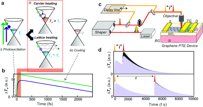
Photovoltage generation through the photo-thermoelectric (PTE) effect occurs when light is focused at the interface of monolayer and bilayer graphene, or at the interface between regions of graphene with different Fermi energies Wei2009 ; Xu2010 ; Song2011 ; Gabor2011 ; Freitag2013 ; Koppens2014 . In such graphene PTE devices – which operate over a large spectral range Bonaccorso2010 ; Echtermeyer2014 that extends even into the far-infrared Cai2014 – local heating of electrons by absorbed light, in combination with a difference in Seebeck coefficients between the two regions, gives rise to a photo-thermoelectric voltage . Here and are the Seebeck coefficients of regions 1 and 2, respectively, is the hot electron temperature after photoexcitation and electron heating, and the temperature of the electrode heat sinks. The performance of PTE graphene devices is intimately connected to the dynamics of the photoexcited electrons and holes, which have mainly been studied in graphene samples through ultrafast optical pump-probe measurements George2008 ; Breusing2011 ; Gierz2013 ; Tielrooij2013 ; Johannsen2013 ; Lui2010 ; Jensen2014 ; Brida2013 . As shown in Fig. 1a, the dynamics start with i) photo-excitation and electron-hole pair generation; followed by ii) electron heating through carrier-carrier scattering, in competition with lattice heating, which both take place on a sub-100 fs time scale; and finally iii) electron cooling by thermal equilibration with the lattice, which takes place on a picosecond time scale. The effect of the picosecond cooling step iii) on the switching speed of graphene devices has been studied using time-resolved photovoltage scanning experiments with 200 fs time resolution Sun2012 ; Urich2011 ; Graham2013 . These studies showed that the picosecond electron cooling time limits the intrinsic photo-switching rate of these devices to a few hundred GHz, because faster switching would reduce the switching contrast, as the system does not have time to return to the ground state. Indeed, GHz switching speeds have been demonstrated in graphene-based devices Gan2013 ; Xia2009 ; Schall2014 ; Mueller2010 ; Pospischil2013 .
However, the most crucial aspects of the photo-thermoelectric response are captured by the heating dynamics, as electron heating corresponds to photovoltage generation. Additionally, these dynamics determine the ultimate intrinsic carrier heating efficiency and the resulting spectral response. Here, we measure the photovoltage generation time with an unprecedented time resolution, and assess its effect on the heating efficiency through spectral responsivity measurements. In an ideal photo-thermoelectric detector, all the absorbed photon energy is transferred rapidly to electron heat (before energy is lost through other channels). In this case, doubling the photon energy would lead to doubling of the photovoltage (see Fig. 1b), and would result in a flat spectral responsivity , where is the generated photocurrent and is the excitation power. In strong contrast, the spectral response of conventional semiconductor-based detectors is not flat at all, since it is determined by the band gap: Photons with an energy below the band gap are not absorbed, i.e. = 0, and the excess energy above the band gap typically does not lead to an additional photoresponse, i.e. a decreasing with photon energy Sze .
Photovoltage generation on a femtosecond time scale
In order to capture the time scale of photovoltage generation, we perform time-resolved photovoltage measurements with the highest time resolution to date of 30 fs. We achieve this by using a broadband Ti:Sapphire 85 MHz oscillator (center frequency 800 nm, bandwidth 100 nm) that creates 20 fs pulses, and a pulse shaper that corrects for any dispersion (and thus pulse stretching) that the pulses pick up on their way from the laser to the device (see Fig. 1c and Supp. Info for details). The concept of the experiment is illustrated in Fig. 1d. We use a pair of ultrashort laser pulses, where the two pulses are separated by a controllable delay time and focused onto a single spot on the device. The two pulses contain different spectral components to suppress coherent artifacts. We then record the photocurrent, averaged over a large number of pulse pairs, as a function of delay . After absorption of the first pulse, the electron temperature rises by , and then starts cooling down to . If the second pulse arrives before reaches (i.e. when the delay between the two pulses is shorter than the cooling time), the electron temperature rises again but by less than . This is because the electronic heat capacity of a degenerate electron gas increases with electron temperature Kittel and , with the heat in the system before photoexcitation and the absorbed power from a laser pulse. Thus, the additional amount of generated photovoltage by the second pulse is lower than when the pulses would each contribute independently. As a result, the photovoltage as a function of delay time directly reflects the time dynamics of the electron temperature and therefore also the PTE induced photovoltage.
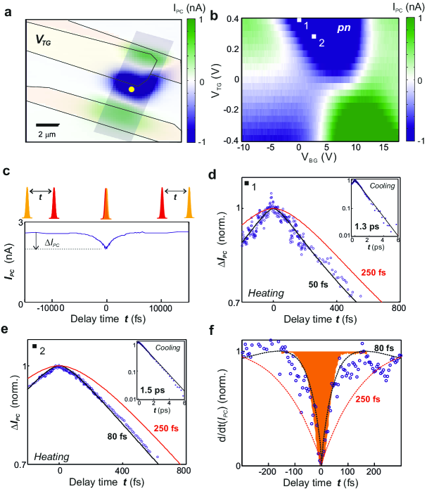
We apply our femtosecond photovoltage sensing technique to a graphene -junction device, that consists of a bottom and top dual-gated graphene flake (“dual-gated device”, see Supp. Info). A scanning photocurrent image is shown in Fig. 2a, where the top gate and bottom gate voltages are such that a -junction is formed at the edge of the top gate. Figure 2b shows the photocurrent with the laser focused at this position, as a function of back-gate and top-gate voltages. The multiple sign reversals indicate that the photovoltage is generated through the PTE effect Song2011 ; Gabor2011 . We show the photocurrent generated in this device as a function of in Fig. 2c, which clearly shows a dip around . In Fig. 2d-e, we show the normalized photocurrent dip for two combinations of gate voltages, both in the -regime. The decays on both sides of reflect the cooling dynamics with a picosecond time scale, as observed in Refs. Sun2012 ; Urich2011 ; Graham2013 . Around we notice that the photocurrent dip is remarkably sharp, which is only possible when the time resolution of the complete system (i.e. the laser pulses and the graphene photoresponse) is sufficiently high. Any decrease of time resolution, either because of longer pulses or due to a slower generation of the photovoltage in graphene, would lead to a broadening of the apex of the inverted v-shape.
We use two approaches to quantitatively determine the time scale of photovoltage creation. In the first approach, we characterize the sharpness of the photocurrent dip around by taking the time-derivative. In the Supp. Info we show that in the case of exponential heating dynamics, taking the derivative directly recovers the heat dynamics: , where and are the electron heating and electron cooling time scales, respectively. Figure 2f shows the experimentally obtained together with the heating dynamics using 80 fs, obtained from a best fit. To show that we can indeed resolve time scales shorter than the time scale that was accessible in earlier time-resolved studies Graham2013 ; Sun2012 ; Urich2011 , we also plot the dynamics with fs. This slower heating time clearly does not fit the experimental data. In the second approach we develop a model for the photovoltage as a function of , based on heating dynamics induced by the pulse-pair excitation and including nonlinear heating (see Methods). We show the data for the first (second) gate voltage combination in Fig. 2d(e), together with the modeled photocurrent change . We find excellent agreement between data and model for 50 (80) fs and a cooling time of 1.3 (1.5) ps. As an illustration we show the model for fs, which is clearly in strong disagreement with the data. We thus conclude that for the -junction configuration, photovoltage generation occurs within 50 fs.
We now put this capability of ultrafast photovoltage generation into the perspective of an application. The switching speed of graphene optoelectronic devices using the direct photoresponse is limited by the picosecond cooling time, as shown by earlier reports Xia2009 ; Urich2011 , and limited to a few hundred GHz. However, we envision femtosecond photosensing applications by exploiting the nonlinear heating response and combining graphene PTE devices with time-differential operation. Here, we provide one proof-of-principle demonstration: we use the graphene photodetector to measure in a direct electrical signal the duration of an ultrashort femtosecond laser pulse. We compare the derivative photocurrent signal with the optical cross correlation signal that is measured by overlapping the two laser pulses in a second harmonic generation crystal and monitoring the second harmonic signal at 400 nm as a function of delay time (orange area in Fig. 2f). The agreement shows that our graphene PTE device is capable of measuring the pulse width of the laser down to time scales below 50 fs, in a direct electrical signal, and without the use of non-linear crystals. We note that this technique will work over a much broader spectral range (from the ultraviolet Tielrooij2013 to the terahertz Cai2014 ) than techniques based on two-photon absorption in silicon photodiodes or frequency conversion in nonlinear crystals, and has a similar sensitivity.
Efficient photo-induced carrier heating
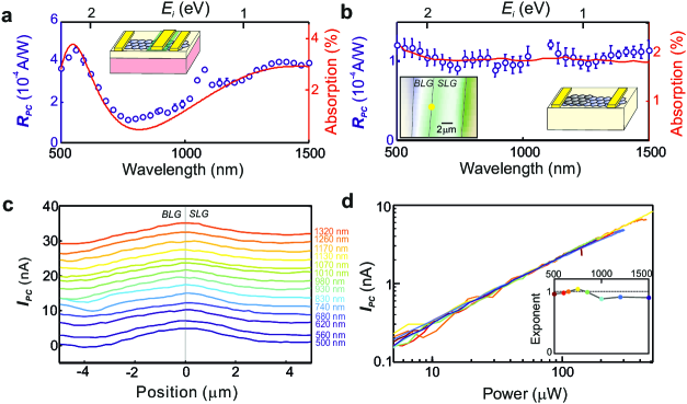
Having established that carrier heating and PTE photovoltage generation occur on a femtosecond time scale, we now address how this step affects the energy conversion efficiency of graphene PTE devices. The main question is if the carrier heating is fast enough to out-compete energy loss processes, such as optical phonon emission (step ii) in Fig. 1a). To this end, we study the photoresponse for a wide range of photon energies, from 0.8 (1500 nm) to 2.5 eV (500 nm). We use a laser source (quasi-CW (continuous wave), since the pulse duration of 20 ps is larger than the cooling time of 1 ps) with a controllable wavelength and a constant excitation power . In Fig. 3a, we show the (external) responsivity for the dual-gated -junction device. This spectral response is dominated by the strongly wavelength-dependent absorption spectrum of the device, which is the result of reflections at the oxide-silicon interface and the sub-wavelength oxide thickness (see Supp. Info). This effect is very similar to the enhanced reflection for certain combinations of wavelength and oxide thickness, which enhance the contrast of graphene in an optical microscope Blake2007 . Indeed, the calculated graphene absorption (using Lumerical FDTD Solutions software) agrees well with the wavelength-dependent responsivity.
To avoid the strongly wavelength-dependent absorption, we use a graphene device that is supported by a transparent substrate that consists of 1 mm thick quartz (“transparent substrate device”, see Supp. Info). The flake contains both single- and bilayer graphene, with PTE photovoltage generation at the interface Xu2010 . Figure 3b shows the responsivity spectrum at the monolayer-bilayer interface, together with the measured graphene absorption on a similar device. These data are obtained from spatially resolved measurements (Fig. 3c), which show that the spatial extent of the photoresponse does not change with wavelength. The spectral response (for constant excitation power) of the device is strikingly constant over this broad range of excitation wavelengths. The flat shows that decreasing the number of incident photons (by increasing the photon energy) does not lead to a decrease in photovoltage: thus a higher photon energy gives a larger photovoltage, as in Fig. 1b. This is in stark contrast with photovoltaic detectors based on semiconductors, where the photovoltage generally decreases for increasing photon energy, meaning that excess energy is lost Sze . The flat at the monolayer-bilayer interface is therefore consistent with photo-thermoelectric current generation (which also applies to the graphene-metal interface; see Supp. Info).
To understand the flat, broadband for constant absorbed power, we examine what this result means for the electron heating as a function of photon energy. First we note that the photovoltage scales linearly with power for all wavelengths (see Fig. 3d), which means that we are in the “weak heating” regime where and the electronic heat capacity is constant (in contrast to the “strong heating” regime in the ultrafast experiment, where the scaling is sublinear). The reason for the small heating is that we use more than 10 times lower power and quasi-CW laser excitation with 20 ps laser pulses, which is longer than the cooling time of 1 ps (leading to a peak power that is 3 orders of magnitude smaller than for ultrafast excitation). In this “weak heating” regime, the cooling rate is constant Graham2013 , which means that the conversion efficiency is not affected by the life time of the hot electrons. Furthermore, the Seebeck factor does not change with excitation wavelength. Therefore, from the flat we conclude that the light-induced increase in electron temperature at constant power is the same for all photon energies.
This result enables us to assess the efficiency of the electron heating (in the “weak heating” regime). We examine two alternative ultrafast energy relaxation pathways for photo-excited electrons and holes: carrier-carrier scattering and optical phonon emission (see Fig. 1a). Graphene optical phonons have an energy of 0.2 eV and therefore photoexcited carriers above 0.2 eV can in principle relax by emitting a phonon. The faster process of these two competing processes will dominate the ultrafast energy relaxation. We have determined the time scale of carrier-carrier scattering (through the photovoltage generation in the “dual-gated device”) to be 50 fs. The time scale of phonon emission is typically 150 fs Breusing2011 ; Lui2010 , and therefore this does not give a definite answer about which ultrafast relaxation process dominates. However, from the measured spectral responsivity we can extract the heating efficiency.
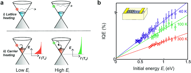
We illustrate this by considering two contrasting cases (see Fig. 4a): i) dominant coupling of photo-excited electrons to optical phonons, with a small fraction of the absorbed photon energy converted into hot electrons and ii) dominant carrier-carrier scattering Winzer2010 ; SongPRB2013 with a large fraction of the energy converted into hot electrons. In case i, the energy loss rate through optical phonon emission increases linearly with initial electron energy , since it is governed by a constant electron-phonon coupling, and an energy-momentum scattering phase space that increases linearly with energy Tielrooij2013 (see Fig. 4a). Thus in case i, a larger leads to more energy loss to phonons. On the other hand, in case ii, the electron temperature scales linearly with , because the energy of the photoexcited electron is fully transferred to the electron gas. Thus, the role of optical phonon emission can be measured by studying the scaling of with . This relationship, extracted from the photovoltage measurements, is shown in Fig. 4b, where we plot the internal quantum efficiency (IQE = ). The IQE represents the generated photovoltage, normalized by the number of absorbed photons. We find (nearly perfect) linear scaling of the IQE with , as the linear fits go nearly trough the origin. This means that a higher photon energy corresponds to a larger photovoltage and thus to a larger , which is consistent with terahertz photoconductivity measurements SongPRB2013 ; Tielrooij2013 ; Jensen2014 , where a terahertz probe provided a measurement of the carrier temperature. We therefore conclude that the generated photovoltage comes from ultrafast, efficient photon-to-electron-heat conversion and an unmeasurably small loss to optical phonons.
To show that carrier heating is indeed efficient, we calculate the expected temperature rise and use the measured photovoltage to determine the Seebeck factor , which we then compare to its expected value. Details are given in the Methods section. To calculate we use a simple heat equation and assume fully efficient carrier heating to find 0.17 K ( 50 W, 300 K, 250 meV, 1 ps). We then use the measured photovoltage of 10 V, where is the device resistance (2 k). We conclude that 65 V/K. This is very close to the maximum expected value using a charge puddle width of 80 meV, which gives 90 V/K. Having confirmed that carrier heating is efficient, we aim to gain insight into the other factors that determine the overall energy conversion efficiency of the device. One important factor is the hot carrier lifetime, which should be long (low cooling rate) to lead to a larger photovoltage. We verify this by changing the ambient temperature. First we demonstrate that the efficiency of electron heating is independent of lattice temperature, as we obtain the same linear scaling through the origin for a lattice temperature of 40, 100 and 300 K. We then note that the overall photovoltage is larger for lower lattice temperatures. This is caused by the longer cooling time at low temperatures, due to a lower coupling between electrons and acoustic phonons Graham2013 ; Ma2014 ; Song2011 . The Seebeck coefficient decreases with temperature, meaning that the overall generated photovoltage is about a factor two larger Graham2013 .
Conclusion
The unique femtosecond time resolution and the related high carrier heating efficiency are very encouraging results for bias-free (passive) PTE photodetectors. To improve the internal quantum efficiency of 1% (Fig. 4b), an interesting approach (see Methods for details) would be to use ultraclean, defect-free graphene, such as in Ref. Wang2013 , which enables detector operation with a higher Seebeck coefficient, because the electron-hole puddle density is lower (see Methods). The small puddle width could increase the Seebeck factor to 300 V/K. Measuring at 50 meV instead of 250 meV would furthermore lead to a larger , since this scales with (due to the lower heat capacity upon approaching the Dirac point). With 50 W excitation a of almost 1 K is feasible (assuming an unmodified carrier cooling rate), giving V. A resistance of 1 k Wang2013 would then give an IQE of 100% or more. Our results thus show that graphene PTE devices exhibit ultrafast, efficient and broadband photodetection. Future photodetection and light harvesting devices could exploit these graphene properties and combine them with the advantageous properties of other 2D materials. Future work could investigate the effect of the Fermi energy on the heating time, the time-resolved signal generation in devices based on the bolometric effect Freitag13b ; Yan2012 , and the effect of the substrate on the heat dynamics.
Methods
Simulation of the photocurrent dynamics
Here we describe how we extract the hot electron dynamics from the photocurrent dip . This analysis draws on the procedure described in Ref. Graham2013 . We start with a laser-induced change in electron temperature for single pulse excitation assuming a linear response: . Here is the ’real’ time, the electron heating time and the electron cooling time. We then introduce a nonlinearity (any type of nonlinearity works) of the form (with the lattice temperature) and calculate the integrated photovoltage generated by two pulses well separated in time (adding up independently): . We now follow the same procedure for two-pulse excitation where the pulses arrive with a separation of delay time and obtain (linear response) and
(with nonlinearity). This temperature change is shown in Fig. 1d of the main text in ’real’ time for two different delay times . We use these electron temperature dynamics to calculate the integrated voltage , and repeat this for a range of delay times . The photocurrent dip as a function of delay time is then given by . This dip grows upon approaching , but flattens when . The reason for this is that when the two pulses arrive at exactly the same time (), there is no heating yet due to any of the two pulses and they independently start leading to electron heating and thus contributing to the photovoltage. As a result, the photocurrent dip flattens around . We note that the dip should not disappear, since we measure the time-integrated photocurrent and once the electrons start heating up, the heating induced by the two pulses is no longer independent. Finally, we point out that all dynamics are determined by the local (at the junction) carrier heating and PTE voltage creation. All dynamics that happen after this (propagation of the potential to the contacts, signals traveling through the cables, etc.) do no affect the results of our specific experiment. To measure transit times, one can use two-pulse excitation with two different focus spots Son2014 .
Calculation of , and
We calculate the theoretical and experimental photovoltage in the case of excitation with 50 W of light (of which 2 % is absorbed, See Fig. 3b), in the case of the “transparent substrate device”, where the photovoltage is created at the interface of monolayer and bilayer graphene, at room temperature. We calculate the temperature increase from a simple heat equation (in the case of a cooling length that is smaller than the spot size) to be Freitag2013 :
| (1) |
Here, the laser focus spot size is 1.5 m (see Fig. 3c), and the cooling rate is given by , where , with , and the reduced Planck constant, the Fermi velocity and Boltzmann’s constant, respectively. We use 0.25 eV and a cooling time of 1 ps, which we obtained from ultrafast photocurrent measurements on the same device. This yields a cooling rate of 0.4 MW/m2K, close to theoretical estimates that produce 0.5-5 MW/m2K Freitag2013 . To obtain the photovoltage we use Freitag2013 :
| (2) |
where we use a photocurrent of 5 nA for 50 W and a device resistance of = 2 k. Using , we thus obtain 65 V/K. The maximum Seebeck factor is given by Gabor2011 , which gives 90 V/K at room temperature for a charge puddle width of 80 meV.
References
- (1) Wei, P., Bao, W., Pu, Y., Lau, C.N. and Shi, J. Anomalous Thermoelectric Transport of Dirac Particles in Graphene. Phys. Rev. Lett 102, 166808 (2009)
- (2) Xu, X., et al. Photo-Thermoelectric Effect at a Graphene Interface Junction. Nano Lett. 10, 562–566 (2010)
- (3) Song, J.C.W. et al. Hot Carrier Transport and Photocurrent Response in Graphene. Nano Lett. 11, 4688-4692 (2011)
- (4) Gabor N.M. et al. Hot Carrier-Assisted Intrinsic Photoresponse in Graphene. Science 334, 648-652 (2011)
- (5) Koppens, F.J.L. et al. Photodetectors based on graphene, other two-dimensional materials and hybrid systems. Nature Nanotech. 9, 780–793 (2014)
- (6) Freitag, M., Low, T. and Avouris, P Increased responsivity of suspended graphene photodetectors. Nano Lett. 13, 1644 (2013)
- (7) Echtermeyer, T.J. et al. Photothermoelectric and Photoelectric Contributions to Light Detection in Metal–Graphene–Metal Photodetectors. Nano Lett. 14, 3733–-3742 (2014)
- (8) Bonaccorso, F. Sun, Z., Hasan, T. and Ferrari, A.C. Graphene photonics and optoelectronics.Nature Photon. 4, 611-622 (2010)
- (9) Cai, X. et al. Sensitive room-temperature terahertz detection via the photothermoelectric effect in graphene. Nature Nanotech. 9, 814–819 (2014)
- (10) P.A. George et al., Ultrafast Optical-Pump Terahertz-Probe Spectroscopy of the Carrier Relaxation and Recombination Dynamics in Epitaxial Graphene. Nano Lett. 8 4248-4251 (2008)
- (11) Lui, C.H. et al., Ultrafast photoluminscence from graphene. Phys. Rev. Lett. 105, 127404 (2010)
- (12) Breusing, M. et al. Ultrafast nonequilibrium carrier dynamics in a single graphene layer. Phys. Rev. B 83, 153410 (2011)
- (13) J.C. Johannsen et al., Direct view on the ultrafast carrier dynamics in graphene. Phys. Rev. Lett. 11, 027403 (2013)
- (14) Gierz, I. et al. Snapshots of non-equilibrium Dirac carrier distributions in graphene. Nature Mater. 12, 1119-1124 (2013)
- (15) D. Brida et al., Ultrafast collinear scattering and carrier multiplication in graphene. Nature Comm. 4, 1987 (2013)
- (16) Tielrooij, K.J. et al. Photoexcitation cascade and multiple hot-carrier generation in graphene. Nature Phys. 9, 248-252 (2013)
- (17) Jensen, S. et al. Competing Ultrafast Energy Relaxation Pathways in Photoexcited Graphene. Nano Lett. 14, 5839–5845 (2014)
- (18) Urich, A., Unterrainer, K. and Mueller, T. Intrinsic Response Time of Graphene Photodetectors. Nano Lett. 11 2804–2808(2011)
- (19) Sun, D. et al. Ultrafast hot-carrier-dominated photovoltage in graphene. Nature Nanotech. 7, 114-118 (2012)
- (20) Graham, M.W., Shi, S.-F., Ralph, D.C., Park, J. & McEuen, P.L. Photocurrent measurements of supercollision cooling in graphene. Nature Phys. 9, 103-108 (2013)
- (21) Xia, F., Mueller, T., Lin, Y., Valdes-Garcia, A. and Avouris, P. Ultrafast graphene photodetector. Nature Nanotech. 4, 839 - 843 (2009)
- (22) Mueller, T., Xia, F. and Avouris, P. Graphene photodetectors for high-speed optical communications. Nature Photon. 4, 297 - 301 (2010)
- (23) Gan, X. et al. Chip-integrated ultrafast graphene photodetector with high responsivity. Nature Photon. 7, 883–887 (2013)
- (24) Pospischil, A. et al. CMOS-compatible graphene photodetector covering all optical communication bands. Nature Photon. 7, 892–896 (2013)
- (25) Schall, D. et al. 50 GBit/s Photodetectors Based on Wafer-Scale Graphene for Integrated Silicon Photonic Communication Systems. ACS Photonics 1, 781–-784 (2014)
- (26) Sze, S.M. Physics of semiconductor devices, Wiley and Sons (1969)
- (27) Kittel, C., Introduction to Solid State Physics, Wiley and Sons (2005)
- (28) Blake, P. et al. Making graphene visible. Appl. Phys. Lett. 91, 063124 (2007)
- (29) Winzer, T. , Knorr, A. and Malić, E. Carrier Multiplication in Graphene. Nano Lett. 10, 4839–4843 (2010).
- (30) Song, J.C.W. et al. Photoexcited carrier dynamics and impact-excitation cascade in graphene. Phys. Rev. B 87 ,155429 (2013)
- (31) Ma, Q. et al. Competing Channels for Hot-Electron Cooling in Graphene. Phys. Rev. Lett. 112, 247401 (2014)
- (32) Wang, L. et al. One-Dimensional Electrical Contact to a Two-Dimensional Material. Science 342, 614-617 (2013)
- (33) Freitag, M., Low, T. and Avouris, Ph. Photoconductivity of biased graphene. Nature Photon. 7, 53–59 (2013)
- (34) Yan, J. et al. Dual-gated bilayer graphene hot-electron bolometer. Nature Nanotech. 7, 472–478 (2012)
- (35) Son, B.H. et al. Imaging Ultrafast Carrier Transport in Nanoscale Field-Effect Transistors. ACS Nano 8 11361–-11368 (2014)
Acknowledgements
We thank Justin Song, Leonid Levitov and Daan Brinks for useful discussions. KJT thanks NWO for a Rubicon fellowship. LP acknowledges financial support from Marie-Curie International Fellowship COFUND and ICFOnest program. FK acknowledges support by the Fundacio Cellex Barcelona, the ERC Career integration grant 294056 (GRANOP), the ERC starting grant 307806 (CarbonLight) and support by the E. C. under Graphene Flagship (contract no. CNECT-ICT-604391). NvH acknowledges support from ERC advanced grant ERC247330. QM and PJH have been supported by AFOSR Grant No. FA9550-11-1-0225 and a Packard Fellowship. This work made use of the Materials Research Science and Engineering Center Shared Experimental Facilities supported by the National Science Foundation (NSF) (Grant No. DMR-0819762) and of Harvard’s Center for Nanoscale Systems, supported by the NSF (Grant No. ECS-0335765).
Figures