Fork stamping of pristine carbon nanotubes onto ferromagnetic contacts for spin-valve devices
Abstract
We present a fabrication scheme called ‘fork stamping’ optimized for the dry transfer of individual pristine carbon nanotubes (CNTs) onto ferromagnetic contact electrodes fabricated by standard lithography. We demonstrate the detailed recipes for a residue-free device fabrication and in-situ current annealing on suspended CNT spin-valve devices with ferromagnetic Permalloy (Py) contacts and report preliminary transport characterization and magnetoresistance experiments at cryogenic temperatures. This scheme can directly be used to implement more complex device structures, including multiple gates or superconducting contacts.
I Introduction
Recent years have seen a tremendous increase of research activities based on clean fabrication schemes for carbon nanotube (CNT) quantum dot (QD) devices Cao et al. (2005); Kuemmeth et al. (2008); Steele et al. (2009a); Wu et al. (2010); Muoth and Hierold (2012); Pei et al. (2012); Waissman et al. (2013); Jung et al. (2013); Viennot et al. (2014); Ranjan et al. (2015), enabling the investigation of a variety of fundamental physical phenomena, including tunable QDs in the few electron regime Steele et al. (2009a); Pei et al. (2012); Waissman et al. (2013); Jung et al. (2013); Ranjan et al. (2015), Fabry-Perot interference Jung et al. (2013); Cao et al. (2004), spin-orbit interaction Kuemmeth et al. (2008); Steele et al. (2013), valley spin-qubits Laird et al. (2013) or the interaction between electron tunneling and the mechanical motion of the CNT Steele et al. (2009b); Benyamini et al. (2014). All these discoveries, conducted by transport experiments in ultra-clean, suspended CNT QD systems, were made possible by novel fabrication schemes with pristine, as-grown CNTs that are never exposed to an electron beam (deposition of amorphous carbon), resists or solvents, which are believed to contaminate interfaces and the active structure Cao et al. (2005); Wu et al. (2010). However, the combination of ultra-clean suspended CNTs with superconductors or ferromagnets has not been achieved, yet. On substrates and with standard processing, many new effects were reported recently for hybrid-CNT devices with superconducting or ferromagnetic contacts, including Cooper pair splitting (CPS) Herrmann et al. (2010); Schindele et al. (2012), a possible source of spin-entangled electrons, the observation of Andreev bound states J-D. Pillet et al. (2010) or the realization of electrically tunable spin-valve signals Sahoo et al. (2005). Such devices combined with clean, suspended CNT QDs could be used to realize several recent theoretical proposals, including Hanle-type experiments on QDs with ferromagnetic contacts Braun et al. (2005), coupling phonons in suspended CNTs either to resonant Andreev tunneling S.-N. Zhang et al. (2012), or to spin-polarized currents Stadler et al. (2014), or in an electronic Bell test Braunecker et al. (2013).
In this study, we merge an ultra-clean fabrication approach with a ferromagnetic spin-valve structure, suspending a pristine, as-grown CNT over the ferromagnetic contacts in the last fabrication step. We choose an approach based on the mechanical transfer of the CNT Wu et al. (2010); Muoth and Hierold (2012); Pei et al. (2012); Waissman et al. (2013); Ranjan et al. (2015) termed fork stamping Muoth and Hierold (2012); Ranjan et al. (2015). Compared to a final CNT growth process directly on predefined electrode structures Cao et al. (2005); Kuemmeth et al. (2008); Steele et al. (2009a), we are not limited to temperature-resistant materials because the CNT growth is performed independently from the actual device structure on a separate ‘transfer chip’ Waissman et al. (2013). This key advantage of fork stamping allows us to process the actual device structure on the ‘electrical circuit chip’ Waissman et al. (2013) with arbitrary electrode materials - including temperature sensitive superconductors and ferromagnets - similar to standard devices on substrate. Because the transfer can be optically monitored and controlled, it allows a precise alignment and deterministic transfer of individual CNTs Muoth and Hierold (2012), in contrast to the more direct approach of Ref. 9. To demonstrate our technique, we describe the fabrication of a spin-valve structure with ferromagnetic electrodes. We choose Permalloy (Ni80/Fe20, Py) as contact material which allows to accurately control the easy axis of the magnetization and the respective coercive field by shape anisotropy Aurich et al. (2010). We show that single CNTs can be mechanically transferred on top of ferromagnetic contacts, obtaining contact resistances comparable to values published in the literature and allowing magnetoresistance measurements in the QD regime at low temperatures.
II Fork stamping of pristine CNTs onto arbitrary materials
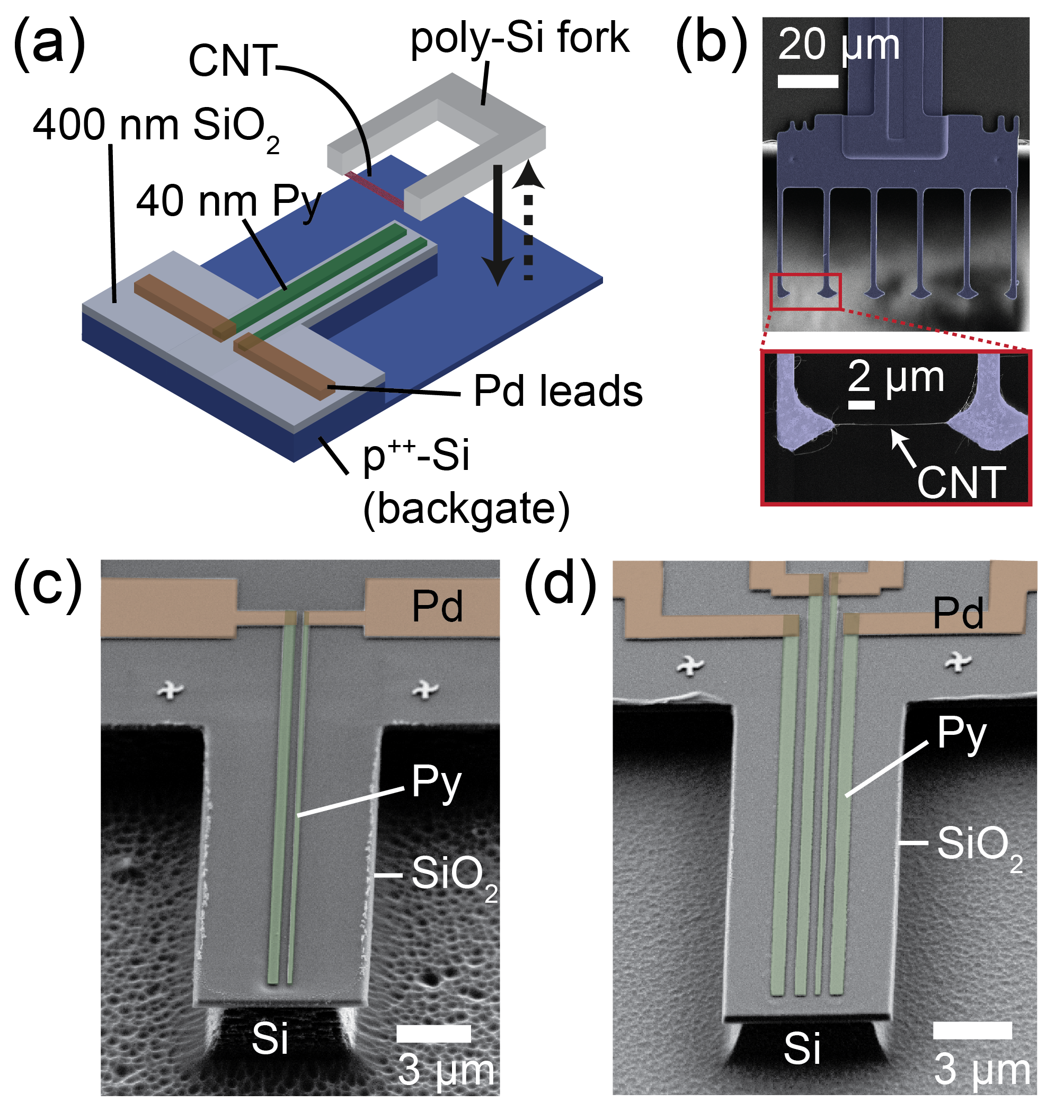
Figure 1 (a) summarizes the dry transfer of pristine CNTs onto prefabricated ‘electrical circuit chips’. Following Refs. 4; 5; 6; 7, the electrical circuit preparation is detached from the growth of the CNTs, done separately on a ‘transfer chip’. We transfer the CNTs only in the last fabrication step under a light microscope and ambient conditions in a process called fork stamping, which allows the precise placement of a single CNT onto a suited, predefined electrical circuit Muoth and Hierold (2012); Ranjan et al. (2015). Figure 1 (c) shows our electrical circuit chip consisting of a mesa structure with two ferromagnetic Py source-drain (SD) electrodes, a heavily p-doped Silicon (Si) wafer acting as backgate and Palladium (Pd) leads. As schematically depicted in Fig. 1 (a), a moveable Si fork structure, with ideally a single CNT grown across it, is pushed down on the predefined mesa structure (black arrow) while at the same time monitoring the current through the ferromagnetic SD contacts. Once contact has been detected and established, the fork is retracted (dashed arrow), ideally leaving an individual pristine CNT suspended over the ferromagnetic contacts. To immediately characterize the CNT device, we measure the differential conductance as a function of the backgate voltage. Undesired CNTs can then be removed by applying large SD bias voltages and the stamping procedure is repeated until an optimal CNT is found.
CNT growth on optimized transfer chip with retractable poly-Si forks
CNTs are grown separately from the electrical circuit on a transfer chip with polycrystalline silicon fork structures, following previously reported protocols Muoth and Hierold (2012); Muoth et al. (2010). Figure 1 (b) shows a scanning electron microscopy (SEM) image of such a fork structure protruding beyond the edge of the transfer chip. Each fork consists of multiple, wide, thick poly-Si arms and can be retracted beyond the wafer edge, allowing to use different forks on the same transfer chip in one transfer session. CNTs are grown via chemical vapor deposition across the wide gaps between the fork arms by using iron-loaded ferritin proteins as catalyst precursors Muoth et al. (2010); Durrer et al. (2009). At best, one obtains maximally one individual CNT spanning each gap between the fork arms as visible in the zoom-in SEM image of Fig. 1 (b), for which the catalyst concentration has to be optimized on reference forks Muoth and Hierold (2012). Electron microscopy is omitted on the actual transfer chips to avoid carbon deposition, and to maintain the pristine, as-grown character of the transferred CNTs.
Fabrication of mesa structure and electrodes on electrical circuit chip
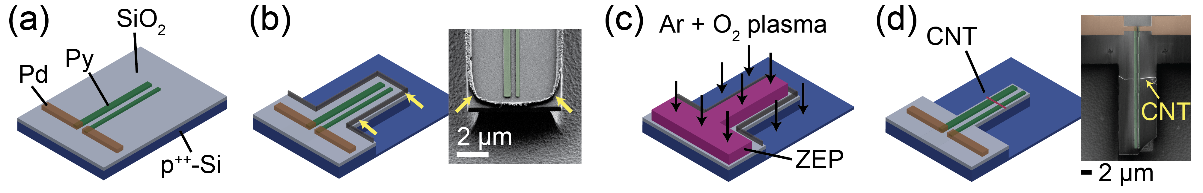
The electrical circuit chip with the mesa structure and the ferromagnetic contacts is fabricated independently of the transfer chip in a five-step electron-beam lithography (EBL) process (Fig. 2). We use a heavily p-doped Si wafer with a nm thick thermal oxide top layer as substrate. After the deposition of Au markers, two long, nm thin ferromagnetic Py electrodes of variable width are patterned with a pitch of nm by a previously optimized EBL step with ZEP520A resist, thermal electron gun evaporation and lift-off process Samm et al. (2014). The use of thin, high aspect ratio Py contacts allows us to obtain single-domain contacts with the magnetic easy axis along the strip direction and accurately control the coercive or switching fields by the width of the contacts Aurich et al. (2010). Here, we choose nm and nm wide Py strips to obtain well separated switching fields of the electrodes Samm et al. (2014). The Py strips are contacted by nm thick Pd leads in another EBL step (see Fig. 2 (a)). This results in a geometry suited for spin-valve experiments in the quantum dot (QD) regime at low temperatures Sahoo et al. (2005); Aurich et al. (2010); Samm et al. (2014), where the heavily p-doped Si wafer can be used as a backgate to tune the chemical potential of the QD. For creating the mesa structure in the SiO2/Si, we first spin-coat a m thick PMMA 950k resist layer as etching mask. This resist is exposed and developed by EBL, leaving the mesa structure and Py electrodes protected. For etching into the SiO2/Si around the mesa structure, we use an optimized, anisotropic and selective reactive ion etching (RIE) process Legtenberg et al. (1995) in an Oxford Plasmalab 80 Plus system, resulting in a T-shaped etch profile (compare Fig. 1 (c)). First, a min. long CHF3 RIE etching is used for the removal of the nm thick SiO2 layer with a flow of sccm CHF3, pressure mTorr and power W, leading to an etching selectivity of compared to the resist mask. A subsequent min. anisotropic and selective SF6/O2 RIE with a flow of sccm SF6 and sccm O2, mTorr, power W and an etching selectivity of compared to the resist creates a m deep trench in the p-doped Si. The anisotropic profile stems from a Si sidewall passivation by oxygen species during the etching process Legtenberg et al. (1995), which also leads to the observed porous structure in the Si. Before lift-off, the resist mask is typically etched down to a thickness of nm in an Ar/O2 RIE step to minimize residues from the etch process. After the lift-off procedure in warm N-Methyl-2-pyrrolidone (NMP) or acetone, we typically encounter large carbon-fluor polymer residues close to the edge of the mesa structure (arrows in Fig. 2 (b)) which severely hinder a successful CNT transfer. These residues originate from polymerization and passivation layers formed in the CHF3/SF6 RIE etching on the side of the resist mask Kim and Jeon (2006) and are not removable by the solvents in the lift-off process. We found that the selectivity of the etch process is optimal only in a narrow parameter range and cannot be optimized simultaneously to protect the mesa without residues. Sonication to remove the residues mechanically, as used in Ref. 10, typically leads to a partial collapse of the mesa structure and affects the sensitive Py strips. We remove these polymer residues using a 5th EBL process: Spincoating another nm thick ZEP520A resist layer on the wafer covers the entire mesa structure with the Py strips and the residues. We only expose and develop areas close to the edge of the mesa structure in another EBL step, resulting in a mask open only in the area of the residues, as sketched in Fig. 2 (c). The residues can thus be reproducibly removed in a standard Ar/O2 plasma without exposing the Py strips to O2 plasma. After another lift-off procedure this results in clean, m wide and m high mesa structures etched into the SiO2/Si substrate, which allow access for the CNT fork stamping. Figure 1 (c) and (d) show two different realized geometries, one with two ferromagnetic contact electrodes, the other with four. While in the first geometry only a mechanical transfer of the CNTs can be implemented, the 4-terminal geometry can also be used for an electrical cutting of the CNT described in detail later, or, alternatively, for non-local spin experiments similar to graphene Tombros et al. (2007). The comparatively wide mesa relative to the fork gap improves the CNT transfer, while the T-shaped underetched mesa profile is beneficial for avoiding CNT-induced electrical shorts from the contacts to the p-doped backgate. To monitor the current through the SD contacts during CNT transfer, all electrical circuit chips are glued into chip carriers and wire-bonded prior to the transfer of CNTs. Figure 2 (d) shows a schematic and SEM image of a device after successful CNT transfer, demonstrating that single CNTs (yellow arrow) can be transferred onto ferromagnetic contacts.
CNT transfer
In the final fabrication step, the CNTs are transferred from the fork structures onto the electrical circuit chip Muoth and Hierold (2012). Immediately prior to the CNT transfer, the electrical circuit chips with the ferromagnetic Py electrodes have to be cleaned from surface oxides in a s long Argon plasma etch. This step is crucial, since without it no electrical contact is formed due to contamination and oxidation of the electrodes. The transfer is done using a micro-manipulator setup under ambient conditions. To reduce further oxidation, a nitrogen flow is applied around the electrical circuit chip. The transfer chip - with the CNT forks protruding beyond the edge of the wafer - is carefully mounted on a three axis piezo controlled transfer arm. Next, the forks with CNTs are carefully aligned with the mesa structure using an optical microscope. Finally, the fork is pressed down over the mesa structure and the contacts (black arrow in Fig. 1 (a)). Simultaneously, we monitor the current through two SD terminals in a voltage-biased setup. In contrast to previous experiments with normal Pd or Au electrodes Muoth and Hierold (2012); Waissman et al. (2013); Ranjan et al. (2015), we have to apply relatively large SD voltages of V to electrically register every CNT ‘touch-down’ event when a CNT bridges the SD contacts, carefully studied by SEM on reference samples following the transfer. When a successful contact is detected, there are two ways to deposit the CNT. First, it can be mechanically torn off by keeping the fork pushed down and retracting it parallel to the chip surface using the built-in mechanism, leaving the CNT in place and suspended over the SD contacts due to van-der-Waals forces. Second, in a 4-terminal device (Fig. 1 (d)), the CNT can be selectively cut between the outer pair of contacts using large electrical currents, following the approach of Ref. 7. In the pushed-down state of the transfer fork, the application of a large voltage between the two outer pairs of contacts (while maintaining the inner ones on the same potential) breaks the CNT at a single point between each of the two outer contact pairs due to Joule heating Waissman et al. (2013). The transfer fork can then be lifted, leaving only a part of the CNT suspended over the inner contacts. Typical cutting currents for single wall CNTs are on the order of , consistent with Ref. 7. Usually, we obtain room temperature device resistances of for a single CNT. The contacts can already be annealed during stamping by driving the SD voltage up and down, a process which will be described in detail in the next section. In case that the resistance is too low () - meaning that bundles or several CNTs were transferred, as inferred from SEM images of reference samples - the CNTs can be removed by applying a large SD bias voltage. In the cutting procedure for the 4-terminal geometry discussed above, this is immediately evident when one observes several steps in the monitored IV-curves or much higher currents than are required to cut the CNT. After the removal of undesired CNTs, the electrical circuit chip can be used again for further transfers until an optimal CNT is found. Already during transfer, we observe that stamped CNT devices on ferromagnetic Py contacts degrade to a much higher device resistance on the timescale of a few minutes, often reaching values as high as when the device had an original resistance of . This suggests that the surfaces of the Py contacts oxidize fast. The exposure of samples to air between the CNT transfer under nitrogen flow and the mounting of samples in our cryogenic measurement setup is thus reduced to a minimum.
III Electrical characterization
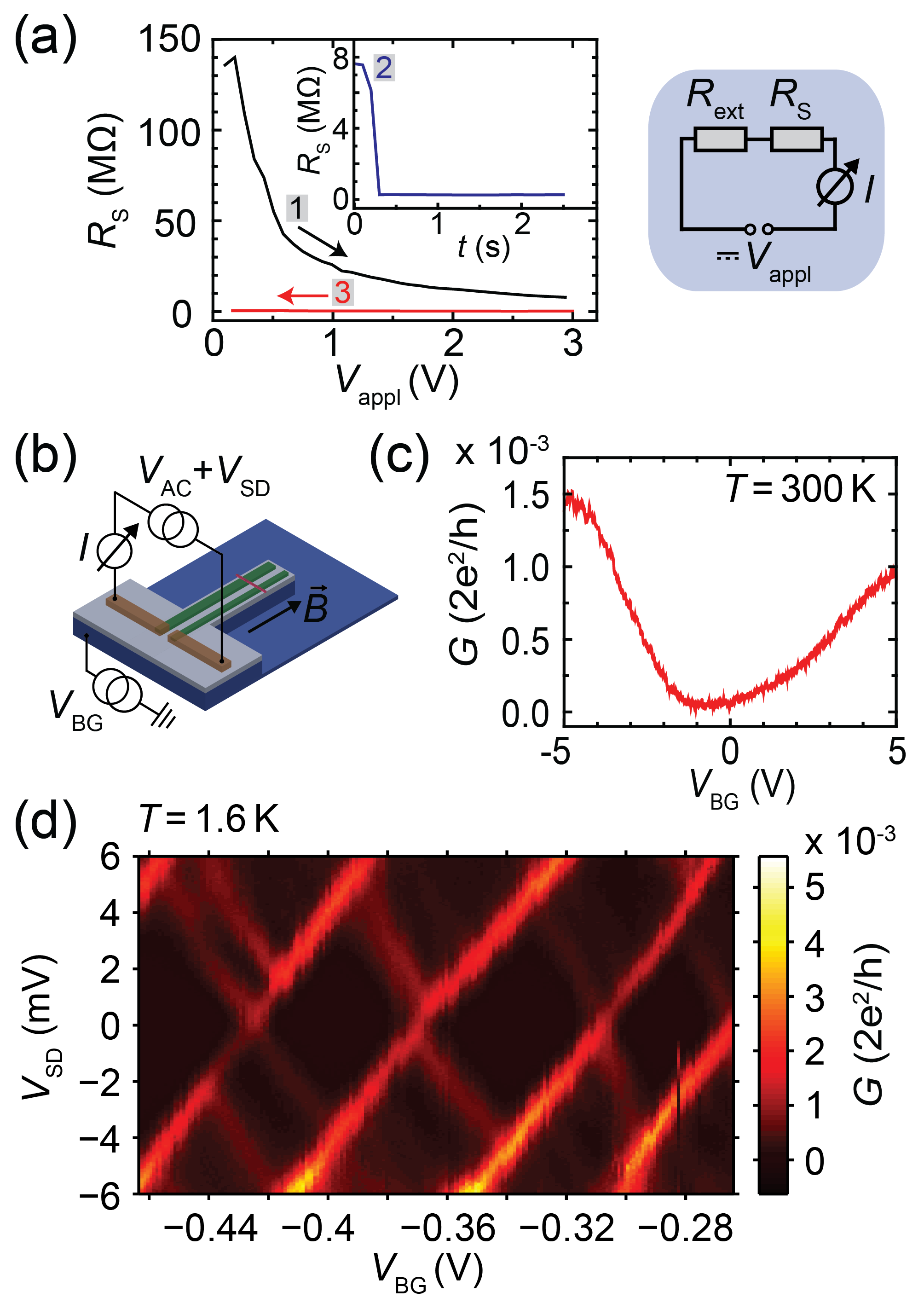
The already wire-bonded CNT devices are built into a cryogenic variable temperature insert allowing measurements in the range of K. Samples usually degrade and have a relatively high resistance compared to the values directly after CNT transfer. To measure a signal at low temperatures, the devices have first to be annealed in the cryostat at room temperature and in low-pressure He atmosphere. Fig. 3 (a) shows the electrical circuit for annealing and a typical ‘annealing trace’. A DC voltage is applied over an external resistor in series with the sample , measuring the current, from which can be calculated. A typical annealing cycle consists of ramping the voltage up to some predefined value (black trace 1), a waiting trace at for a given time (blue trace 2) and the backtrace (red curve 3). This is repeated several times with increasing until a device resistance change to reasonable values in the range is observed. Figure 3 (a) shows the traces of a successful annealing, with a large device resistance at the start and a final device resistance of originating from the abrupt change in the waiting trace (2) at V (inset). In contrast to the current annealing usually applied for suspended graphene devices where the cleaning and device changes are ascribed to Joule heating Moser et al. (2007), it is evident that such large resistance changes can only be caused by the contact resistance, showing that the annealing is actually not only cleaning the CNT, but mainly a contact resistance change. We note that the currents through the device prior to the resistance change are in the sub-A regime. These characteristics are similar for most samples with device resistance changes often occurring after a certain waiting time at and agree very well with previous findings on surface-oxidized Pd/PdO contacts to CNTs Jones et al. (2006). We speculate that a large voltage portion drops across the contact interfaces, leading to an irreversible dielectric breakdown in the oxide barrier on the Py surface, possibly creating permanent percolation paths to the CNT Jones et al. (2006); Lombardo et al. (2005). This results in a low impedance CNT device with relatively transparent contacts. For further electrical characterization, we use the measurement setup depicted in Fig. 3 (b). We measure the differential conductance using standard lock-in amplifiers as a function of the backgate voltage or source drain bias in a spin-valve geometry. To characterize the metallic or semiconducting nature of the stamped CNT, we measure at room temperature as function of , seen in Fig. 3 (c) for a semiconducting CNT. Figure 3 (d) shows the charge stability diagram of such a device at K, where we measure as a function of backgate voltage and the bias. Clear Coulomb Blockade (CB) diamonds are visible, indicating that a single QD forms in the CNT suspended over the two SD contacts. From the measurements, we can extract a backgate leverarm of eV/V only slightly smaller than for CNTs on substrate, a charging energy meV and from the excited states a level spacing of meV. From the extracted level spacing, we can roughly estimate an effective QD size of Nygård et al. (1999), in reasonable agreement with the designed contact pitch and center-to-center separation of nm, respectively nm.
IV Magnetoresistance
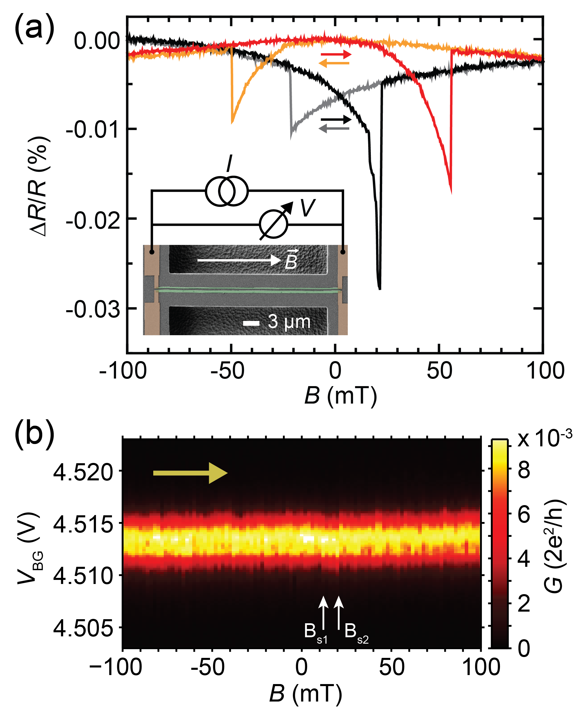
We perform local magnetoresistance measurements at K in a standard QD spin-valve geometry. First, to characterize the quality of the ferromagnetic Py strips after processing, we perform anisotropic magnetoresistance (AMR) measurements following Refs. 24; 27. For this, we use the sample geometry and measurement setup depicted in the inset of Fig. 4 (a). Here, the m long Py strips reside on a mesa bridge structure surrounded by trenches in the SiO2/Si on two sides only, enabling transport measurements through each strip separately. It is possible to transfer CNTs also on this structure by tilting the transfer forks. We measure the resistance through individual Py strips while ramping the external magnetic field applied parallel to the strip axis. Figure 4 (a) shows the respective up- and downsweep (arrows) for a (red/orange) and nm (black/grey) wide Py strip. Sharp resistance changes at mT for the wide and mT for the narrow Py strip indicate a sign reversal of the magnetization. These values agree very well with our previous strip characterization on flat substrates Aurich et al. (2010); Samm et al. (2014). The sharp switching indicates that the bulk behavior of the magnetization remains intact after processing. To assess the magnetoresistance (MR) through the CNT, we measure MR maps over a single CB conductance maximum Samm et al. (2014), see Fig. 4 (b). Here, the conductance through the CNT is plotted as a function of the backgate voltage for the up-sweep of (large arrow). For this peculiar device with and nm wide Py strips, we expect switching fields of mT Samm et al. (2014) and mT, indicated by vertical arrows in Fig. 4 (b). A small change in amplitude and position of the CB conductance maximum might be visible at these positions, but the data remain inclusive for a reliable interpretation. The MR signal of a spin-valve device is proportional to the conductance change between the parallel and antiparallel magnetization configuration of the two contacts. We would expect a MR signal of for Py Samm et al. (2014), but the conductance noise of the device coming from both amplitude and position fluctuations of the CB resonances is on the same order of magnitude or larger. Further repetitions of up- and downsweeps on the same and other devices show similar features also with different switching fields. The conductance noise and instability of the devices, also apparent in the charge stability diagram of Fig. 3 (d), are still too large to detect reliably any spin signals in the CNT spin-valves. We speculate that these fluctuations of the CB resonances are caused by instabilities in the contact interfaces. The annealing curves clearly show that the ferromagnetic contact interfaces are not completely stable due to oxidation and might have inherent charge traps in the oxide, possibly close to the contact area. The current difficulties in magnetoresistance experiments can be overcome by using an in-situ setup similar to the one used in Ref. 7, using less oxidizing ferromagnetic materials as e.g. PdNi alloys or implementing oxygen tight tunnel barriers on top of the ferromagnetic contacts prior to a CNT transfer. Hexagonal boron nitride (hBN), for example, holds great promise for longer spin-life times in bottom-up fabricated CNT spin-valve devices, an approach currently followed intensively for graphene spin-valves Fu et al. (2014); Drögeler et al. (2014).
V Conclusions
We report a fabrication scheme suited for the mechanical transfer of individual CNTs onto ferromagnetic contacts, leading to pristine, as-grown CNTs suspended over ferromagnetic electrodes in a spin-valve geometry. This fabrication scheme can be readily extended to other contact materials, including complicated device layouts with several gates and superconducting as well as ferromagnetic electrodes, enabling the combination of ultra-clean QD systems with hybrid-CNT devices. Using these recipes, we demonstrate that single CNTs can be contacted on top of ferromagnetic contacts with reasonable device resistances achieved by an electrical contact annealing, and that we are able to form single QDs suited for transport studies at low temperatures. No clear spin-valve signal could be found yet in magnetoresistance experiments at low temperatures, which we tentatively ascribe to interface properties resulting in an increased conductance noise.
Acknowledgements.
We thank S. Ilani, A. Bachtold, V. Ranjan, G. Puebla-Hellmann and J. Samm for fruitful discussions. The CNT stamping was done in the FIRST lab of ETHZ. We acknowledge generous access to that facility. This work was financially supported by the Swiss National Science Foundation (SNF), the Swiss Nanoscience Institute (SNI), the Swiss NCCR QSIT, the ERC project QUEST and the EU FP7 project SE2ND.References
- Cao et al. (2005) J. Cao, Q. Wang, and H. Dai, Nat. Mater. 4, 745 (2005).
- Kuemmeth et al. (2008) F. Kuemmeth, S. Ilani, D. C. Ralph, and P. L. McEuen, Nature 452, 448 (2008).
- Steele et al. (2009a) G. A. Steele, G. Gotz, and L. P. Kouwenhoven, Nat. Nanotechnol. 4, 363 (2009a).
- Wu et al. (2010) C. C. Wu, C. H. Liu, and Z. Zhong, Nano Lett. 10, 1032 (2010).
- Muoth and Hierold (2012) M. Muoth and C. Hierold, in IEEE 25th International Conference on Micro Electro Mechanical Systems (MEMS), Paris (IEEE, 2012) pp. 1352–1355.
- Pei et al. (2012) F. Pei, E. A. Laird, G. A. Steele, and L. P. Kouwenhoven, Nat. Nanotechnol. 7, 630 (2012).
- Waissman et al. (2013) J. Waissman, M. Honig, S. Pecker, A. Benyamini, A. Hamo, and S. Ilani, Nat. Nanotechnol. 8, 569 (2013).
- Jung et al. (2013) M. Jung, J. Schindele, S. Nau, M. Weiss, A. Baumgartner, and C. Schönenberger, Nano Lett. 13, 4522 (2013).
- Viennot et al. (2014) J. J. Viennot, J. Palomo, and T. Kontos, Appl. Phys. Lett. 104, 113108 (2014).
- Ranjan et al. (2015) V. Ranjan, G. Puebla-Hellmann, M. Jung, T. Hasler, A. Nunnenkamp, M. Muoth, C. Hierold, A. Wallraff, and C. Schönenberger, Nat. Commun. , accepted (2015).
- Cao et al. (2004) J. Cao, Q. Wang, M. Rolandi, and H. Dai, Phys. Rev. Lett. 93, 216803 (2004).
- Steele et al. (2013) G. A. Steele, F. Pei, E. A. Laird, J. M. Jol, H. B. Meerwaldt, and L. P. Kouwenhoven, Nat. Commun. 4, 1573 (2013).
- Laird et al. (2013) E. A. Laird, F. Pei, and L. P. Kouwenhoven, Nat. Nanotechnol. 8, 565 (2013).
- Steele et al. (2009b) G. A. Steele, A. K. Hüttel, B. Witkamp, M. Poot, H. B. Meerwaldt, L. P. Kouwenhoven, and H. S. J. van der Zant, Science 325, 1103 (2009b).
- Benyamini et al. (2014) A. Benyamini, A. Hamo, S. V. Kusminskiy, F. von Oppen, and S. Ilani, Nat. Phys. 10, 151 (2014).
- Herrmann et al. (2010) L. G. Herrmann, F. Portier, P. Roche, A. Levy Yeyati, T. Kontos, and C. Strunk, Phys. Rev. Lett. 104, 026801 (2010).
- Schindele et al. (2012) J. Schindele, A. Baumgartner, and C. Schönenberger, Phys. Rev. Lett. 109, 157002 (2012).
- J-D. Pillet et al. (2010) J-D. Pillet, C. H. L. Quay, P. Morfin, C. Bena, A. Levy Yeyati, and P. Joyez, Nat. Phys. 6, 965 (2010).
- Sahoo et al. (2005) S. Sahoo, T. Kontos, J. Furer, C. Hoffmann, M. Gräber, A. Cottet, and C. Schönenberger, Nat. Phys. 1, 99 (2005).
- Braun et al. (2005) M. Braun, J. König, and J. Martinek, Europhys. Lett. 72, 294 (2005).
- S.-N. Zhang et al. (2012) S.-N. Zhang, W. Pei, T.-F. Fang, and Q.-f. Sun, Phys. Rev. B 86, 104513 (2012).
- Stadler et al. (2014) P. Stadler, W. Belzig, and G. Rastelli, Phys. Rev. Lett. 113, 047201 (2014).
- Braunecker et al. (2013) B. Braunecker, P. Burset, and A. Levy Yeyati, Phys. Rev. Lett. 111, 136806 (2013).
- Aurich et al. (2010) H. Aurich, A. Baumgartner, F. Freitag, A. Eichler, J. Trbovic, and C. Schönenberger, Appl. Phys. Lett. 97, 153116 (2010).
- Muoth et al. (2010) M. Muoth, T. Helbling, L. Durrer, S.-W. Lee, C. Roman, and C. Hierold, Nat. Nanotechnol. 5, 589 (2010).
- Durrer et al. (2009) L. Durrer, J. Greenwald, T. Helbling, M. Muoth, R. Riek, and C. Hierold, Nanotechnology 20, 355601 (2009).
- Samm et al. (2014) J. Samm, J. Gramich, A. Baumgartner, M. Weiss, and C. Schönenberger, J. Appl. Phys. 115, 174309 (2014).
- Legtenberg et al. (1995) R. Legtenberg, H. Jansen, M. de Boer, and M. Elwenspoek, J. Electrochem. Soc. 142, 2020 (1995).
- Kim and Jeon (2006) S. B. Kim and H. Jeon, J. Korean Phys. Soc. 49, 1991 (2006).
- Tombros et al. (2007) N. Tombros, C. Jozsa, M. Popinciuc, H. T. Jonkman, and B. J. van Wees, Nature 448, 571 (2007).
- Moser et al. (2007) J. Moser, A. Barreiro, and A. Bachtold, Appl. Phys. Lett. 91, 163513 (2007).
- Jones et al. (2006) F. E. Jones, A. A. Talin, F. Léonard, P. M. Dentinger, and W. M. Clift, J. Electron. Mater. 35, 1641 (2006).
- Lombardo et al. (2005) S. Lombardo, J. H. Stathis, B. P. Linder, K. L. Pey, F. Palumbo, and C. H. Tung, J. Appl. Phys. 98, 121301 (2005).
- Nygård et al. (1999) J. Nygård, D. H. Cobden, M. Bockrath, P. L. McEuen, and P. E. Lindelof, Appl. Phys. A 69, 297 (1999).
- Fu et al. (2014) W. Fu, P. Makk, R. Maurand, M. Bräuninger, and C. Schönenberger, J. Appl. Phys. 116, 074306 (2014).
- Drögeler et al. (2014) M. Drögeler, F. Volmer, M. Wolter, B. Terrés, K. Watanabe, T. Taniguchi, G. Güntherodt, C. Stampfer, and B. Beschoten, Nano Lett. 14, 6050 (2014).