Electronic response of graphene to linelike charge perturbations
Abstract
The problem of electrostatic screening of a charged line by undoped or weakly doped graphene is treated beyond the linear-response theory. The induced electron density is found to be approximately doping independent, , at intermediate distances from the charged line. At larger , twin - junctions may form if the external perturbation is repulsive for graphene charge carriers. The effect of such inhomogeneities on conductance and quantum capacitance of graphene is calculated. The results are relevant for transport properties of graphene grain boundaries and for local electrostatic control of graphene with ultrathin gates.
I Introduction
One of the properties that make graphene an attractive platform for electronic devices is tunability of its charge carrier density through electrostatic gating. The gates can be brought into immediate proximity of graphene, which enables one to control doping of this material very efficiently. Local gating on ultrasmall lengthscales is attainable by utilizing nanowire Young and Kim (2009) or nanotube Ni et al. (2015) gates [Fig. 1(a)]. Physical insight into fundamental characteristics of such devices can be gained from a simplified problem of how graphene responds to a linelike external charge [Fig. 1(c)]. This problem is also relevant for understanding properties of grain-boundary defects [Fig. 1(b)] in graphene grown by chemical-vapor deposition. Biró and Lambin (2013); Cummings et al. (2014); Yazyev and Chen (2014)
The problem of screening of a linelike charge by electrons in graphene is an interesting challenge because the usual linear-response theory Radchenko et al. (2013) fails when the line is highly charged and/or when graphene is lightly doped. Previous studies of one-dimensional charge perturbations in graphene eschewed solving this difficult problem resorting instead to ad hoc approximations for the induced carrier density profile. Young and Kim (2009); Fei et al. (2013) Accurate determination of this profile requires numerical calculations, e.g., finding the self-consistent solution of the Dirac equation for electron wavefunctions and the Poisson equation for the electrostatic potential as a function of the in-plane coordinate transverse to the charged line. However, if varies smoothly on the scale of the local Fermi length , a simpler approach based on the Thomas-Fermi approximation (TFA) can be applied. Landau and Lifshitz (1991) We show that approximate solutions of the TFA equations for the electron density can be derived in certain limits. Using these analytical solutions and numerical simulations, we compute two other important observables amenable to experimental probes: the conductance and the gate capacitance.
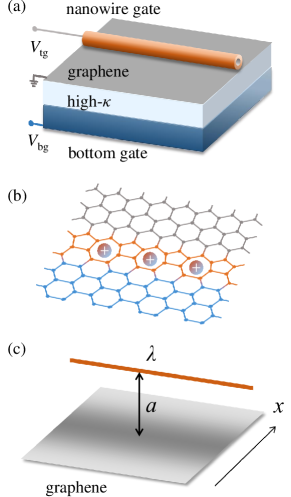
Let us introduce our key notations and assumptions. We denote the linear charge density of the external perturbation by . Without loss of generality, we take to be positive (unless specified otherwise). We assume that the unperturbed electron density of graphene is uniform. To distinguish between -type and -type doping, we define the Fermi momentum corresponding to as a signed quantity,
| (1) |
We assume that the external charge has a Lorentzian density distribution,
| (2) |
The actual profile of the external charge may of course be somewhat different. For example, the charge distribution of a grain boundary probably does not have power-law tails. However, the role of parameter in Eq. (2) is mainly to regularize the response of graphene at very short distances, Fogler et al. (2007) i.e., it serves as a short-distance cutoff. As long as we are not interested in microscopic physics at , Eq. (2) can be adopted as a convenient model. In all examples mentioned above (nanowire and nanotube gates and also grain boundaries in graphene) realistically achievable can be as small as a few nanometers. The particular functional form of Eq. (2) corresponds to the idealized model shown in Fig. 1(c) where the external charge is located off the graphene plane and is truly one-dimensional. This can be seen from the fact that the electrostatic potential created in the graphene plane by the out-of-plane charged line is equal to that created by the in-plane Lorentzian charge distribution (2):
| (3) | ||||
| (4) |
In general, the effective width parameter should be taken as the larger of the actual physical width of the charge distribution and its distance to the graphene plane. In this article we assume that electron-electron interaction in graphene is weak, i.e., we consider the dimensionless coupling constant a small parameter in the problem. Kotov et al. (2012) Here is the graphene Fermi velocity. By choosing a substrate with a large dielectric constant [Fig. 1(a)], it is possible to make significantly smaller than unity. However, it is difficult to make truly small, so as a rule we do not treat as a small parameter. Finally, we assume that the graphene is not too highly doped,
| (5) |

Depending on the relation between , , and , the response of graphene can be either weak or strong and either linear or nonlinear (Fig. 2). The degree of nonlinearity is controlled by the dimensionless parameter
| (6) |
Linear screening is realized if (the bottom part of the ‘weak’ region in Fig. 2) where the induced electron density
| (7) |
scales linearly with . On the other hand, if , the response is nonlinear. A conspicuous manifestation of the nonlinearity is found in the region labeled ‘strong’ in Fig. 2, where the induced density can be approximated by a ‘universal’ (doping-independent) form . In the large- ‘asymptotic’ regime of Fig. 2, the induced density exhibit a power-law decay
| (8) |
where the dependence of on is linear [Eq. (11) of Sec. II] if is small and logarithmic if is large [Eq. (27)]. The ‘perfect’ screening region is included in Fig. 2 for completeness. Here graphene maintains charge neutrality locally, i.e., the induced density is close to the external one, , so that the model assumption (2) must be critically revisited.
The crossovers among the predicted screening regimes can be systematically studied in experiments using devices that have both top and bottom gates, Fig. 1(a). High linear charge densities with are quite feasible to achieve with top gate voltages . For lightly doped graphene, , the corresponding is deep in the nonlinear regime.
In the remainder of this article we derive detailed formulas for the carrier density profiles, verify them by numerical simulations, then make predictions for capacitance and transport measurements.
II Linear response
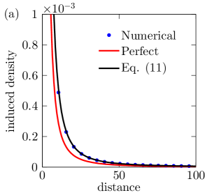
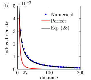
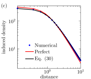
Linear screening of linelike charges by doped graphene has been studied in previous literature. Radchenko et al. (2013) We include a brief summary of the relevant results for later comparison with our nonlinear response theory. Linear screening is realized when the external charge is not too high or when graphene doping level is not too low. The quantitative criterion is derived below. Within the linear-response theory, the induced electron density is given by
| (9) |
where the term is the Fourier transform of the effective external charge [Eq. (2)] at momentum . As we are primarily concerned with distances where the TFA is valid, the dielectric function of graphene can be approximated by Kotov et al. (2012); Ando et al. (2002); Wunsch et al. (2006)
| (10) |
A particularly simple analytical expression for can be derived in the ‘asymptotic’ regime, cf. Fig. 2. Carrying out the integration in Eq. (9) by the steepest-descent method, one finds the leading-order approximation for the induced density to be Radchenko et al. (2013)
| (11) |
(In contrast, for a pointlike charge perturbation. Wunsch et al. (2006)) Note that the coefficient in Eq. (11) is much larger than under the assumed condition (5), so that . Such an ‘overshoot’ is typical for screening of localized perturbations in metals. Metallic systems possess the overall charge neutrality. However, at distances shorter than the local screening length from the perturbation screening is necessarily weak. Therefore, there is a missing charge at short distances, which has to be compensated at large . However, the electric field is not overscreened: it is of the same sign as the external one but reduced in magnitude.
The analytical Eq. (11) agrees well with our numerical simulations shown in Fig. 3(a). For these simulations we used previously developed codes Zhang and Fogler (2008) with suitable modifications. In brief, the electron density to be found was defined on a grid of with periodic boundary conditions. The solution was obtained by minimizing the total energy of the system (kinetic plus electrostatic) within the TFA using standard technical computing software. MAT
Refinement of Eq. (10) can be obtained through the random-phase approximation (RPA). Within the RPA, the dielectric function of graphene coincides with Eq. (10) at but at it is given by a different formula Ando et al. (2002); Wunsch et al. (2006)
| (12) |
Notably, becomes doping independent at where the response is dominated by virtual interband transitions. (For corrections to the last result beyond RPA, see Refs. Kotov et al., 2012; Sodemann and Fogler, 2012.)
Substituting Eq. (12) in Eq. (9) and using contour integration techniques to evaluate the integral, we find the RPA correction to :
| (13) | ||||
| (14) |
which is a particular case of the Friedel oscillations. Ashcroft and Mermin (1976) At intermediate distances, Eq. (9) yields Radchenko et al. (2013)
| (15) |
Finally, let us estimate the region of validity of the linear-response theory. This theory applies if the induced carrier density is smaller than the original one, or, equivalently, if the local Fermi momentum,
| (16) |
is perturbed slightly compared to [Eq. (1)]. Naively, one may require the condition to hold at all distances of interest, . In fact, the validity region is wider because the nonlinearity affects only the response at momenta . (As mentioned above, the response at is essentially doping-independent.) Therefore, the smallest number we should use in the argument of for our estimate is . From Eqs. (7), (15), and (16) we get
| (17) |
Neglecting the logarithmic factor, which is never large in practice, we arrive at as the criterion of linear screening.
III Nonlinear response
In this Section we treat a more difficult case where screening is nonlinear. Our approach to this problem is to solve the TFA equations analytically and numerically. The first of these equations is
| (18) |
where
| (19) |
is the local chemical potential of graphene (assuming the linear Dirac dispersion of quasiparticles). The second equation links the total charge density and the electrostatic potential,
| (20) |
This relation can be inverted by exploiting techniques from the theory of analytic functions:
| (21) |
where stands for the Cauchy principal value. If desired, Eqs. (18)–(21) can be combined into a single nonlinear integral equation for . The TFA is valid if Landau and Lifshitz (1991)
| (22) |
The problem we want to solve can be separated into two parts, depending on whether is greater or smaller than . The latter situation occurs at large , where we expect screening behavior akin to linear response. Indeed, it is easily seen that follows Eq. (8) provided the integral in Eq. (21) is dominated by . Invoking Eq. (18), we then obtain the asymptotic behavior for , where
| (23) |
and is to be determined below.
The analytical form of at is not immediately obvious. Fortunately, were are able to find (by trial and error) the following approximate solution:
| (24) |
which is characterized by a nonlinear screening length . This length is found from the argument that at small the external field is nearly unscreened, so that the total and the external potentials differ only by some constant: [Eq. (4)]. Comparing with Eq. (24) at , we get
| (25) |
From Eqs. (22) and (25) we see that Eq. (24) is valid at . At smaller the density and the Fermi momentum presumably tend to a finite maximum, i.e,
| (26) |
The last logarithmic factor is valid if ; otherwise, it should be replaced by a number of the order of unity. Equation (26) is consistent with Eq. (17) for the linear regime. Hence, in both regimes the nonlinearity parameter [Eq. (6)] has the physical meaning of the maximum relative change in the Fermi momentum caused by the perturbation.
To fix the so far undetermined coefficient , we require a smooth matching of Eq. (8) and Eq. (24), which yields
| (27) |
More accurate expression for can be obtained by iterations using Eq. (24) as the input to the TFA equations. Namely, substituting it into Eq. (18), we can get , which we can then insert into Eq. (21) to obtain an improved approximation for . The first iteration yields
| (28) |
which demonstrates a good agreement with our numerical simulations, see Fig. 3(b).
For completeness, we consider the case of
| (29) |
where nonlinear screening affects distances shorter than our cutoff length . At such large , a highly doped region appears at , where screening is nearly perfect, i.e., where the difference between and is relatively small and the system is able to maintain the local charge neutrality. The solution for can again be obtained by iterations. The input to Eq. (21) is now . The first correction is
| (30) |
Its range of validity can be estimated from the requirement that at this correction is no longer small, which implies
| (31) |
Furthermore, one can check that at Eq. (30) matches by the order of magnitude with given by Eq. (24) with set to . This leads to us conclude that at Eq. (24) and then at Eq. (8) must still hold with . Because of the exponentially large magnitude of , we could verify numerically only the case. Comparison of simulations with Eq. (30) in Fig. 3(c) indeed shows a good agreement.
When and have opposite signs, twin - junctions appear at . The density profile near a graphene - junction has been studied in Ref. Zhang and Fogler, 2008. These results should more or less carry over to the present problem, so they will not be repeated. In the following Sections we focus on computing the effect of nonlinear screening on transport and capacitance characteristics of the system.
IV Quantum Capacitance
The charge density is a natural parameter for graphene grain boundaries [Fig. 1(b)]. In contrast, linelike perturbation created by means of narrow gates [Fig. 1(a)] are controlled by the voltage with respect to graphene while has to be found by integrating the differential gate capacitance
| (33) |
It is important that is not simply equal to the electrostatic potential difference between the gate and the graphene sample. It has another contribution from the graphene chemical potential:
| (34) |
As a result, the differential gate capacitance has two components, the classical (or geometrical) one and the so-called quantum one , which add in series:
| (35) |
Our goal in this Section is to derive the quantum capacitance of a device with an ultranarrow top gate, Fig. 1(a). However, it is useful to review the conventional planar-gate geometry first. Here the classical capacitance per unit area is inversely proportional to the separation between graphene and the planar gate. In turn, the quantum capacitance is proportional to the thermodynamical density of states, . This quantity can also be written in terms of the inverse Thomas-Fermi screening length :
| (36) |
The net result of having a finite screening length is equivalent to replacing the physical gate-graphene separation by an effective one:
| (37) |
Although in this article we use the free-fermion approximation [Eq. (10)] for the linear-response screening length , in reality it is modified by many-body interactions and disorder (see, e.g., Refs. Fogler, 2004; Allison et al., 2006). Recently quantum capacitance measurements have been used to probe such effects of graphene. Yu et al. (2013); Basov et al. (2014)
If the gate is now a long metallic string or radius , the capacitances per unit length are relevant. In order to derive we start with a general expression for the electrostatic potential difference between the string and the graphene sample,
| (38) |
which follows from Eqs. (3) and (20). If we set , we obtain . Hence, the geometric capacitance of the system is
| (39) |
which can be alternatively derived by the method of images. Next, combining Eqs. (18), (20), (33), (34), (38), and subtracting , we find
| (40) |
We can now use this expression for analytical and numerical calculations. Our analytical formulas for positive are as follows:
| , | (41a) | ||||
| , | (41b) |
where is the exponential integral. These equations describe, respectively, the linear and the ‘strong’ regimes of Fig. 2. They can be commonly written as
| (42) |
where is equal to (in the same order) and . We conclude that the total capacitance can be modeled after the geometric one,
| (43) |
with the effective gate-graphene separation
| (44) |
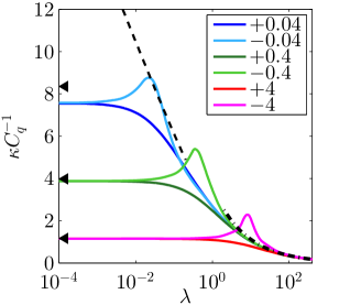
where on the right-hand side was added by hand to recover the result expected for a perfect metal, . The similarity of Eqs. (37) and (44) illustrates once again that quantum capacitance is a measure of the screening length of a system. Whereas in the planar-gate geometry this length is formally divergent for undoped graphene, for the linelike gate the divergence is regularized by nonlinearity. Numerically, we find that as a function of approaches a universal envelope curve (41b) shown by the dashed line in Fig. 4.
For completeness, we consider the ‘perfect’ screening regime where
| (45) |
for all relevant , so that Eq. (40) becomes
| (46) |
The inverse thermodynamic density of states in Eqs. (45) and (46) is to be evaluated at . For where the integrand scales as , we find the analytical result
| (47) |
which agrees with our numerical simulations (the dashed-dotted curve in Fig. 4).
If is negative, i.e., if and have opposite signs, the twin - junctions form at some which can be estimated from Eq. (17) setting to zero. This event — the onset of the ambipolar regime — is marked by a maximum in , which is absent in the unipolar trace for the same , see Fig 4. From dimensional arguments, as approaches zero, the height of the maximum in measured with respect to its plateau at should approach a universal number. Figure 4 suggests that number is about . However, such dimensional arguments assume the TFA is valid, which, similar to the case of a single - junction, Zhang and Fogler (2008) is the case at small . To treat a more typical case one needs to go beyond the TFA, which may be a problem for future research.
V Conductance
Charged linelike defects are known to significantly influence electron transport in graphene. Grain boundaries strongly reduce the sheet conductivity of large-area graphene, Tsen et al. (2012) while bipolar junctions created by nanowire gates cause conductance oscillations. Young and Kim (2009) In this section we find expressions for the graphene conductance relevant for both situations.
We consider a scattering problem for a massless Dirac particle with initial momentum subject to the potential perturbation
| (48) |
The intermediate equation follows from the TFA, Eq. (18). For a weak potential, we can apply the standard perturbation theory to the massless Dirac equation to obtain the reflection coefficient
| (49) |
which is similar to the first Born approximation formula for the Schrödinger equation. Landau and Lifshitz (1991) The region of validity of this formula can be extended beyond the perturbative regime if in the argument of the exponential we replace by , the local momentum at the point where the scattering potential is the ‘most’ nonanalytic. Landau and Lifshitz (1991) However, this is permissible only if is real at all , i.e., if all points on the quasiparticle path are classically allowed (no quantum tunneling occurs).
The conductance is found by summing the transmittances of all the channels:
| (50) |
In the absence of scattering, , the conductance is
| (51) |
where is the width of the graphene sheet. Assuming , we can compute at by replacing the summation with the integration over . However, diverges as tends to , so that the first Born approximation cannot be used. In fact, the absolute value of the exact reflection coefficient must be approaching unity instead of diverging. We account for this by cutting off the integration limits at where :
| (52) |
For the linear screening regime, [Eq. (6)], we obtain
| (53) |
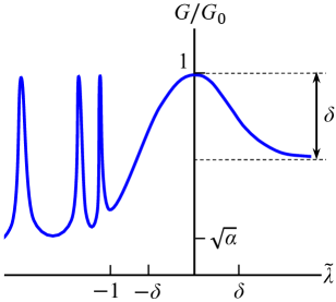
Accordingly, the conductance as a function of exhibits an asymmetric maximum at drawn schematically in Fig. 5. The asymmetry becomes pronounced when approaches , where the screening begins to cross over into the nonlinear regime. If is positive, becomes essentially independent of . Using Eqs. (24) and (26) and changing the integration variable in Eq. (49) one can show that does not depend on any more in this regime. Actually, this is clear from dimensional argument: since is dimensionless, it may not depend on , which has the units of inverse length. This implies that ceases to decrease with , leveling at a plateau, . If is negative, the situation is quite different. The scattering potential is repulsive. At large it causes the twin - junctions to appear at [Eq. (27)], which act as tunneling barriers. Here even the modified Born approximation fails completely. The transmittance of each - junction is given instead by Cheianov and Fal’ko (2006)
| (54) |
where
| (55) |
is the electric field at the junction, Zhang and Fogler (2008) with being the density gradient. Combining these equation, we obtain
| (56) |
Multiple reflections of the quasiparticles in the region between the - junctions lead to the conductance oscillations and resonances. The net transmittance is given approximately by the Fabry-Pérot-like formula Young and Kim (2009)
| (57) |
where is the phase acquired by a quasiparticle after one roundtrip between the junctions:
| (58) |
The last estimate is obtained using Eqs. (24) and (27). Conductance minima arise at , where is an integer. They have the magnitude because the transmittance of each junction is appreciable only at small angles Cheianov and Fal’ko (2006) , cf. Eq. (56). Conductance maxima are found at , which correspond to . The widths of these maxima and the distance from one to the next increase exponentially as a function of . The heights of these maxima approach , which is a manifestation of the resonant tunneling phenomenon. In practice, observation of the resonant tunneling requires samples with the mean free path longer than the roundtrip distance ; otherwise, the conductance is influenced by diffusive transport between and across the - junctions. Fogler et al. (2008) In previous experiments with nanowire-gated graphene devices, Young and Kim (2009) the conductance maxima were found to be significantly lower than and decreasing with the top gate voltage, i.e., , presumably due to disorder scattering.
If the conductance can also be measured in the direction parallel to the gate, we expect it to show a dependence consisting of a smooth increase with with superimposed small oscillations due to quantization of the quasi-bound resonant modes. This oscillating part would have the same period as the Fabry-Pérot oscillations in the transverse conductance discussed above. At small gate voltages, both longitudinal and transverse conductances are expected to show additional fine features related to the analog of the Goos-Hänchen effect in graphene, Beenakker et al. (2009) which is a lateral displacement of a quasiparticle trajectory along the - interface during reflection. This effect can be included using a more accurate equation for that incorporates both the path length contribution expressed by Eq. (58) and the phase shift of the reflections at the - interfaces.
VI Discussion
In this work we considered linelike charged perturbations on graphene and derived analytical expressions for the induced density profiles in both linear and nonlinear screening regimes. These results were applied to the analysis of two types of electronic properties. The first one is the quantum correction to the classical capacitance between the narrow gate and graphene as a function of the top gate voltage. Measuring this quantity will be a direct way for observing the crossovers among different screening regimes and testing our predictions. For example, we showed that the divergence of the inverse quantum capacitance of undoped graphene predicted from the naive linear-response theory will be curbed by nonlinear screening effects. If the gate creates a strong repulsive potential for charge carriers in graphene, it can induce twin - junctions. Our calculations indicate that the onset of this ambipolar regime is signaled by a peak in the inverse quantum capacitance.
The second quantity we studied is the transverse electrical conductance of the system. Our predictions for the ambipolar regime, where the conductance oscillates as a function of gate voltage, include formulas for the maxima, minima, and the oscillation period. Our theory holds in the ballistic transport regime, which was difficult to probe in earlier experiments on such systems. Young and Kim (2009) We hope that modern higher-quality devices that utilize graphene encapsulated in boron nitride Dean et al. (2010) and single-wall nanotube gates of smallest possible diameter, would enable a systematic investigation of nonlinear screening and resonant tunneling phenomena we discussed.
Conductance of graphene with charged grain boundaries was previously studied analytically and numerically in Refs. Ferreira et al., 2011; Radchenko et al., 2013; Ihnatsenka and Zozoulenko, 2013. In Ref. Radchenko et al., 2013 transport properties were computed modeling charged grain boundaries as short line segments of length . However, the screening was treated assuming that the boundaries are infinitely long, which seems to require the opposite inequality. These incompatible assumptions make a direct comparison between our analytical results for the conductance difficult. As for screening, only the linear regime was considered in Ref. Radchenko et al., 2013, and for this our results agree.
Our findings have further implication for experiments using novel scanned-probe techniques. Linear charged defects in the form of grain boundaries have been shown to reflect surface plasmon polaritons Fei et al. (2013); Schnell et al. (2014); Gerber et al. (2014) and induce photocurrent, Woessner et al. (2015) both of which can be imaged with nanoscale resolution using scanning near-field optical microscopy. Scanning tunneling microscopy is another avenue of approach to measure local density of states. Koepke et al. (2013); Nemes-Incze et al. (2013) We will apply our theory to interpretation of such measurements in a future work. Ni et al. (2015)
Finally, let us comment on the proposals Katsnelson and Novoselov (2007) that graphene is a condensed-matter laboratory for exotic effects predicted in other fields of physics. For example, electronic response of graphene to a pointlike charge has an interesting analogy to the atomic collapse of superheavy elements. Pomeranchuk and Smorodinsky (1945); Zeldovich and Popov (1972) It has been shown Katsnelson (2006); Novikov (2007); Shytov et al. (2007a, b); Fogler et al. (2007); Pereira et al. (2007); Kotov et al. (2012) that in graphene subcritical and supercritical charges produce qualitatively different behavior of the screened electrostatic potential at large distances from the perturbation, the critical charge being of the order of . Characteristic oscillations of the local density of states that appear in the supercritical case have been recently detected experimentally. Wang et al. (2013) Phenomena similar to atomic collapse have been also studied theoretically in the context of narrow-band gap semiconductors and Weyl semimetals. Kolomeisky et al. (2013) In turn, our problem of screening of a linelike charge perturbation in graphene have interesting analogies in cosmology (screening of a hypothetical cosmic string by vacuum polarization Nascimento et al. (1999)) and polyelectrolyte physics (Onsager-Manning condensation of counterions Manning (1969); Oosawa (1968)). Our results imply that in graphene nonlinear screening plays a greater role for linelike charges compared to the pointlike ones: the former are always supercritical, e.g., there is no threshold for the appearance of Friedel oscillations. Finally, our analytical formulas assume , which can be realized using a high- dielectric substrate [Fig. 1(a)], such as SrTiO3 [Refs. Couto et al., 2011; Das Sarma and Li, 2012; Sachs et al., 2014; Saha et al., 2014]. For such gate dielectrics it may be important to consider electric-field dependence of in nonlinear screening regimes. Fu et al.
Acknowledgements.
The work has been supported by the Office of the Naval Research and by the University of California Office of the President. We thank D. N. Basov, Z. Fei, and G. Ni for prior and ongoing collaborations that motivated this study and also A. Ferreira and B. I. Shklovskii for useful discussions and comments on the manuscript.References
- Young and Kim (2009) A. F. Young and P. Kim, Nature Phys. 5, 222 (2009).
- Ni et al. (2015) G. Ni, B.-Y. Jiang, M. Bockrath, C.-N. Lau, M. M. Fogler, and D. N. Basov, “Tunable plasmonic reflectors in graphene nanostructures with carbon nanotube gates,” (2015), unpublished.
- Biró and Lambin (2013) L. P. Biró and P. Lambin, New J. Phys. 15, 035024 (2013).
- Cummings et al. (2014) A. W. Cummings, D. L. Duong, V. L. Nguyen, D. Van Tuan, J. Kotakoski, J. E. Barrios Vargas, Y. H. Lee, and S. Roche, Adv. Mat. 26, 5079 (2014).
- Yazyev and Chen (2014) O. V. Yazyev and Y. P. Chen, Nature Nano. 9, 755 (2014).
- Radchenko et al. (2013) T. M. Radchenko, A. A. Shylau, I. V. Zozoulenko, and A. Ferreira, Phys. Rev. B 87, 195448 (2013).
- Fei et al. (2013) Z. Fei, A. S. Rodin, W. Gannett, S. Dai, W. Regan, M. Wagner, M. K. Liu, A. S. McLeod, G. Dominguez, M. Thiemens, A. H. Castro Neto, F. Keilmann, A. Zettl, R. Hillenbrand, M. M. Fogler, and D. N. Basov, Nature Nano. 8, 821 (2013).
- Landau and Lifshitz (1991) L. D. Landau and E. M. Lifshitz, Quantum Mechanics: Non-Relativistic Theory, 3rd ed., edited by E. M. Lifshitz and L. P. Pitaevskii (Butterworth-Heinemann, Amsterdam, 1991).
- Fogler et al. (2007) M. M. Fogler, D. S. Novikov, and B. I. Shklovskii, Phys. Rev. B 76, 233402 (2007).
- Kotov et al. (2012) V. N. Kotov, B. Uchoa, V. M. Pereira, F. Guinea, and A. H. Castro Neto, Rev. Mod. Phys. 84, 1067 (2012).
- Ando et al. (2002) T. Ando, Y. Zheng, and H. Suzuura, J. Phys. Soc. Jpn. 71, 1318 (2002).
- Wunsch et al. (2006) B. Wunsch, T. Stauber, F. Sols, and F. Guinea, New J. Phys. 8, 318 (2006).
- Zhang and Fogler (2008) L. M. Zhang and M. M. Fogler, Phys. Rev. Lett. 100, 116804 (2008).
- (14) MATLAB Release 2012b, The MathWorks, Inc., Natick, Massachusetts.
- Sodemann and Fogler (2012) I. Sodemann and M. M. Fogler, Phys. Rev. B 86, 115408 (2012).
- Ashcroft and Mermin (1976) N. Ashcroft and N. Mermin, Solid State Physics (Saunders College, Philadelphia, 1976).
- Fogler (2004) M. M. Fogler, Phys. Rev. B 69, 121409(R) (2004).
- Allison et al. (2006) G. Allison, E. A. Galaktionov, A. K. Savchenko, S. S. Safonov, M. M. Fogler, M. Y. Simmons, and D. A. Ritchie, Phys. Rev. Lett. 96, 216407 (2006).
- Yu et al. (2013) G. L. Yu, R. Jalil, B. Belle, A. S. Mayorov, P. Blake, F. Schedin, S. V. Morozov, L. A. Ponomarenko, F. Chiappini, S. Wiedmann, U. Zeitler, M. I. Katsnelson, A. K. Geim, K. S. Novoselov, and D. C. Elias, Proc. Natl. Acad. Sci. USA 110, 3282 (2013).
- Basov et al. (2014) D. N. Basov, M. M. Fogler, A. Lanzara, F. Wang, and Y. Zhang, Rev. Mod. Phys. 86, 959 (2014).
- Tsen et al. (2012) A. W. Tsen, L. Brown, M. P. Levendorf, F. Ghahari, P. Y. Huang, R. W. Havener, C. S. Ruiz-Vargas, D. A. Muller, P. Kim, and J. Park, Science 336, 1143 (2012).
- Cheianov and Fal’ko (2006) V. V. Cheianov and V. I. Fal’ko, Phys. Rev. B 74, 041403(R) (2006).
- Fogler et al. (2008) M. M. Fogler, D. S. Novikov, L. I. Glazman, and B. I. Shklovskii, Phys. Rev. B 77, 075420 (2008).
- Beenakker et al. (2009) C. W. J. Beenakker, R. A. Sepkhanov, A. R. Akhmerov, and J. Tworzydło, Phys. Rev. Lett. 102, 146804 (2009).
- Dean et al. (2010) C. R. Dean, A. F. Young, I. Meric, C. Lee, L. Wang, S. Sorgenfrei, K. Watanabe, T. Taniguchi, P. Kim, K. L. Shepard, and J. Hone, Nature Nano. 5, 722 (2010).
- Ferreira et al. (2011) A. Ferreira, X. Xu, C.-L. Tan, S.-K. Bae, N. M. R. Peres, B.-H. Hong, B. Özyilmaz, and A. H. Castro Neto, Europhys. Lett. (EPL) 94, 28003 (2011).
- Ihnatsenka and Zozoulenko (2013) S. Ihnatsenka and I. V. Zozoulenko, Phys. Rev. B 88, 085436 (2013).
- Schnell et al. (2014) M. Schnell, P. S. Carney, and R. Hillenbrand, Nature Commun. 5, 3499 (2014).
- Gerber et al. (2014) J. A. Gerber, S. Berweger, B. T. O’Callahan, and M. B. Raschke, Phys. Rev, Lett. 113, 055502 (2014).
- Woessner et al. (2015) A. Woessner, P. Alonso-Gonzalez, M. B. Lundeberg, G. Navickaite, Y. Gao, Q. Ma, D. Janner, K. Watanabe, T. Taniguchi, V. Pruneri, P. Jarillo-Herrero, J. Hone, R. Hillenbrand, and F. H. Koppens, “Non-invasive photocurrent nanoscopy on bare and hexagonal boron nitride encapsulated graphene,” (2015), unpublished.
- Koepke et al. (2013) J. C. Koepke, J. D. Wood, D. Estrada, Z.-Y. Ong, K. T. He, E. Pop, and J. W. Lyding, ACS Nano 7, 75 (2013).
- Nemes-Incze et al. (2013) P. Nemes-Incze, P. Vancsó, Z. Osváth, G. I. Márk, X. Jin, Y.-S. Kim, C. Hwang, P. Lambin, C. Chapelier, and L. P. Biró, Carbon 64, 178 (2013).
- Katsnelson and Novoselov (2007) M. Katsnelson and K. Novoselov, Solid State Commun. 143, 3 (2007).
- Pomeranchuk and Smorodinsky (1945) I. Y. Pomeranchuk and Y. A. Smorodinsky, J. Phys. USSR 9, 97 (1945).
- Zeldovich and Popov (1972) Y. B. Zeldovich and V. S. Popov, Sov. Phys. Uspekhi 14, 673 (1972).
- Katsnelson (2006) M. I. Katsnelson, Phys. Rev. B 74, 201401 (2006).
- Novikov (2007) D. S. Novikov, Phys. Rev. B 76, 245435 (2007).
- Shytov et al. (2007a) A. V. Shytov, M. I. Katsnelson, and L. S. Levitov, Phys. Rev. Lett. 99, 236801 (2007a).
- Shytov et al. (2007b) A. V. Shytov, M. I. Katsnelson, and L. S. Levitov, Phys. Rev. Lett. 99, 246802 (2007b).
- Pereira et al. (2007) V. M. Pereira, J. Nilsson, and A. H. Castro Neto, Phys. Rev. Lett. 99, 166802 (2007).
- Wang et al. (2013) Y. Wang, D. Wong, A. V. Shytov, V. W. Brar, S. Choi, Q. Wu, H.-Z. Tsai, W. Regan, A. Zettl, R. K. Kawakami, S. G. Louie, L. S. Levitov, and M. F. Crommie, Science 340, 734 (2013).
- Kolomeisky et al. (2013) E. B. Kolomeisky, J. P. Straley, and H. Zaidi, Phys. Rev. B 88, 165428 (2013).
- Nascimento et al. (1999) J. R. S. Nascimento, I. Cho, and A. Vilenkin, Phys. Rev. D 60, 083505 (1999).
- Manning (1969) G. S. Manning, J. Chem. Phys. 51, 924 (1969).
- Oosawa (1968) F. Oosawa, Biopolymers 6, 135 (1968).
- Couto et al. (2011) N. J. G. Couto, B. Sacépé, and A. F. Morpurgo, Phys. Rev. Lett. 107, 225501 (2011).
- Das Sarma and Li (2012) S. Das Sarma and Q. Li, Solid State Commun. 152, 1795 (2012).
- Sachs et al. (2014) R. Sachs, Z. Lin, and J. Shi, Sci. Rep. 4, 3657 (2014).
- Saha et al. (2014) S. Saha, O. Kahya, M. Jaiswal, A. Srivastava, A. Annadi, J. Balakrishnan, A. Pachoud, C.-T. Toh, B.-H. Hong, J.-H. Ahn, T. Venkatesan, and B. Özyilmaz, Sci. Rep. 4, 6173 (2014).
- (50) H. Fu, K. V. Reich, and B. I. Shklovskii, “Collapse of electrons to a donor cluster in SrTiO3,” arXiv:1504.03675 (unpublished).