Phonon-limited carrier mobility and resistivity from carbon nanotubes to graphene
Abstract
Under which conditions do the electrical transport properties of one-dimensional (1D) carbon nanotubes (CNTs) and 2D graphene become equivalent? We have performed atomistic calculations of the phonon-limited electrical mobility in graphene and in a wide range of CNTs of different types to address this issue. The theoretical study is based on a tight-binding method and a force-constant model from which all possible electron-phonon couplings are computed. The electrical resistivity of graphene is found in very good agreement with experiments performed at high carrier density. A common methodology is applied to study the transition from 1D to 2D by considering CNTs with diameter up to 16 nm. It is found that the mobility in CNTs of increasing diameter converges to the same value, the mobility in graphene. This convergence is much faster at high temperature and high carrier density. For small-diameter CNTs, the mobility strongly depends on chirality, diameter, and existence of a bandgap.
I Introduction
Graphene and carbon nanotubes (CNTs) are respectively two-dimensional (2D) and one-dimensional (1D) allotropes of pure carbon. Their remarkable physical and chemical properties have been studied extensivelySaito98 ; Charlier07 ; Jorio07 ; Castro09 but investigations of the electrical transport in graphene and CNTs are usually done separately. Of course, it is known that graphene is a semi-metal characterized by Dirac cones at the charge neutrality point while CNTs can either be metallic or semiconducting depending on their chirality. Carrier mobilities in graphene and CNTs may reach very high values, which make them promising for high-frequency applications. However, record values differ considerably between graphene ( cm2/V/s)Morozov08 ; Bolotin08 ; Castro09 and semiconducting CNTs ( cm2/V/s).Zhou05 ; Ho10 ; Biswas11 Furthermore, one should in principle recover the transport properties of graphene by increasing the diameter of metallic or semiconducting CNTs, at least in situations where this transport is only limited by intrinsic processes like phonon scattering. Quite suprisingly, this transition of the transport properties from 1D to 2D has never been carefully investigated even if there are numerous studies on the electron-phonon coupling in the two materials.Saito98 ; Charlier07 ; Castro09 ; Woods00 ; Suzuura02 ; Jiang05 ; Jorio07 ; Machon06 ; Ferrari07 ; Stauber07 ; Suzuura08 ; Hwang08 ; Castro10 ; Perebeinos10 ; Borysenko10 ; Attaccalite10 ; Kaasbjerg12 ; Park14
In this work, we study the evolution of the phonon-limited mobility of carriers from CNTs to graphene, i.e., from 1D to 2D. We calculate the electrical mobility (or resistivity) using a common methodology, enabling a direct comparison between graphene and semiconducting/metallic CNTs of varying diameters. We focus on phonon scattering not only because it is a limiting mechanism at high carrier density and high temperature Efetov10 but also because it is intrinsic to the materials, at variance with scattering by impurities or by surface optical phonons of nearby oxides, which are dependent on the geometry, on the quality of the materials and on the nature of the environment. We also leave aside carbon nanoribbons in this study, since the possible existence of edge states does not allow for a straightforward analysis of the 1D to 2D transistion.
In the following, we present fully atomistic calculations of the phonon-limited mobility in graphene and CNTs with diameter up to 16 nm. We show that the mobility in CNTs tends to the limit in graphene at large diameter (sometimes above 10 nm), but that the route to it strongly depends on size, chirality, and temperature. These behaviors are explained by specific features of the band structure and of the electron-phonon coupling.
II Methodology
II.1 Justification of the methodology
A strong motivation for this study is that it sheds light on the effects of confinement and dimensionality upon the electron/phonon band structures, the electron-phonon coupling and the transport. For example, the scattering of carriers in 1D semiconductor nanostructures such as nanowires is merely limited to back-scattering when only one electronic band is populated. This tends to reduce the scattering probability. At the same time, confinement leads to an enhancement of the electron-phonon coupling, which is stronger in 1D than in 2D (and 3D).Luisier09 ; Zhang10 ; Neophytou11 In this context, it is particularly interesting to investigate these effects in 1D and 2D carbon allotropes since their band structures considerably differ from those of usual semiconductor nanostructures. In addition, it is important to understand how (and when) the phonon-limited carrier mobility in CNTs of increasing diameter approaches the limit in graphene as a function of temperature, carrier density, chirality, and metallic or semiconducting character.
There are already numerous theoretical studies on the phonon-limited transport in graphene Stauber07 ; Hwang08 ; Castro10 ; Mariani10 ; Perebeinos10 ; Kaasbjerg12 ; Park14 and CNTs Suzuura02 ; Perebeinos05 ; Torres06 ; Popov06 ; Kauser07 ; Pennington07 ; Charlier07 ; Koswatta07 ; Zhao09 but it is only in recent works on graphene that the couplings to all phonons have been calculated from first-principles without extracting parameters from experiments.Borysenko10 ; Kaasbjerg12 ; Park14 From these works, we learn that it is essential to consider many different phonon modes like longitudinal acoustic (LA), transverse acoustic (TA) and optical phonons to predict the temperature- and density-dependent resistivity of graphene. We deduce that it is likely the case for CNTs, especially because the selection rule is broken in the direction perpendicular to the CNT axis, in particular in small-diameter CNTs.
Therefore it is essential to consider all possible electron-phonon scattering processes to predict the phonon-limited mobility in CNTs. In order to catch the 1D-2D transition, it is also necessary to go well beyond previous calculations that were limited to small-diameter tubes. However, first-principles calculations cannot be performed on large-diameter CNTs because the computational cost increases dramatically with the number of atoms per unit cell. In this work, we present calculations combining tight-binding (TB) and force-constant models for electrons and phonons, respectively. The parameters of these models were refined on the latest first-principles calculations.Park14 ; Mauri14 The low-field mobility is computed taking all electron and phonon bands into account, the carriers being coupled to all possible phonons, including intra- and inter-subband scattering. We show that this approach gives results for graphene in excellent agreement with first-principles calculationsPark14 ; Mauri14 and with experiments.Efetov10 ; Zou10 The same methodology is then applied to CNTs. In the following, we present results for -type graphene and CNTs, i.e., for the transport of holes. Very similar results are found for electrons. For the sake of comparison, carrier densities are given as equivalent surface densities (in cm-2). For a CNT of diameter , the 1D and 2D carrier densities are related by .
II.2 Tight-binding Hamiltonian
The electronic states of graphene and CNTs are written in the basis of the orbitals where is the axis perpendicular to the lattice. Interactions are restricted to first-nearest-neighbors (1NNs). The Hamiltonian matrix is therefore defined by two quantities, the onsite energy and the 1NN hopping term that both depend on the atomic displacements induced by the phonons. The variations of are governed by a power law Harrison89
| (1) |
in which and are the actual and equilibrium bond lengths between 1NN atoms, respectively. The parameters in Eq. (1) were set based on the GW calculation data in Ref. Mauri14, , i.e. Å, eV, (which gives m/s for the Fermi velocity,) and , (which fits the canonical acoustic gauge field, eV).
The variations of the onsite term with atomic displacements were ignored in most previous TB studies Perebeinos05 ; Stauber07 ; Mariani10 ; Perebeinos10 arguing that they give little contribution to the deformation potentials. In our case, we follow the arguments of Ref. Niquet09, and introduce in a term proportional to the average of the relative bond length variation
| (2) |
where the sum is over the three 1NN atoms. The Dirac point at is taken as the origin of the electronic energies. The parameter in Eq. 2 is set to eV, and has been extracted from Density Functional Theory (DFT) calculations of the band structure of graphene for different cell sizes. These DFT calculations were performed with the BigDFTBigDFT code, using Norm-Conserving PseudopotentialsHGH-K and the Generalized Gradient ApproximationPBE for the exchange and correlation potential. BigDFT makes use of a systematic real-space wavelet basis, and can handle surface-like boundary conditions,PSolver which allows to define a common energy reference for all cell sizes and enables a direct comparison of energy levels.Note
The changes in due to bond length variations (Eq. 1) contribute to the coupling of electrons to both LA and TA phonons, whereas those in (Eq. 2) are only relevant for LA phonons. Their respective influence on the mobility was heavily debatedWoods00 ; Perebeinos05 ; Stauber07 ; Mariani10 ; Perebeinos10 ; Suzuura02 but it is now clear that both of them must be taken into account.Park14
In the case of CNTs, the hopping terms between 1NN orbitals slightly vary from one bond to another due to the curvature.Dresselhaus05 ; Kane97b ; Charlier07 As a consequence, there is a small curvature-induced gap in ”metallic” zigzag CNTs scaling as . For example, we obtain gaps of 80, 45, and 29 meV in (9,0), (12,0), and (15,0) CNTs, respectively, in excellent agreement with experiments.Ouyang01 For symmetry reasons, armchair CNTs always preserve their metallic character.Dresselhaus05 ; Kane97b ; Charlier07 The hybridization induced by the curvature Blase94 is neglected in the present calculations.
II.3 Phonons
For the calculation of the phonons, the dynamical matrix is built by a fourth-nearest-neighbour (4NN) force-constant model as originally fitted to experimental data by Jishi et al.Jishi93 and later fitted to ab-initio calculations and enhanced by off-diagonal force-constants for the 2NN.Wirtz04 For the current calculations, we refitted the model, taking also the off-diagonal elements of the 4NN into account. The importance of the 4NN off-diagonal elements had already been noted before in ab-initio phonon calculations.Dubay While the phonon-dispersion itself can be fitted very well without the off-diagonal terms, they have an important impact on the phonon modes: they are necessary to obtain the correct amplitude for the admixture of optical components to the acoustic phonon modes at non-vanishing wave-vector. This admixture considerably influences the contribution of the acoustic modes to the mobility.Mauri14 For example, the ratio of the acoustic phonon deformation potential with and without optical phonon mixing is about % in our model, which is comparable to the one in Ref. Mauri14, . The parameters of our force-constant model and the dispersion obtained from it are given in Appendix A.
II.4 Electron-phonon coupling
The same parameters are used for the calculations of the electron and phonon band structures of CNTs and graphene – there is no additional parameter.
Following Ref. Zhang10, , the matrix element for the transition of an electron from an initial state to a final state after emission of a phonon (same formula for absorption) is given by
| (3) |
where and are the wave vectors of the electron and phonon, respectively, while and are the indexes of the electron band and phonon mode. is an eigenvector element of the electronic Hamiltonian at equilibrium, where (or ) is the atom index in the unit cell. is the atomic orbital centered on atom in the unit cell . is an eigenvector element of phonon state and is the corresponding eigenfrequency. is the component (,,) of vector , is the number of Wigner-Seitz unit cells, and is the mass of a carbon atom. The transition rate is given by Fermi’s golden rule,
| (4) |
where is the energy of and is the equilibrium phonon occupation number (Bose-Einstein distribution).
The electron-phonon scattering rates are calculated for all electronic bands within at least +200 meV of the Fermi level, and for all phonon modes.
II.5 Mobility
The low field mobility is obtained by the resolution of the Boltzmann transport equation in the stationary regime. Under the application of a constant electric field , the distribution function in the state is given to the first-order in by where is the Fermi-Dirac distribution function. In CNTs, is solution of the following equations:
| (5) |
where is the group velocity along the electric field and is the length of the CNT. The mobility is then given by
| (6) |
The linearized Boltzmann transport equation is solved exactly. Brillouin zone integrations are performed on a non-homogeneous 1D grid for CNTs and on an triangular mesh for graphene (e.g., 8600 -points in 1D and 17124 triangles in 2D for a surface carrier density of cm-2 and K).
III Results and discussion
III.1 Application to graphene
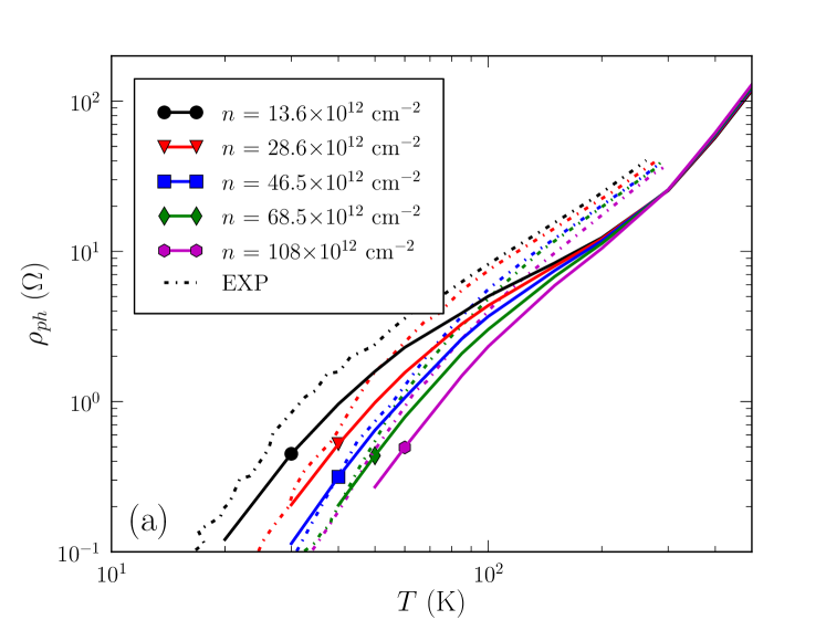
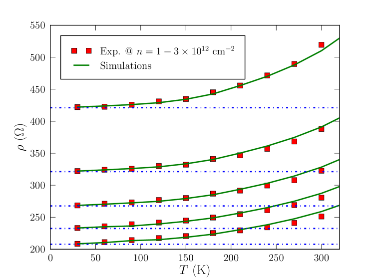
Figure 1 presents the electrical resistivity of graphene calculated versus temperature , for several carrier densities . In accordance with early theoretical predictionsHwang08 and experiments, Efetov10 the resistivity is proportional to at low temperature, while at higher temperature it varies linearly with (the threshold strongly depends on ). In the regime, short wavelength acoustic phonons are frozen out, restricting scattering processes to small scattering angles.Hwang08 ; Efetov10 In agreement with DFT calculations,Park14 both LA and TA phonons contribute to the scattering in the and regimes. We also confirm that: i) in the regime and above, the resistivity does not depend on ;Hwang08 ; Efetov10 ii) at room temperature and above, the resistivity is enhanced by optical phonon scattering Borysenko10 ; Park14 so that it deviates from the trend.
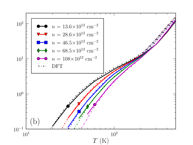
In Ref. Efetov10, , the resistivity of graphene was measured at high carrier density ( cm-3). Its temperature dependent component is displayed in Fig. 1 and is compared to our predictions. The agreement between theory and experiments is fairly good. As shown in Appendix B, in this range of carrier density, the resistivity is mainly limited by (intrinsic) phonon scattering, justifying the comparison. Also, the agreement is excellent with the DFT calculations of Ref. Park14, (Fig. 1b).
In Appendix B, we show that our predicted resistivities also agree with the experimental data of Ref. Zou10, measured at lower carrier density. In that case, we have to include scattering by the surface optical (SO) phonons of the substrate. We also demonstrate in Appendix B that scattering by intrinsic phonons becomes more efficient than scattering by SO phonons not only at low temperature because it involves lower energy phonons, but also at high temperature and high carrier density where SO phonon potentials are efficiently screened.
III.2 Carrier mobility in CNTs
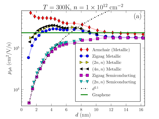
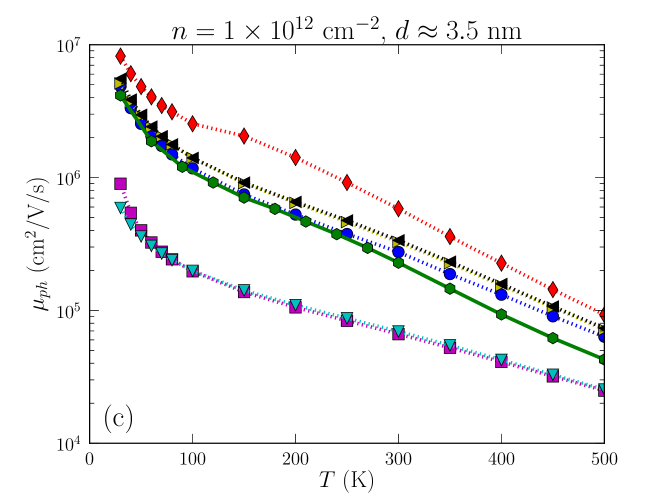
We consider now zigzag , armchair , chiral and chiral CNTs. and CNTs are always metallic. Zigzag and chiral CNTs are metallic when is a multiple of 3, semiconducting otherwise. As discussed above, a gap is induced by the curvature in small-diameter metallic CNTs. The electronic band structures of CNTs (Appendix C) are intimately related to that of graphene.Saito98 ; Charlier07 In the 2D space of graphene, the 1D vectors allowed for CNTs form a bundle of parallel lines along the tube direction, the separation between the lines being inversely proportional to the CNT diameter. This results in CNT band structures composed of successive subbands, one for each line. In these conditions, since carrier transport takes place within an energy window of a few around the Fermi surface, we anticipate that the transport properties of CNTs can reach those of graphene in three ways, namely by increasing 1) the tube diameter, 2) the carrier density, or 3) the temperature. In the three cases, the number of subbands in the transport energy window will increase in such a way that the 1D transport will progressively turn into 2D transport – the quantification of perpendicular to the tube axis becoming irrelevant. Figure 2 illustrates the evolution of the mobility along the three ways. It shows that the mobility in CNTs actually tends to its limit in graphene but with very different behaviors depending on the nature of the CNTs. The reasons why are discussed below.
III.2.1 Mobility versus diameter
The carrier mobility in CNTs calculated for cm-2 and K is plotted as a function of the diameter in Fig. 2a. The mobility is considerably smaller in semiconducting CNTs with nm than in metallic ones, and is also much smaller than in graphene for the same carrier density. This is mainly due to the non-zero mass of the carriers since the bands are parabolic near their extrema. For nm, the mobility in zigzag semiconducting CNTs scales with diameter as , in agreement with early predictionsPerebeinos05 and measurements.Zhou05 An approximately quadratic relationship is also obtained for small-diameter semiconducting CNTs, as reported for different chiralities.Kauser07 The important reduction of the mobility in semiconducting CNTs with decreasing size is due to the increase of the effective mass Kauser07 and to the enhancement of electron-phonon coupling, in particular with radial breathing modes.Perebeinos05 ; Popov06 ; Kauser07 ; Charlier07 The strong enhancement of the electron-phonon coupling in small-diameter 1D conductors seems to be a general trend, as shown for example for electrons in thin Si nanowires.Zhang10 ; Neophytou11 For nm, the mobility in semiconducting zigzag CNTs saturates at a constant value, however smaller than in graphene for these particular and . Quite generally, we have found that plateaus appear in mobility curves when the Fermi level lies between two subbands and the upper subband does not contribute to transport.
For metallic CNTs, the behavior of the mobility versus diameter is very different (Fig. 2a), as expected from the presence of linearly dispersive bands (Appendix C).Park04 ; Popov06 At large diameter, the mobility is close to the value in graphene as several bands are populated, including parabolic bands that contribute to the diffusive transport. Interestingly, for cm-2 and K, the mobility in metallic zigzag CNTs saturates at the same plateau as in semiconducting ones for nm.
At smaller diameter ( nm), only linearly dispersive bands are occupied in metallic CNTs (Appendix C), and the mobility increases because the number of allowed scattering processes decreases. The mobility is larger in armchair than in zigzag CNTs because there is no coupling to the LA phonons in the linear bands of armchair CNTs for symmetry reasonsPopov06 . The total scattering by acoustic phonons is, therefore, much smaller in armchair CNTs (see Sect. III.2.4 below). The difference between metallic armchair and zigzag CNTs is progressively reduced when the temperature or carrier density are increased (Fig. 2b,c), since carriers start to occupy parabolic bands in which the scattering by LA phonons is allowed, in both armchair and zigzag CNTs.Popov06
In metallic zigzag CNTs with small diameter ( nm), the mobility suddenly decreases because the electron-phonon interaction considerably increases, in particular with LA and radial breathing modes,Popov06 as in semiconducting CNTs. For very small diameters, the bands near the neutrality point become parabolic due to the curvature-induced gap but the effect on the mobility is small for all carrier densities considered here.
The mobility in chiral metallic CNTs [ or ] follows the same trends as in zigzag metallic CNTs versus diameter, carrier density or temperature. Similarly, the chiral CNTs show the same behavior as zigzag semiconducting CNTs. Therefore, chiral and achiral CNTs of the same nature (semiconducting/metallic) exhibit similar phonon-limited transport properties.Kauser07
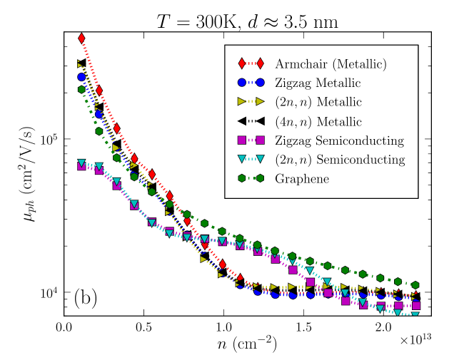
III.2.2 Mobility versus carrier density
We discuss now the evolution of the carrier mobility as a function of , the other parameters ( K, nm) being kept constant (Fig. 2b). For carrier densities of the order of cm-2, the mobilities of the different types of CNTs span more than one order of magnitude. Two trends can be highlighted when is increased. First, the mobility decreases, almost exactly like as in the case of graphene (see the plot of versus in Appendix D). The well-known independence of (or the resistivity) on the Fermi energy or equivalently on the carrier density in graphene at 300 K Hwang08 ; Efetov10 is approximately recovered in CNTs at high carrier density. Second, above cm-2, the mobilities of CNTs and graphene tend to converge to the same value. In that case, the integration over many subbands smooths out the effects resulting from the 1D character of the CNTs. For of the order of cm-2, the mobility is higher in metallic CNTs than in graphene but the situation is reversed when reaches a certain threshold (for example cm-2 for armchair CNTs). In fact, the mobility becomes smaller in metallic CNTs than in graphene when the parabolic subbands start to be occupied (Appendix C). The opposite situation arises when the Fermi level only crosses the linear bands.
III.2.3 Mobility versus temperature
The variations of the mobility with temperature at fixed carrier density ( cm-2) and diameter (3.5 nm) are plotted in Fig. 2c. At high temperature, the mobility in CNTs decreases roughly like where the exponent is close to unity like in graphene but slightly differs from case to case. However, for this particular diameter and carrier density, the spread of the calculated mobilities is still important at 500 K. This shows that the broadening and the averaging induced by the temperature are not sufficient to smooth out 1D band structure effects at this diameter. As already discussed for graphene, the exponent differs from unity because of the increasing role of optical phonons at high temperature. However, we show in the next section that the relative importance of optical phonons at high strongly varies from one CNT to another, being huge in armchair metallic CNTs and remaining modest in semiconducting CNTs [zigzag or ].
III.2.4 Role of the different phonons
In this section, we clarify the relative importance of the different phonons for each type of CNTs, and we compare with the case of graphene.
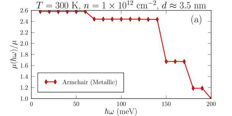
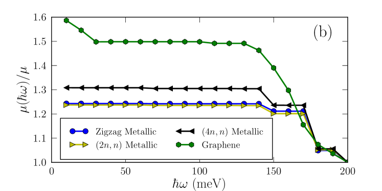
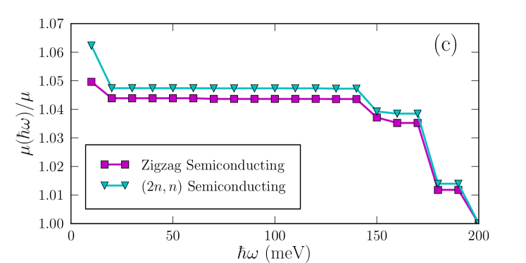
Figure 3 shows the ratio between the mobility calculated by considering phonons with energy up to and the mobility including all phonons. In graphene, this ratio has a plateau around 1.5 from to meV (green line on Fig. 3b). This is consistent with previous studies,Park14 which reported that high-energy phonons contribute to of the resistivity in graphene at room temperature. Similar plateaus are found in CNTs but at different values: 2.5 for armchair CNTs, 1.25 for other metallic CNTs, and 1.05 for semiconducting CNTs ( nm). This means that the relative impact of high energy phonons strongly depends on the type of CNT. In armchair CNTs, this impact is huge – about of the resistivity – because the coupling to LA phonons is forbidden in the linear bands and therefore the relative contribution of the optical phonons is more important. The latter is about in other metallic CNTs, and about in semiconducting CNTs, since the coupling to acoustic phonons is typically strong in parabolic bands.
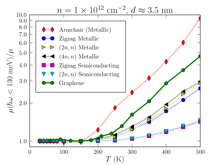
Figure 4 shows that 33% of the electrical resistivity of graphene at 300 K comes from the scattering by high-energy ( meV) phonons, in agreement with recent ab-initio calculations.Park14 This ratio reaches 60% in 3.5 nm armchair metallic CNTs where the coupling to the LA phonons is weak. On the contrary, this ratio is only 5% in 3.5 nm semiconducting CNTs because the scattering by low-energy acoustic phonons is very strong and the mobility is low. The coupling to optical phonons also plays an important role in high-field transport in graphene and CNTs.Yao00 ; Lazzeri05 The impact of high-energy phonons increases with the temperature (Fig. 4). The contribution of these phonons to the resistivity reaches 10% at about , , and K in armchair CNTs, graphene, metallic CNTs and semiconducting CNTs, respectively.
III.2.5 Mobility from CNTs to graphene
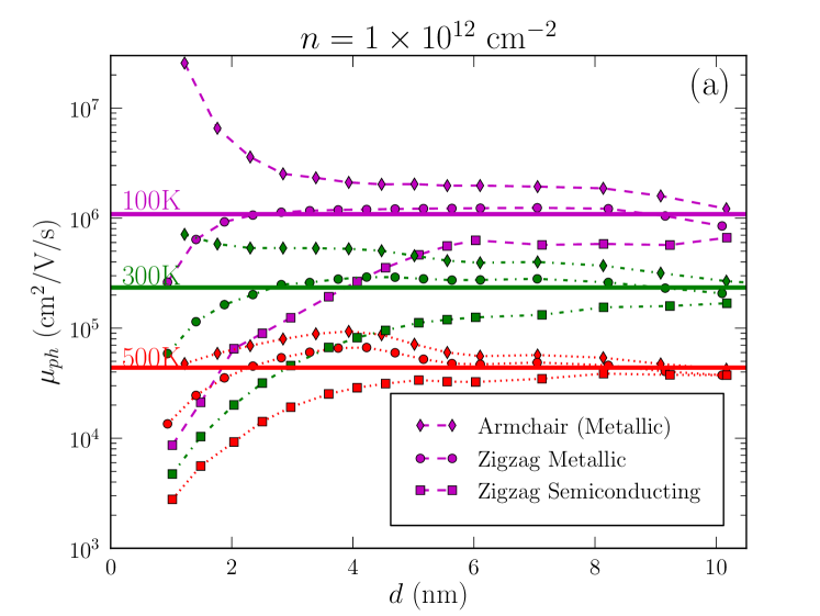
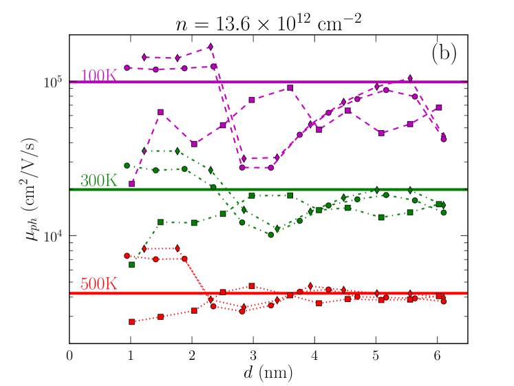
Figure 5 illustrates differently how the mobility in CNTs converges towards the value in graphene when the diameter is increased. The convergence is quite fast at high carrier density ( cm-2) and high temperature ( K, Fig. 5b). For example, at 500 K, the mobility is basically the same in the three kinds of investigated CNTs as in graphene for nm. The transition from 1D to 2D transport takes place above a certain diameter which strongly depends on temperature and carrier density. Below this threshold, the transport properties strongly depend on the chirality through its effect on the band structure.
IV Perspectives
Experimentally, the diameter of single-walled CNTs which are usually grown is typically between 0.7 and 4 nm. However, a recent work reported the synthesis of single-walled CNTs in the 5–10 nm diameter range (5% of the CNTs even have a diameter above 10 nm).Han12 Therefore we believe that the experimental observation of the 1D-2D transition is possible, in particular using the same approach allowing to reach ultrahigh carrier densities up to cm-2 in graphene.Efetov10
Another interesting perspective of the present work would be to consider the effects of electron-electron interactions on the 1D-2D transition in CNTs. As discussed above, the transport properties in graphene at high carrier density and temperature ( K) are unambiguously dominated by electron-phonon scattering. However, theoretical Egger97 ; Kane97 and experimental Bockrath99 studies show that small-diameter metallic CNTs exhibit Luttinger-liquid behaviour characterized by low-energy collective excitations of the electrons. In that case, the tunneling of carriers at energies near the Fermi level is strongly suppressed, so that the conductance increases as a power law with respect to temperature.Bockrath99 On the contrary, the conductance in semiconducting CNTs strongly decreases with temperature, as expected for diffusive transport limited by phonons.Zhou05 All these works deal with small-diameter CNTs at low carrier density. Therefore it would be extremely interesting to extend experimental studies on CNTs to larger diameter and higher carrier density. The electron-phonon interactions should indeed overcome electron-electron interactions when the number of populated subbands increases, in particular for parabolic bands. In these conditions, the carrier mobility in metallic CNTs should follow our predictions above certain thresholds that must be found.
V Conclusion
It is shown that the phonon-limited mobility in 1D CNTs approaches that of 2D graphene continuously by increasing the size of CNTs, the carrier density, or the temperature. The physics of this transition has been studied using atomistic calculations combining a tight-binding model for electrons, a force-constant model for phonons, the computation of all the electron-phonon couplings, and a full resolution of the Boltzmann transport equation. This approach gives carrier mobility in graphene in excellent agreement with experiments Efetov10 and DFT calculations,Park14 and therefore can be used to predict the mobility in CNTs in a wide range of configurations. The mobility in CNTs can be higher or smaller than in graphene depending on chirality, diameter, carrier density or temperature but converges to the same value above varying thresholds. This 1D to 2D transition takes place when the number of subbands situated in the transport energy window is sufficiently large to smooth out the effect of the 1D confinement on the band structure and on the electron-phonon coupling.
Appendix A Parameters for the 4NN force constant model
We have refitted the force constant method of Ref. Wirtz04, to an ab-initio calculation of the phonon-dispersion of graphene using the ABINIT code.Gonze09 The electronic structure is calculated in the local-density approximation (LDA) using a regular 60x60 reciprocal mesh in the first Brillouin zone and an energy cut-off of 35 Ha using a LDA functional. A thermal Fermi-Dirac smearing of 0.002 Ha is employed. We find the optimized cell parameter to be 4.631 Å. The dynamical matrices were calculated using density functional perturbation theory (DFPT) on a 30x30 q-mesh. Since LDA overbinds, i.e., phonon frequencies have the tendency to be slightly too high, a scaling factor is used such that the phonon frequencies of the LO/TO mode at Gamma match the experimental value.Wirtz04
The (real-space) force constants between two particular atoms and are defined as the second derivatives of the total energy of the system with respect to the displacements of atom in direction and of atom in direction :
| (7) |
In local coordinates, direction is along the line connecting the two atoms, is perpendicular to this line in the plane of the graphene sheet, is the out-of-plane direction. In this local reference frame we define the longitudinal forces, (), transverse in-plane (), and transverse-out-of-plane () forces that act on a particular atom when its th nearest-neighbor is displaced. In the conventional 4NN-force constant model, only these “diagonal” terms are fitted. In our model, we include also the “off-diagonal” coupling between the longitudinal direction and the transverse-in-plane direction ( and ). The force-constant matrix for the interaction between two atoms in the local reference frame thus reads:
| (8) |
The off-diagonal force constants and obey the following relations:Dubay
| (9) |
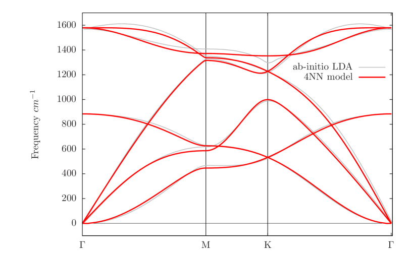
During the fitting, we have noticed that the off-diagonal terms of the second and the fourth nearest neighbor ( and ) are essential. While a fairly decent fit of the phonon-dispersion alone can be achieved without these off-diagonal terms, the correct ratio of the amplitudes of optical and acoustic phonon components in the transverse and longitudinal acoustic branches at can only be achieved with the inclusion of the off-diagonal forces. By using the parameters in Table 1, the ab-initio ratio was reproduced to a very good degree. The comparison of the phonon dispersion relations between the ab-initio calculation and the 4NN force constant model is shown in Fig. 6. We note that the agreement is good but the 4NN model cannot reproduce the Kohn anomalies in the two highest-optical branches. This would require the inclusion of many more distant neighbor interactions in the model (even infinitely many, if one wants to reproduce the kinkDubay ). However, this does not seem to be necessary for our present study since the 4NN model gives electron-phonon scattering rates and carrier mobilities in excellent agreement with ab-initio calculations for graphene.Park14
| n | 1 | 2 | 3 | 4 |
|---|---|---|---|---|
| ( dyn/cm) | 40.905 | 7.402 | -1.643 | -0.609 |
| ( dyn/cm) | 16.685 | -4.051 | 3.267 | 0.424 |
| ( dyn/cm) | 9.616 | -0.841 | 0.603 | -0.501 |
| ( dyn/cm) | 0.000 | 0.632 | 0.000 | -1.092 |
| ( dyn/cm) | 0.000 | -0.632 | 0.000 | -1.092 |
Appendix B Resistivity of graphene including surface optical phonon scattering
The resistivity of graphene was measured in Ref. Zou10, for carrier densities varying from to cm-2. In the following, we show that this resistivity consists of three major components:
| (10) |
where is temperature, is due to impurities, is due to the intrinsic phonons of graphene, and is due to the surface optical phonons of the substrate. is calculated as described in the main document. is calculated with the model of Ref. Konar10, in which SiO2 is considered for the substrate. is determined by taking the difference between experimental data and the sum of and at K. Figure 7 compares the results of the calculation with experimental data Zou10 in a wide range of temperature and for different electron densities . It is clear that they agree very well with each other.
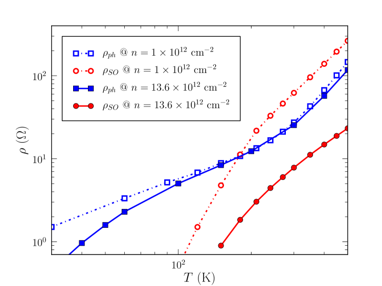
Figure 8 shows the temperature dependence of and . At low temperature, the effect of the surface optical phonon scattering is not significant because the lowest surface optical phonon energy considered in the model is meV. The surface optical phonon scattering is important at high temperature when the carrier density is low. It almost dominates the resistivity at cm-2. However, at higher densities, its contribution becomes negligible due to strong screening.Konar10
Appendix C Band structures of CNTs
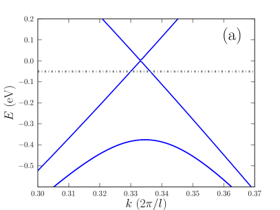
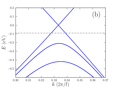

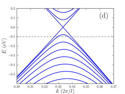
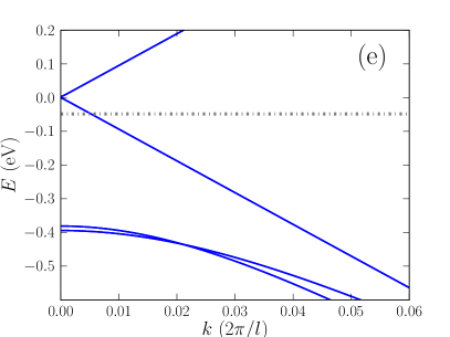
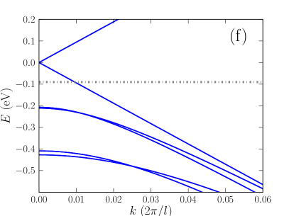
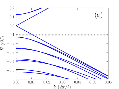
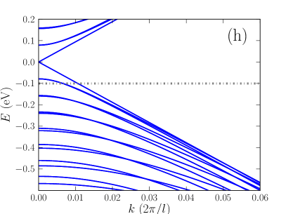

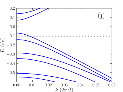
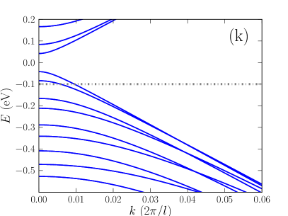
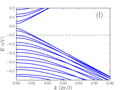
Figure 9 shows the band structure of metallic armchair, metallic zigzag and semiconducting zigzag CNTs for selected diameters. For small diameter CNTs, only the lowest band is involved in the transport. The effective mass of semiconducting CNTs decreases with increasing diameter, leading to higher mobility in CNTs with large diameter.
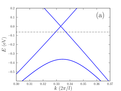

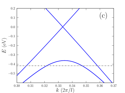
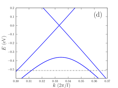
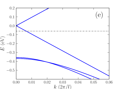
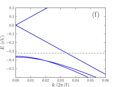
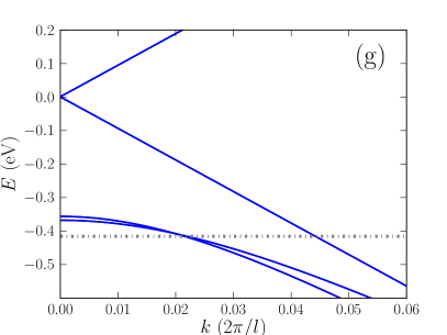

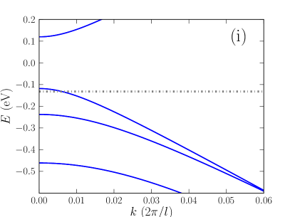
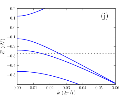
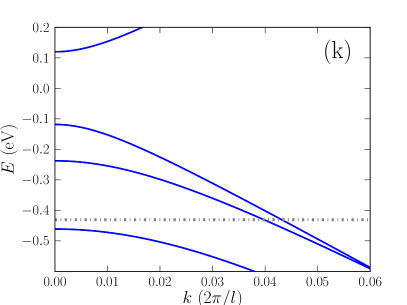
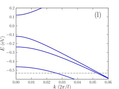
Figure 10 shows the position of the Fermi level in the band structure of CNTs with diameter of nm. This figure helps to interpret the results presented in Fig. 2b. At high carrier density, more bands are included in the transport energy window. That not only brings in bands with finite effective mass, but also more scattering mechanisms.
Appendix D Carrier density dependence of
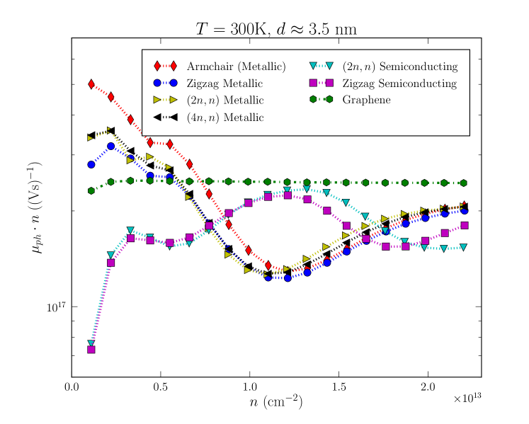
Figure 11 shows that, at 300 K, the product does not depend on the carrier density in graphene. The same behavior is found for CNTs at high carrier density but only approximately, there are deviations coming from band structure effects.
Acknowledgements.
This work was supported by the French National Research Agency (ANR) projects Quasanova (contract ANR-10-NANO-011-02) and Noodles (contract ANR-13-NANO-0009-02). Part of the calculations were run on the TGCC/Curie machine using allocations from GENCI and PRACE. H.M. and L.W. acknowledge support by the National Research Fund (FNR), Luxembourg (projects OTPMD and NanoTMD).References
- (1) R. Saito, G. Dresselhaus, and M. S. Dresselhaus, Physical Properties of Carbon Nanotubes (World Scientific Publishing, 1998)
- (2) J.-C. Charlier, X. Blase, and S. Roche, Rev. Mod. Phys. 79, 677 (May 2007), http://link.aps.org/doi/10.1103/RevModPhys.79.677
- (3) A. Jorio, G. Dresselhaus, and M. Dresselhaus, Carbon Nanotubes: Advanced Topics in the Synthesis, Structure, Properties and Applications, Topics in Applied Physics (Springer Berlin Heidelberg, 2007) ISBN 9783540728658, https://books.google.fr/books?id=ammoVEI-H2gC
- (4) A. H. Castro Neto, F. Guinea, N. M. R. Peres, K. S. Novoselov, and A. K. Geim, Rev. Mod. Phys. 81, 109 (2009), http://link.aps.org/abstract/RMP/v81/p109
- (5) S. V. Morozov, K. S. Novoselov, M. I. Katsnelson, F. Schedin, D. C. Elias, J. A. Jaszczak, and A. K. Geim, Phys. Rev. Lett. 100, 016602 (Jan 2008), http://link.aps.org/doi/10.1103/PhysRevLett.100.016602
- (6) K. I. Bolotin, K. J. Sikes, J. Hone, H. L. Stormer, and P. Kim, Phys. Rev. Lett. 101, 096802 (Aug 2008), http://link.aps.org/doi/10.1103/PhysRevLett.101.096802
- (7) X. Zhou, J.-Y. Park, S. Huang, J. Liu, and P. L. McEuen, Phys. Rev. Lett. 95, 146805 (Sep 2005), http://link.aps.org/doi/10.1103/PhysRevLett.95.146805
- (8) X. Ho, L. Ye, S. V. Rotkin, Q. Cao, S. Unarunotai, S. Salamat, M. A. Alam, and J. A. Rogers, Nano Lett. 10, 499 (2010), http://pubs.acs.org/doi/abs/10.1021/nl903281v
- (9) C. Biswas and Y. H. Lee, Adv. Funct. Mater. 21, 3806 (2011), ISSN 1616-3028, http://dx.doi.org/10.1002/adfm.201101241
- (10) L. M. Woods and G. D. Mahan, Phys. Rev. B 61, 10651 (Apr 2000), http://link.aps.org/doi/10.1103/PhysRevB.61.10651
- (11) H. Suzuura and T. Ando, Phys. Rev. B 65, 235412 (May 2002), http://link.aps.org/doi/10.1103/PhysRevB.65.235412
- (12) J. Jiang, R. Saito, G. G. Samsonidze, S. G. Chou, A. Jorio, G. Dresselhaus, and M. S. Dresselhaus, Phys. Rev. B 72, 235408 (Dec 2005), http://link.aps.org/doi/10.1103/PhysRevB.72.235408
- (13) M. Machón, S. Reich, and C. Thomsen, Phys. Status Solidi (b) 243, 3166 (2006), ISSN 1521-3951, http://dx.doi.org/10.1002/pssb.200669149
- (14) A. C. Ferrari, Solid State Commun. 143, 47 (2007), http://www.sciencedirect.com/science/article/pii/S0038109807002967
- (15) T. Stauber, N. M. R. Peres, and F. Guinea, Phys. Rev. B 76, 205423 (Nov 2007), http://link.aps.org/doi/10.1103/PhysRevB.76.205423
- (16) H. Suzuura and T. Ando, J. Phys. Soc. Jpn. 77, 044703 (2008), http://dx.doi.org/10.1143/JPSJ.77.044703
- (17) E. H. Hwang and S. Das Sarma, Phys. Rev. B 77, 115449 (Mar 2008), http://link.aps.org/doi/10.1103/PhysRevB.77.115449
- (18) E. V. Castro, H. Ochoa, M. I. Katsnelson, R. V. Gorbachev, D. C. Elias, K. S. Novoselov, A. K. Geim, and F. Guinea, Phys. Rev. Lett. 105, 266601 (Dec 2010), http://link.aps.org/doi/10.1103/PhysRevLett.105.266601
- (19) V. Perebeinos and P. Avouris, Phys. Rev. B 81, 195442 (May 2010), http://link.aps.org/doi/10.1103/PhysRevB.81.195442
- (20) K. M. Borysenko, J. T. Mullen, E. A. Barry, S. Paul, Y. G. Semenov, J. M. Zavada, M. B. Nardelli, and K. W. Kim, Phys. Rev. B 81, 121412 (Mar 2010), http://link.aps.org/doi/10.1103/PhysRevB.81.121412
- (21) C. Attaccalite, L. Wirtz, M. Lazzeri, F. Mauri, and A. Rubio, Nano Lett. 10, 1172 (2010)
- (22) K. Kaasbjerg, K. S. Thygesen, and K. W. Jacobsen, Phys. Rev. B 85, 165440 (Apr 2012), http://link.aps.org/doi/10.1103/PhysRevB.85.165440
- (23) C.-H. Park, N. Bonini, T. Sohier, G. Samsonidze, B. Kozinsky, M. Calandra, F. Mauri, and N. Marzari, Nano Lett. 14, 1113 (2014), http://pubs.acs.org/doi/abs/10.1021/nl402696q
- (24) D. K. Efetov and P. Kim, Phys. Rev. Lett. 105, 256805 (Dec 2010), http://link.aps.org/doi/10.1103/PhysRevLett.105.256805
- (25) M. Luisier and G. Klimeck, Phys. Rev. B 80, 155430 (Oct 2009)
- (26) W. Zhang, C. Delerue, Y.-M. Niquet, G. Allan, and E. Wang, Phys. Rev. B 82, 115319 (Sep 2010), http://link.aps.org/doi/10.1103/PhysRevB.82.115319
- (27) N. Neophytou and H. Kosina, Phys. Rev. B 84, 085313 (Aug 2011)
- (28) E. Mariani and F. von Oppen, Phys. Rev. B 82, 195403 (Nov 2010), http://link.aps.org/doi/10.1103/PhysRevB.82.195403
- (29) V. Perebeinos, J. Tersoff, and P. Avouris, Phys. Rev. Lett. 94, 086802 (Mar 2005), http://link.aps.org/doi/10.1103/PhysRevLett.94.086802
- (30) L. E. F. Foa Torres and S. Roche, Phys. Rev. Lett. 97, 076804 (Aug 2006), http://link.aps.org/doi/10.1103/PhysRevLett.97.076804
- (31) V. N. Popov and P. Lambin, Phys. Rev. B 74, 075415 (AUG 2006), ISSN 1098-0121
- (32) M. Z. Kauser and P. P. Ruden, J. Appl. Phys. 102, 033712 (2007), http://scitation.aip.org/content/aip/journal/jap/102/3/10.1063/1.276722%4
- (33) G. Pennington, N. Goldsman, A. Akturk, and A. E. Wickenden, Appl. Phys. Lett. 90, 062110 (FEB 5 2007)
- (34) S. O. Koswatta, S. Hasan, M. S. Lundstrom, M. P. Anantram, and D. E. Nikonov, IEEE Trans. Electron. Dev. 54, 2339 (SEP 2007), ISSN 0018-9383
- (35) Y. Zhao, A. Liao, and E. Pop, Electron Device Lett. 30, 1078 (Oct 2009), ISSN 0741-3106
- (36) T. Sohier, M. Calandra, C.-H. Park, N. Bonini, N. Marzari, and F. Mauri, Phys. Rev. B 90, 125414 (Sep 2014), http://link.aps.org/doi/10.1103/PhysRevB.90.125414
- (37) K. Zou, X. Hong, D. Keefer, and J. Zhu, Phys. Rev. Lett. 105, 126601 (Sep 2010), http://link.aps.org/doi/10.1103/PhysRevLett.105.126601
- (38) W. Harrison, Electronic structure and the properties of solids: the physics of the chemical bond, Dover Books on Physics (Dover Publications, 1989) ISBN 9780486660219, http://books.google.fr/books?id=orAPAQAAMAAJ
- (39) Y. M. Niquet, D. Rideau, C. Tavernier, H. Jaouen, and X. Blase, Phys. Rev. B 79, 245201 (Jun 2009), http://link.aps.org/doi/10.1103/PhysRevB.79.245201
- (40) L. Genovese, A. Neelov, S. Goedecker, T. Deutsch, S. A. Ghasemi, A. Willand, D. Caliste, O. Zilberberg, M. Rayson, A. Bergman, and R. Schneider, J. Chem. Phys. 129, 014109 (2008), http://scitation.aip.org/content/aip/journal/jcp/129/1/10.1063/1.294954%7
- (41) M. Krack, Theor. Chem. Acc. 114, 145 (2005), ISSN 1432-881X, http://dx.doi.org/10.1007/s00214-005-0655-y
- (42) J. P. Perdew, K. Burke, and M. Ernzerhof, Phys. Rev. Lett. 77, 3865 (Oct 1996), http://link.aps.org/doi/10.1103/PhysRevLett.77.3865
- (43) L. Genovese, T. Deutsch, and S. Goedecker, J. Chem. Phys. 127, 054704 (2007), http://scitation.aip.org/content/aip/journal/jcp/127/5/10.1063/1.275468%5
- (44) The computation was set up to guarantee an accuracy of at least 0.5 meV for the Kohn-Sham eigenvalues. This corresponds to a uniform wavelet grid with a spacing of 0.3 bohrs, and a Monkhorst-Pack mesh of 362 k-points, for a non-irreductible supercell of 4 carbon atoms. We took care to include explicitly the Dirac point in the Brilloiun zone sampling.
- (45) M. Dresselhaus, G. Dresselhaus, R. Saito, and A. Jorio, Phys. Rep. 409, 47 (2005), ISSN 0370-1573, http://www.sciencedirect.com/science/article/pii/S0370157304004570
- (46) C. L. Kane and E. J. Mele, Phys. Rev. Lett. 78, 1932 (Mar 1997), http://link.aps.org/doi/10.1103/PhysRevLett.78.1932
- (47) M. Ouyang, J.-L. Huang, C. L. Cheung, and C. M. Lieber, Science 292, 702 (2001), http://www.sciencemag.org/content/292/5517/702.abstract
- (48) X. Blase, L. X. Benedict, E. L. Shirley, and S. G. Louie, Phys. Rev. Lett. 72, 1878 (Mar 1994), http://link.aps.org/doi/10.1103/PhysRevLett.72.1878
- (49) R. A. Jishi, R. M. Mirie, M. S. Dresselhaus, G. Dresselhaus, and P. C. Eklund, Phys. Rev. B 48, 5634 (Aug 1993), http://link.aps.org/doi/10.1103/PhysRevB.48.5634
- (50) L. Wirtz and A. Rubio, Solid State Comm. 131, 141 (2004), ISSN 0038-1098, http://www.sciencedirect.com/science/article/pii/S0038109804003424
- (51) O. Dubay and G. Kresse, Phys. Rev. B 67, 035401 (Jan 2003), http://link.aps.org/doi/10.1103/PhysRevB.67.035401
- (52) J.-Y. Park, S. Rosenblatt, Y. Yaish, V. Sazonova, H. Üstünel, S. Braig, T. A. Arias, P. W. Brouwer, and P. L. McEuen, Nano Lett. 4, 517 (2004), http://pubs.acs.org/doi/abs/10.1021/nl035258c
- (53) Z. Yao, C. L. Kane, and C. Dekker, Phys. Rev. Lett. 84, 2941 (Mar 2000), http://link.aps.org/doi/10.1103/PhysRevLett.84.2941
- (54) M. Lazzeri, S. Piscanec, F. Mauri, A. C. Ferrari, and J. Robertson, Phys. Rev. Lett. 95, 236802 (Nov 2005), http://link.aps.org/doi/10.1103/PhysRevLett.95.236802
- (55) Z. J. Han and K. K. Ostrikov, J. Am. Chem. Soc. 134, 6018 (2012), http://pubs.acs.org/doi/abs/10.1021/ja300805s
- (56) R. Egger and A. O. Gogolin, Phys. Rev. Lett. 79, 5082 (Dec 1997), http://link.aps.org/doi/10.1103/PhysRevLett.79.5082
- (57) C. Kane, L. Balents, and M. P. A. Fisher, Phys. Rev. Lett. 79, 5086 (Dec 1997), http://link.aps.org/doi/10.1103/PhysRevLett.79.5086
- (58) M. Bockrath, D. Cobden, J. Lu, A. Rinzler, R. Smalley, L. Balents, and P. McEuen, Nature 397, 598 (FEB 18 1999)
- (59) X. Gonze, B. Amadon, P.-M. Anglade, J.-M. Beuken, F. Bottin, P. Boulanger, F. Bruneval, D. Caliste, R. Caracas, M. Côté, T. Deutsch, L. Genovese, P. Ghosez, M. Giantomassi, S. Goedecker, D. Hamann, P. Hermet, F. Jollet, G. Jomard, S. Leroux, M. Mancini, S. Mazevet, M. Oliveira, G. Onida, Y. Pouillon, T. Rangel, G.-M. Rignanese, D. Sangalli, R. Shaltaf, M. Torrent, M. Verstraete, G. Zerah, and J. Zwanziger, Comput. Phys. Commun. 180, 2582 (2009), http://www.sciencedirect.com/science/article/pii/S0010465509002276
- (60) A. Konar, T. Fang, and D. Jena, Phys. Rev. B 82, 115452 (Sep 2010), http://link.aps.org/doi/10.1103/PhysRevB.82.115452