First-principles Simulations of a Graphene Based Field-Effect Transistor
Abstract
We improvise a novel approach to carry out first-principles simulations of graphene-based vertical field effect tunneling transistors that consist of a grapheneh-BNgraphene multilayer structure. Within the density functional theory framework, we exploit the effective screening medium (ESM) method to properly treat boundary conditions for electrostatic potentials and investigate the effect of gate voltage. The distribution of free carriers and the band structure of both top and bottom graphene layers are calculated self-consistently. The dielectric properties of h-BN thin films sandwiched between graphene layers are computed layer-by-layer following the theory of microscopic permittivity. We find that the permittivities of BN layers are very close to that of crystalline h-BN. The effect of interface with graphene on the dielectric properties of h-BN is weak, according to an analysis on the interface charge redistribution.
I introduction
Graphene-based field-effect transistors have been synthesized,Novoselov et al. (2004) but the ratio of high and low resistances (switching ratio) is limited (less than a factor of ) because of the zero-gap band structure of pristine graphene. A possible solution is to introduce an energy gap into graphene by using, for instance, bilayer graphene,Castro et al. (2007); Oostinga et al. (2007) nanoribbons,Han et al. (2007) or chemical derivatives.Elias et al. (2009) Recently, Britnell et al.Britnell et al. (2012); Georgiou et al. (2013); Britnell et al. (2013) reported an alternative transistor architecture, a vertical field effect tunneling transistor (FETT), exhibiting a fairly high () switching ratio. In FETT devices, a graphenebarriergraphene trilayer is utilized as the current-carrying channel, as in Fig. 1(a); the electric current flows into the channel through one graphene layer and out through the other. Inside the trilayer, electrons cross the thin barrier via tunneling. The chemical potentials of the two graphene layers and the tunneling conductance can be tuned by gate voltages. The bottom graphene layer (closer to gate electrode, ) can only partially screen the gate voltage because of the low density of states (DOS) near the Dirac point, and so the top graphene layer (away from gate electrode, ) is also affected by the gate voltage.
In a typical field-effect device, the current-carrying channel is separated by a thick dielectric from a metallic gate electrode. A gate voltage applied between the gate electrode and the current-carrying channel controls the free carrier density in the channel. The spatial distribution of free carriers can be obtained by solving the electrostatic Poisson equation. Macroscopic physical quantities of device components are used as parameters for Poisson’s equation, including dielectric constants and electron affinities of dielectrics and work functions of gate electrodes, etc. Luo et al. (2007) However, the extrapolation of the macroscopic theory of electrostatics to the nanometer scale is unjustified, because interfaces often exhibit dielectric screening properties different from the bulk.Jackson (1998) The applicability of the macroscopic theory should be examined by studying the materials-specific dielectric screening properties of interfaces, one of motivations of this work. The density functional theory (DFT) method fully takes the atomic structure of a device into account, and microscopic electrostatics quantities such as potential and charge density can be solved self-consistently, from which microscopic dielectric properties can be deduced.Giustino et al. (2003) One can extract an effective dielectric constant from microscopic calculations to represent the dielectric screening of the interface, which is not necessarily a constant but a quantity that depends on the thickness of the interface and other factors.
The boundary condition is crucial in solving for the electrostatic potential. In an FET device, for example, the electrostatic potential at the surface of a metallic gate electrode should be constant, and the electric field (derivative of the potential) in vacuum far away from the device should be zero. This mixed boundary condition is different from the conventional and widely-implemented periodic boundary condition. Otani et al.Otani and Sugino (2006) proposed a Green’s-function-based effective screening medium (ESM) approach to solve the electrostatic potential under several different boundary conditions, which is promising for simulating the electric-field effect in planar devices.
In this work, graphene-based FETT devices were simulated using a DFT+ESM method. The computational approach, based on first principles, enables us to understand interface effects quantitatively, and thus enables computational design of functional systems. The rest of the paper is organized as follows. In the next Section, details of the computational method are presented. The distribution of free carriers and the band structures of graphene layers under different gate voltages are presented in Sec. III. The effective dielectric constant of the h-BN thin barrier in FETT is analyzed in Sec. IV. Finally, we give a summary on our results in Sec. V.
II simulation method
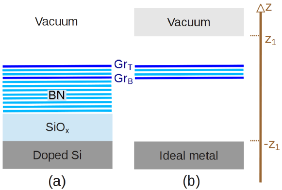
The structure of the FETT used in experimentsBritnell et al. (2012) is schematically shown in Fig. 1(a). Doped silicon is used as the gate electrode, which is separated from the current-carrying h-BN trilayer channel by insulating silicon oxide () and h-BN thin films (). The gate voltage is applied between the doped silicon and the trilayer.
In our DFT simulations, the doped silicon gate electrode was replaced by a semi-infinite ideally metallic medium for [Fig. 1(b); the -direction is perpendicular to the h-BN trilayer], and the dielectrics between the gate electrode and the h-BN trilayer were replaced by vacuum to save computational resources. Thus the h-BN trilayer is sandwiched by a semi-infinite vacuum medium () and an ideally metallic medium (), see Fig. 1(b). Note that the semi-infinite vacuum and metallic media are not explicitly included in calculations, instead they are used as boundary conditions for the Hartree potential (),
| (1) |
We adopted the ESM methodOtani and Sugino (2006) to solve the Hartree potential. The purpose to employ this method is twofold: (i) Long-range Coulomb interactions with periodic images are avoided. (ii) The non-periodic boundary condition of Eq. (1) for the Hartree potential can be imposed.
A gate voltage can be simulated by adding extra electrons or holes to the h-BN trilayer;Otani and Sugino (2006) the areal density of free carriers is proportional to the gate voltage. In experiments the carrier density in graphene can be tuned by gate voltage up to , which is equivalent to electrons per primitive unit cell of graphene, or an electric displacement field of in the dielectrics.
The measured interlayer distance between h-BN and graphene layersHaigh et al. (2012) is , and the interlayer distance between h-BN layers is taken as half of the lattice constant of crystalline h-BN.Levinshtein et al. (2001) In-plane lattice constants for both graphene and h-BN were set to due to the small lattice mismatch between them. In the - plane a periodic boundary condition was applied with a dense Monkhorst-PackMonkhorst and Pack (1976) -mesh. The cutoff energy for wave functions and the Methfessel-PaxtonMethfessel and Paxton (1989) spreading energy were taken to be and , respectively. The Perdew-Burke-Ernzerhof parameterizationPerdew et al. (1996) of the generalized gradient approximation (GGA) to the exchange-correlation functional and Trouiller-Martins norm-conserving pseudopotentials were used. DFT calculations were performed using the Quantum ESPRESSO packageGiannozzi et al. (2009).
Charge density in the h-BN trilayer was calculated self-consistently for different gate voltages. In order to illustrate the distribution of free carriers across the trilayer, it is convenient to integrate the charge density in the - plane and define a charge density along -direction . The density of free carriers is defined as charge density difference for a device under a finite gate voltage with respect to that under zero gate voltage. Compared to gate voltages, the electric displacement field in the dielectrics is a more convenient quantity, because it is independent of the thickness or the dielectric constant of the dielectrics. Gate voltages are expressed as hereafter.
III results
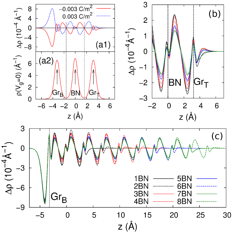
A FETT with a monolayer h-BN barrier is used as an example to illustrate the charge and free carrier densities in such devices.. The charge and free carrier density on each layer can be analyzed using the Bader decomposition,Bader (1990) in which boundaries between atoms are defined by zero flux surfaces. There are three peaks in the charge density curve , corresponding to the , h-BN, and layers, respectively; cf. Fig. 2(a2). Free carrier densities , defined as the change in charge density induced by gate voltages, under are shown in Fig. 2(a1), where it can be seen that they have opposite sign but almost the same amplitude, in accordance with the electron-hole symmetry of graphene in the vicinity of the Fermi energy. For the one-dimensional charge density , atomic layers are divided by minima of , as denoted by vertical dashed lines in Fig. 2(a2) (zero flux surfaces shrink to points for the one-dimensional charge density.) A large portion of the free carriers accumulate on at the side closer to the gate electrode; thus the free carrier density on is larger than that on . The asymmetric shape of with respect to the central h-BN layer is a consequence of the asymmetric environment of the h-BN trilayer, with the metallic gate electrode on one side and vacuum on the other side.
The h-BN barrier can screen the applied gate voltage by developing an internal electric polarization, which reduces the effect of the gate voltage and the free carrier density in . We performed calculations on devices with a h-BN barrier thickness of up to eight monolayers. The free carrier density for these devices as a function of for is shown in Figs. 2(b) and 2(c), shifted to make the positions of the (b) or (c) layers coincide. The distribution of free carriers on is almost independent of the thickness of the h-BN barrier, cf. Fig. 2(c). The amplitude of the electric polarization in the h-BN barrier shrinks for thicker barriers (Fig. 2(c)), and so does the free carrier density in (Fig. 2(b)), indicating that thicker h-BN barriers provide stronger screening.
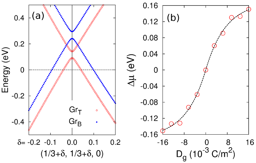
The chemical potential of graphene, defined as the energy difference between the Fermi energy and the charge neutrality point, can be efficiently tuned by using gate voltages because of the small DOS near the Fermi energy.Britnell et al. (2012); Georgiou et al. (2013); Britnell et al. (2013) The band structure of a h-BN trilayer in the vicinity of the Fermi energy has contributions only from graphene layers, because h-BN is a wide gap insulator with a calculated energy band gap of . The band structure of graphene shows a tiny energy gap of [Fig. 3(a)] induced by interaction with h-BN.Giovannetti et al. (2007) A FETT with a h-BN barrier thicker than one monolayer shows no hybridization between and in its band structure. As an example, the band structure of a FETT with a five-layer-thick h-BN barrier for is shown in Fig. 3(a), where bands from and shift upward rigidly by and with respect to the Fermi energy, respectively. The bands from are always shifted away from the Fermi level by a larger energy than those from [Fig. 3(b)].
IV discussion
Macroscopic electrostatic models have been used to calculate the electrostatic potential and free carrier density in graphene based FETT. Britnell et al. (2012); Ponomarenko et al. (2013); Kumar et al. (2012); Fiori et al. (2013) In these models, the h-BN barrier between graphene layers is assumed to have a dielectric constant equal to that of the h-BN crystal. However, interfaces can exhibit significantly different dielectric properties compared to the bulk,Giustino et al. (2003) and the dielectric properties of a few-layer-thick h-BN barrier sandwiched between two graphene layers need to be revisited. We seek to find the (effective) dielectric constant of a h-BN barrier in a FETT and compare to its bulk value, in order to investigate if the dielectric constant is still a valid physical concept for thin h-BN films and to investigate whether of a h-BN barrier is modified by the interfaces with graphene layers.
The dielectric constants of h-BN thin films () sandwiched between graphene layers can be deduced from the electric field inside the h-BN thin film () and the electric polarization () induced by gate voltages,
| (2) |
where is equal to the slope of the self-consistent Kohn-Sham effective potential in the -direction. is also related to the difference between chemical potentials of graphene layers by , where is the distance between the two graphene layers.
The polarization can be expressed as the summation of centers of Wannier functions according to the modern theory of polarization. King-Smith and Vanderbilt (1993); Resta (1994) In practice we followed the method proposed in Refs. Stengel and Spaldin, 2007; Stengel et al., 2009 which extends the Wannier function theory of polarization King-Smith and Vanderbilt (1993); Resta (1994); Giustino and Pasquarello (2005); Wu et al. (2006) to metal-insulator heterostructures.
The hybrid Wannier functions Marzari and Vanderbilt (1997); Sgiarovello et al. (2001), which are exponentially localized in the direction but Bloch-like in the - plane, were constructed using the parallel-transport method.Marzari and Vanderbilt (1997); Sgiarovello et al. (2001) The first Brillouin zone was sampled by discrete -points of the type , where the vectors form a uniform mesh in the - plane, and is along the -direction with the height of the unit cell and the number of -points along the -direction. The total number of -points is . We used and , which are sufficient to converge the polarization.
The matrices were constructed where is periodic under lattice translations and is the band index; is normalized such that . Singular value decomposition of each matrix was done utilizing the LAPACK library: where and are complex unitary matrices and is a diagonal matrix with diagonal elements very close to 1 for small . A new matrix was constructed corresponding to each matrix, and a global matrix was then constructed for each point. The centers of hybrid Wannier functions were calculated as , where the are the eigenvalues of .
The number of bands considered to construct the hybrid Wannier functions, i.e., the dimension of the matrices, is equal to four for each graphene or h-BN atomic layer, the number of occupied bands in most of the first Brillouin zone except for the small portion near the -point (see Fig. 3). This choice does not affect the calculations of the polarization inside h-BN thin films because the bands near the Fermi energy are contributed by graphene layers.
Four of the resulting hybrid Wannier functions can be assigned to each graphene or h-BN layer according to the positions of their centers. Two of them are very close to the atomic plane (within ) and the other two are located about above and beneath the atomic plane respectively. The center of charge for each atomic layer is equal to the average value of the corresponding four Wannier functions. The dipole moment corresponding to each h-BN layer was calculated using the shift of the center of charge under an electric field, and the polarization was calculated with the thickness of each h-BN layer set to be .
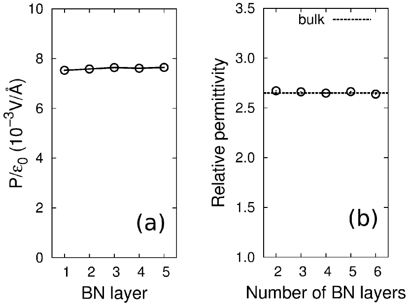
The calculated polarization of the h-BN layer adjacent to the graphene layers is almost the same as h-BN layers deeply inside [see Fig. 4(a)], indicating that interface with graphene layers has little effect on the dielectric properties of h-BN thin films. As a result, the average dielectric constant for h-BN thin films embedded by graphene layers is independent of the thickness; see Fig. 4(b).
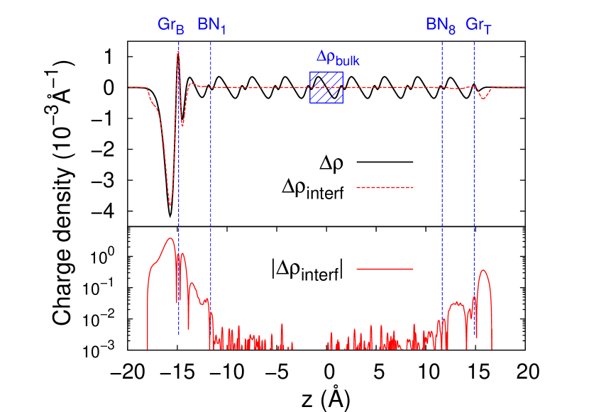
The effect of an interface with graphene on the dielectric properties of h-BN can be analyzed using the interface charge redistribution, denoted as and defined as the difference in charge redistribution at the interface with respect to that in the bulk (denoted as ). In practice we used the charge redistribution at the center of the h-BN as the bulk, as shown in Fig. 5. Thus one can obtain by subtracting from the total charge redistribution. Because h-BN is a wide-band-gap insulator, should decay exponentially away from the interface. The strength of the interface effect is determined by the amplitude of near the interface.
An example the charge redistribution in a FETT device with eight-layer h-BN for is shown in Fig. 5. The difference is large near the graphene layers, decays quickly into h-BN, and becomes invisible after crossing the first h-BN atomic layers ( and in Fig. 5). The amplitude of is also presented on a logarithmic scale in the lower panel of Fig. 5. The decay of into h-BN is approximately exponential. Most importantly, the amplitude of is about times smaller than that of between and in Fig. 5: is very small inside the atomic plane of the first h-BN layer. As a result, any interface effect on the dielectric properties of h-BN is very weak, which explains why the calculated dielectric constant of h-BN in FETT devices is close to the bulk value.
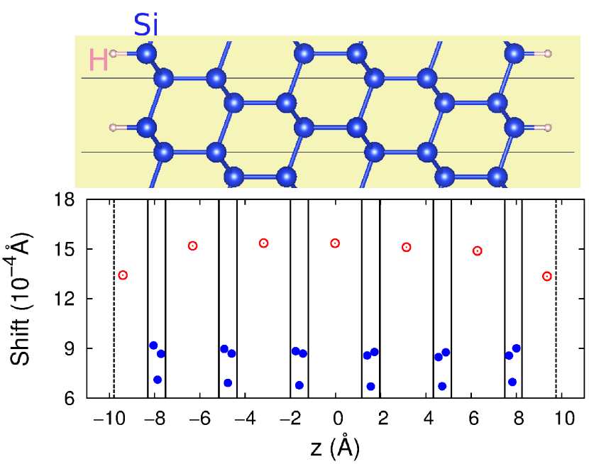
We also compared the h-BN thin films with silicon thin films, because the latter are known to exhibit lower dielectric permittivity than for the corresponding bulk. Giustino et al. (2003); Giustino and Pasquarello (2005) The in-plane lattice constant of Si(111) slabs was chosen to be the experimental lattice constant of fcc-Si. Dangling bonds on both surfaces are saturated by hydrogen, as shown in the upper panel of Fig. 6, and the Si-H bond length is after structure optimization.
We plotted in Fig. 6 the shift of each hybrid Wannier functions induced by an electric field of along the -direction, where the electric field was applied using the ESM method using a metalslabmetal configuration. The hybrid Wannier functions can be divided into two categories according to their polarizability. The hybrid Wannier functions located at canted Si-Si bonds with respect to the -direction (denoted as in Fig. 6) exhibit lower polarizability, and they show negligible deviations at the surface. On the other hand, the hybrid Wannier functions located at parallel Si-Si or Si-H bonds with respect to the -direction (denoted as in Fig. 6) exhibit higher polarizability. We also observed that the hybrid Wannier functions of Si-H bonds at the surface show a polarizability 12% lower than those corresponding to parallel Si-Si bonds. The 12% lower polarizability of the Si(111) surfaces shown in Fig. 6 is not as severe as reported by previous studies.Giustino and Pasquarello (2005); Nakamura et al. (2006) In those studies, the macroscopic polarization and dielectric constant were obtained after a smoothing procedure. The purpose of the smoothing procedure is to eliminate the dielectric nonlocality, but this procedure reduces the dielectric permittivity of surfaces artificially because the dielectric constant of vacuum is smeared into the surface.
V summary
The distribution of free carriers and the band structure of graphene layers in graphene based FETT have been simulated using the DFT+ESM method. The dielectric properties of h-BN thin films sandwiched between graphene layers in FETT were investigated using the theory of microscopic permittivity and found to have a dielectric permittivity close to that of crystalline h-BN. The small amplitude of interface charge redistribution inside the atomic plane of the first h-BN layer proves that the effect of the interface with graphene on the dielectric properties of h-BN is weak.
In this study we have demonstrated the DFT+ESM method as a promising approach to simulate field-effect devices with a planar structure. Once the charge density and effective potential of a field-effect device are self-consistently obtained, the scattering of transport electrons and electric conductivity can be calculated using scattering theory.
Acknowledgements.
This work was supported by the US Department of Energy (DOE), Office of Basic Energy Sciences (BES), under Contract No. DE-FG02-02ER45995. This research used resources of the National Energy Research Scientific Computing Center.References
- Novoselov et al. (2004) K. S. Novoselov, A. K. Geim, S. V. Morozov, D. Jiang, Y. Zhang, S. V. Dubonos, I. V. Grigorieva, and A. A. Firsov, Science 306, 666 (2004).
- Castro et al. (2007) E. V. Castro, K. S. Novoselov, S. V. Morozov, N. M. R. Peres, J. M. B. L. dos Santos, J. Nilsson, F. Guinea, A. K. Geim, and A. H. C. Neto, Phys. Rev. Lett. 99, 216802 (2007).
- Oostinga et al. (2007) J. B. Oostinga, H. B. Heersche, X. Liu, A. F. Morpurgo, and L. M. K. Vandersypen, Nat. Mater. 7, 151 (2007).
- Han et al. (2007) M. Y. Han, B. Özyilmaz, Y. Zhang, and P. Kim, Phys. Rev. Lett. 98, 206805 (2007).
- Elias et al. (2009) D. C. Elias, R. R. Nair, T. M. G. Mohiuddin, S. V. Morozov, P. Blake, M. P. Halsall, A. C. Ferrari, D. W. Boukhvalov, M. I. Katsnelson, A. K. Geim, and K. S. Novoselov, Science 323, 610 (2009).
- Britnell et al. (2012) L. Britnell, R. V. Gorbachev, R. Jalil, B. D. Belle, F. Schedin, A. Mishchenko, T. Georgiou, M. I. Katsnelson, L. Eaves, S. V. Morozov, N. M. R. Peres, J. Leist, A. K. Geim, K. S. Novoselov, and L. A. Ponomarenko, Science 335, 947 (2012).
- Georgiou et al. (2013) T. Georgiou, R. Jalil, B. D. Belle, L. Britnell, R. V. Gorbachev, S. V. Morozov, Y.-J. Kim, A. Gholinia, S. J. Haigh, O. Makarovsky, L. Eaves, L. A. Ponomarenko, A. K. Geim, K. S. Novoselov, and A. Mishchenko, Nature Nanotech. 8, 100 (2013).
- Britnell et al. (2013) L. Britnell, R. V. Gorbachev, A. K. Geim, L. A. Ponomarenko, A. Mishchenko, M. T. Greenaway, T. M. Fromhold, K. S. Novoselov, and L. Eaves, Nature Commun. 4, 1794 (2013).
- Luo et al. (2007) J.-W. Luo, S.-S. Li, J.-B. Xia, and L.-W. Wang, Appl. Phys. Lett. 90, 143108 (2007).
- Jackson (1998) J. D. Jackson, Classical Electrodynamics, 3rd ed. (Wiley, 1998).
- Giustino et al. (2003) F. Giustino, P. Umari, and A. Pasquarello, Phys. Rev. Lett. 91, 267601 (2003).
- Otani and Sugino (2006) M. Otani and O. Sugino, Phys. Rev. B 73, 115407 (2006).
- Haigh et al. (2012) S. J. Haigh, A. Gholinia, R. Jalil, S. Romani, L. Britnell, D. C. Elias, K. S. Novoselov, L. A. Ponomarenko, A. K. Geim, and R. Gorbachev, Nat. Mater. 11, 764 (2012).
- Levinshtein et al. (2001) M. E. Levinshtein, S. L. Rumyantsev, and M. S. Shur, eds., Properties of Advanced Semiconductor Materials: GaN, AIN, InN, BN, SiC, SiGe, 1st ed. (Wiley-Interscience, New York, 2001).
- Monkhorst and Pack (1976) H. J. Monkhorst and J. D. Pack, Phys. Rev. B 13, 5188 (1976).
- Methfessel and Paxton (1989) M. Methfessel and A. T. Paxton, Phys. Rev. B 40, 3616 (1989).
- Perdew et al. (1996) J. P. Perdew, K. Burke, and M. Ernzerhof, Phys. Rev. Lett. 77, 3865 (1996).
- Giannozzi et al. (2009) P. Giannozzi, S. Baroni, N. Bonini, M. Calandra, R. Car, C. Cavazzoni, D. Ceresoli, G. L. Chiarotti, M. Cococcioni, I. Dabo, A. Dal Corso, S. de Gironcoli, S. Fabris, G. Fratesi, R. Gebauer, U. Gerstmann, C. Gougoussis, A. Kokalj, M. Lazzeri, L. Martin-Samos, N. Marzari, F. Mauri, R. Mazzarello, S. Paolini, A. Pasquarello, L. Paulatto, C. Sbraccia, S. Scandolo, G. Sclauzero, A. P. Seitsonen, A. Smogunov, P. Umari, and R. M. Wentzcovitch, J. Phys.: Condens. Matter 21, 395502 (2009).
- Bader (1990) R. F. W. Bader, Atoms in molecules: a quantum theory (Oxford University Press, New York, 1990).
- Giovannetti et al. (2007) G. Giovannetti, P. A. Khomyakov, G. Brocks, P. J. Kelly, and J. van den Brink, Phys. Rev. B 76, 073103 (2007).
- Ponomarenko et al. (2013) L. A. Ponomarenko, B. D. Belle, R. Jalil, L. Britnell, R. V. Gorbachev, A. K. Geim, K. S. Novoselov, A. H. Castro Neto, L. Eaves, and M. I. Katsnelson, J. Appl. Phys. 113, 136502 (2013).
- Kumar et al. (2012) S. B. Kumar, G. Seol, and J. Guo, Appl. Phys. Lett. 101, 033503 (2012).
- Fiori et al. (2013) G. Fiori, S. Bruzzone, and G. Iannaccone, IEEE Trans. Electron. Dev. 60, 268 (2013).
- King-Smith and Vanderbilt (1993) R. D. King-Smith and D. Vanderbilt, Phys. Rev. B 47, 1651 (1993).
- Resta (1994) R. Resta, Rev. Mod. Phys. 66, 899 (1994).
- Stengel and Spaldin (2007) M. Stengel and N. A. Spaldin, Phys. Rev. B 75, 205121 (2007).
- Stengel et al. (2009) M. Stengel, D. Vanderbilt, and N. A. Spaldin, Phys. Rev. B 80, 224110 (2009).
- Giustino and Pasquarello (2005) F. Giustino and A. Pasquarello, Phys. Rev. B 71, 144104 (2005).
- Wu et al. (2006) X. Wu, O. Diéguez, K. M. Rabe, and D. Vanderbilt, Phys. Rev. Lett. 97, 107602 (2006).
- Marzari and Vanderbilt (1997) N. Marzari and D. Vanderbilt, Phys. Rev. B 56, 12847 (1997).
- Sgiarovello et al. (2001) C. Sgiarovello, M. Peressi, and R. Resta, Phys. Rev. B 64, 115202 (2001).
- Nakamura et al. (2006) J. Nakamura, S. Ishihara, and A. Natori, J. Appl. Phys. 99, 054309 (2006).