Dual cut-off dc-tunable microwave low-pass filter on superconducting Nb microstrips with asymmetric nanogrooves
Abstract
We present a dual cut-off, dc-tunable low-pass microwave filter on a superconducting Nb microstrip with uniaxial asymmetric nanogrooves. The frequency response of the device was measured in the range KHz to GHz at different temperatures, magnetic fields, and dc current values. The microwave loss is most effectively reduced when the Abrikosov vortex lattice spatially matches the underlying washboard pinning landscape. The forward transmission coefficient of the microstrip has a dc-tunable cut-off frequency which notably changes under dc bias reversal, due to the two different slope steepnesses of the pinning landscape. The device’s operation principle relies upon a crossover from the weakly dissipative response of vortices at low frequencies when they are driven over the grooves, to the strongly dissipative response at high frequencies when the vortices are oscillating within one groove. The filter’s cut-off frequency is the vortex depinning frequency tunable by the dc bias as it diminishes the pinning effect induced by the nanopattern. The reported results unveil an advanced microwave functionality of superconducting films with asymmetric (ratchet) pinning landscapes and are relevant for tuning the microwave loss in superconducting planar transmission lines.
Planar transmission lines made from superconducting thin films constitute elementary building blocks in today’s circuit quantum electrodynamics Wallraff et al. (2004); Hofheinz et al. (2009) and advanced quantum information processing DiCarlo et al. (2009). In particular, they are the basis for superconducting qubits Clarke and Wilhelm (2008), resonators Song et al. (2009); Bothner et al. (2011); Coumou et al. (2013), and various Josephson Knufinke et al. (2012) and Abrikosov Wördenweber et al. (2009) fluxonic devices. For most of these applications, is desired the miniaturization of integrated circuits in conjunction with high clock frequencies, driven by the need to reduce the energy dissipation (losses) and improving the resonators’ quality factors.
Superconducting circuit elements exploited in magnetic fields are known to suffer from losses due to motion of Abrikosov vortices Zaitsev et al. (2007); Wördenweber et al. (2009). Unless pinned, they increase noise and bit error rate in quantum interference devices (SQUIDs) Koelle et al. (1999), raise unwanted vortex-assisted photon-count rates in detectors Engel et al. (2012), and reduce quality factors Bothner et al. (2011); Song et al. (2009) and power handling capabilities Lahl and Wördenweber (2002). In addition, depinning of vortices has been shown to trigger flux avalanches close to the edges of coplanar waveguides (CPWs) Awad et al. (2011). At the same time, several approaches to reduce microwave (mw) losses have been proposed. For the case of residual ambient fields it was shown that energy losses due to a small number of vortices, caught while cooling through the superconducting transition, can be reduced by trapping them within a slot patterned into the resonator Song et al. (2009). For larger fields, antidots fabricated along the conductors’ edges have been proven to effectively increase the quality factor of niobium CPW resonators Bothner et al. (2011). However, for circuit elements with a width m these approaches cannot compete with patterning of the entire surface of the superconductor with periodic arrays of pinning sites Wördenweber et al. (2009); Cuadra-Solis et al. (2014); Jin et al. (2010); Wördenweber et al. (2012).
The dynamics of Abrikosov vortices at mw frequencies has been extensively studied both theoretically Gittleman and Rosenblum (1966); Coffey and Clem (1991); Brandt (1991); Shklovskij and Dobrovolskiy (2008, 2011); Shklovskij, Sosedkin, and Dobrovolskiy (2014) and experimentally Gittleman and Rosenblum (1966); Pompeo and Silva (2008); Zaitsev et al. (2007); Jin et al. (2010); Wördenweber et al. (2012); Cuadra-Solis et al. (2014); Bothner et al. (2011); Awad et al. (2011); Wördenweber et al. (2009); Janjušević et al. (2006); Silva, Pompeo, and Sarti (2011); Pompeo et al. (2013); Lara et al. (2015). The central notion in the theoretical treatment of the ac-driven vortex dynamics is the depinning frequency Gittleman and Rosenblum (1966); Pompeo and Silva (2008). It is defined as the frequency separating the low-frequency regime where the pinning forces dominate and the vortex response is weakly dissipative, from the high-frequency regime where the frictional forces prevail and the response is strongly dissipative. On the experimental side, the mw-driven vortex dynamics has been studied in low-Awad et al. (2011); Jin et al. (2010); Gittleman and Rosenblum (1966); Cuadra-Solis et al. (2014); Janjušević et al. (2006); Silva, Pompeo, and Sarti (2011); Pompeo et al. (2013); Lara et al. (2015) and high- Zaitsev et al. (2007); Wördenweber et al. (2012); Pompeo and Silva (2008) superconductors. Among these, a notable part of the work was concerned with nanopatterned superconductors Jin et al. (2010); Wördenweber et al. (2012); Bothner et al. (2011); Cuadra-Solis et al. (2014); Lara et al. (2015) for which advanced fluxonic device functionalities are anticipated and, under certain conditions, a stimulation of superconductivity by a GHz stimulus has been observed recently Lara et al. (2015). This is because a larger diversity and a better control over the vortex dynamic regimes may be obtained therein by varying the thermodynamic quantities (temperature , magnetic field ) and fine-tuning the driving parameters (dc current density , mw power and frequency ).
In this Letter, we report the design and performance of a dual cut-off, dc-tunable low-pass microwave filter. The device is made from a superconducting Nb microstrip in which the motion of Abrikosov vortices is strongly affected by a washboard pinning potential induced by a nanogroove array. Due to the asymmetric steepness of the groove slopes, the depinning currents for the positive and the negative branches of the current-voltage curve (CVC) differ and this is why the filter’s cut-off frequency, which is mediated by the vortex depinning processes, alters under dc bias reversal. In addition, we show that the mw loss is minimal for the fundamental spatial matching of the vortex lattice with the underlying pinning landscape.
The m2 microstrips were prepared by photolithography from epitaxial (110) Nb films sputtered onto heated a-cut sapphire substrates Dobrovolskiy and Huth (2012). The nanopatterns are uniaxial grooves with a groove-to-groove distance nm, see Fig. 1, fabricated by focused ion beam (FIB) milling Dobrovolskiy et al. (2012). We note that the microstrip width is an integer multiple number () of the nanopattern period and the accuracy of FIB milling in conjunction with the large microstrip dimensions ensure that possible ratchet effects due to the edge barrier asymmetry Pryadun et al. (2006); Aliev et al. (2009); Cerbu et al. (2013) are insignificant to the highest attainable degree. The grooves are parallel to the direction of the transport current density and, hence, in a perpendicular magnetic field the dc dissipation and the microwave loss in the microstrip are related to the vortex dynamics across the grooves, since they experience the action of the Lorentz force Silhanek, Van de Vondel, and Moshchalkov (2010). The data presented here were acquired on two microstrips, one patterned with grooves having a symmetric cross-section (sample S) and the other with grooves having an asymmetric one (sample A). In the patterning process this has been achieved by defining the grooves in the FIB bitmap file for sample S as a single line for the beam to pass, whereas a step-wise increasing number of FIB beam passes Fib was assigned to each groove defined as a 5-step “stair” for sample A. In Fig. 1 one sees that due to blurring effects, the symmetric grooves in Sample S have rounded corners while smooth slopes resulted instead of the “stairs” in sample A. Samples S and A are 40 nm and 70 nm thick and have a critical temperature of K and K, respectively. The upper critical field for both samples at zero temperature is about T as deduced from fitting the dependence to the phenomenological law .
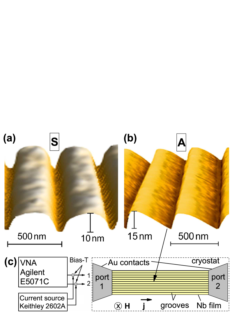
Combined broadband mw and dc electrical measurements were done in a 4He cryostat in the temperature range to with magnetic field directed perpendicular to the microstrip surface. A sketch of the experimental setup is shown in Fig. 1(c) and we refer to Ref. Dobrovolskiy, Franke, and Huth (2015) for a detailed description of the custom-made sample probe. In brief, the sample was mounted in a copper housing in which pins of the micro-SMP connectors were spring-loaded against the pre-formed nm-thick gold contact pads sputtered through a shadow mask onto the film surface after the nanopatterning step. The mw signal was fed to the sample through coaxial cables from an Agilent E5071C vector network analyzer (VNA). The mw and dc signals were superimposed and uncoupled by using two bias-tees mounted at the VNA ports. The VNA operated in the frequency sweep mode, with 1548 frequency () points scanned with an exponentially growing increment between KHz and GHz. The frequency traces of the cables and the connectors were excluded from the data so that the recorded dependences are due to the microstrips themselves and the vortex dynamics therein. The measured quantity is the forward transmission coefficient being the ratio (expressed in dB) of the mw power measured at port to the power transmitted at port . In what follows we use the notation for referring to its absolute value and primarily discuss the data for sample A. The data for the reference sample S are only commented when they are qualitatively different.
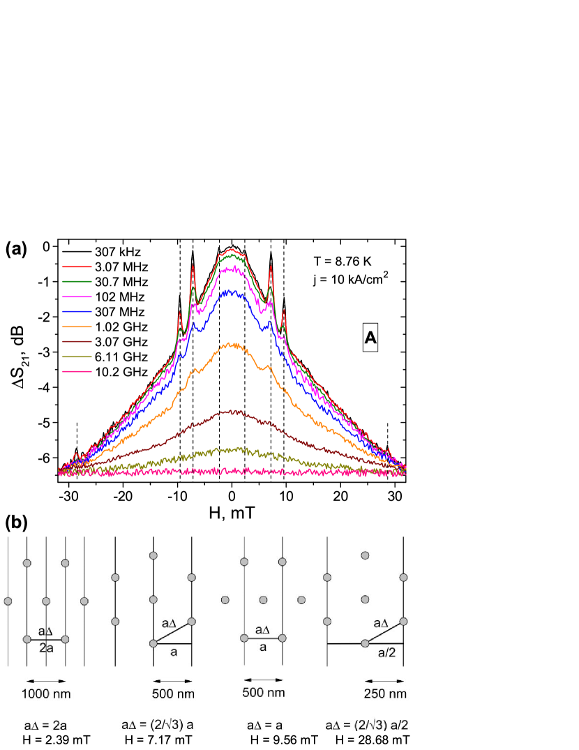
Figure 2(a) presents the relative change of the forward transmission coefficient for sample A as a function of the magnetic field at and a series of frequencies, as indicated. Here, stands for the mw loss in the transmission line (all cables, connectors etc.) and, hence, provides a measure for the mw loss due to vortex motion in the sample under study. For all frequencies, the mw excitation power at the sample is dBm (W) as kept by the VNA in accordance with the pre-saved calibration data for . The overall shape of the curves in Fig 2(a) is symmetric with respect to and we admit that the close-to-critical temperature of the measurement might have masked a field-polarity dependence peculiar to asymmetric potentials Plourde (2009). The data further attest to that at lower frequencies, the mw loss rises with increasing magnetic field, whereas becomes less sensitive to the field variation at elevated frequencies and saturates at the dB level (maximal loss). A detailed inspection of unveils a pronounced reduction of the mw loss (peaks in ) at mT and mT, while less pronounced peaks (recognizable at MHz) correspond to mT and mT. An increase of the microwave power by dB leads to the disappearance of these matching field effects as the sample is driven to the normal state. Here we would like to note that commensurability effects were recently observed in Pb films with square pinning site arrays by magnetic field-dependent mw power reflection spectroscopy Cuadra-Solis et al. (2014) and broadband permeability transmission measurements Lara et al. (2015). Also, the arrangement of vortices in a sawtooth, asymmetric pinning landscape was studied as a function of the vortex density by computer simulations Lu, Reichhardt, and Reichhardt (2007). While that system passed through a sequence of triangular, smectic, disordered and square vortex arrangements with increasing vortex density, the authors Lu, Reichhardt, and Reichhardt (2007) outlined the presence of triangular ordering in the vortex arrangement corresponding to one column of vortices per pinning trough and argued that this vortex lattice configuration is the most stable one. In the present case, for the assumed triangular vortex lattice with lattice parameter and the geometrical matching conditions , the arrangement of vortices with respect to the underlying pinning nanolandscape is shown in Fig. 2(b). The calculated field values for the triangular vortex lattices agree very well with those deduced from Fig. 2(a), although we cannot exclude the presence of more complex arrangements at fields 9.6 mT and 28.7 mT as suggested by simulations Lu, Reichhardt, and Reichhardt (2007). The field mT corresponds to the maximal vortex density when each vortex is pinned at the bottom of a groove and there are no interstitial vortices, i. e. to the fundamental matching configuration. It is this field for which the following findings are reported.
Figure 3(a) and (b) show the frequency dependence of sample A for the same magnitudes of positive and negative dc current densities at . In the absence of a dc bias, the mw loss is maximal at high frequencies, whereas the vortex response is weakly dissipative at low frequencies. For both dc bias polarities, upon increasing the dc value, the curves shift towards lower frequencies, see Fig. 3(a) and (b), but the magnitudes of the shifts substantially differ, whereas these nearly coincide for sample S (see supplementary figure See supplementary figure at http://… ). A series of curves for the positive polarity for sample S is shown in Fig. 3(f).
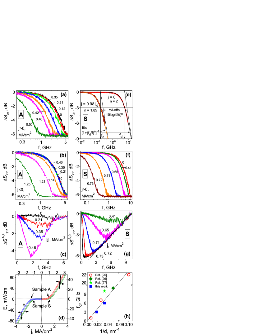
The reduction of the depinning frequency upon increasing the dc bias can be understood as a consequence of the effective lowering of the pinning potential well due to its tilt by the dc current. Indeed, the mechanistic consideration Shklovskij and Dobrovolskiy (2011) of a vortex as a particle leads to the conclusion that during an ac semiperiod, while the pinning potential well is broadening, with increasing the vortex has no longer time to reach the areas where the pinning forces dominate and, hence, the response becomes stronger dissipative already at lower frequencies, as compared with the zero-bias curve. The same mechanistic scenario can be applied for the explanation of the difference in the shifts of the depinning frequencies for the positive and the negative dc biases, caused by the different groove slope steepnesses Shklovskij, Sosedkin, and Dobrovolskiy (2014). Thus, by electrical resistance measurements we reveal that the groove asymmetry causes a difference in the depinning currents () for the positive and the negative branches of the CVC for sample A. At and mT these amount to MA/cm2 and MA/cm2, respectively. This is in contrast to the CVC of sample S which is symmetric with MA/cm2, see Fig. 3(d). Here, is determined by the V/cm electric field strength criterion. Therefore, sample A exhibits a microwave filter behavior, whose cut-off frequency depends not only on the dc value (as in sample S) but also on the dc polarity. In other words, provided one changes the dc polarity while keeping the dc current absolute value, the device is switched from one cut-off frequency to another.
To further corroborate our claim above, the difference signal for sample A is plotted in Fig. 3(c). One clearly sees the difference between the mw loss measured for the same, positive and negative dc bias magnitudes. This is caused by the fact that at moderate dc values (with respect to the corresponding ), for the gentle-slope direction of the vortex motion the depinning frequency is markedly lower than for the steep-slope direction. Specifically, the effect is most pronounced at MA/cm2 at which the depinning frequencies are GHz and GHz for the gentle-slope and the steep-slope direction, respectively. The depinning frequencies are determined at the dB loss level as shown in Fig. 3(e). In addition, we note that looks qualitatively similar to the difference signal for sample S in Fig. 3(g). There, the data at higher frequencies fall onto a universal, nearly straight line reminiscent of the respective frequency dependence observed in high- films patterned with an array of antidots Wördenweber et al. (2012).
To quantitatively describe the observed filter behavior, we fit the curves to the expression with the exponent for MA/cm2 and for for sample S. For the gentle-slope direction of sample A and for its steep-slope direction . In addition, in both cases drops by about at close-to-depinning biases. In general Pozar (2011), corresponds to a first-order filter roll-off related to the frequency characteristics of the microstrip as shown in Fig. 3(e). The reduced filter effectiveness at is attributed to smearing of the crossover due to heating effects and a more pronounced role played by inhomogeneities of the current distribution at close-to-depinning dc current densities. We also stress that the mw filter operates under the fundamental matching field condition and the reported here effects become entangled and eventually vanish upon tuning the field value away from 7.2 mT.
Finally, in Fig. 3(h) we plot the zero-bias depinning frequencies at and , , for both samples along with the data for Nb films reported by other authors Janjušević et al. (2006); Silva, Pompeo, and Sarti (2011); Pompeo et al. (2013). The values were estimated by the expression successfully used Zaitsev et al. (2003) for fitting the experimental data in high- films and the empiric dependence observed Janjušević et al. (2006) for Nb films, respectively. For our data, the field and temperature correction of to amounts to about , while it is notably larger for the data Janjušević et al. (2006); Silva, Pompeo, and Sarti (2011); Pompeo et al. (2013) acquired at higher temperatures and larger fields. For our samples, their thicknesses were taken after subtracting the groove depths, see Fig. 1. From Fig. 3(h) it follows that the cumulative data for Nb films can be fitted to the phenomenological law , where is the film thickness.
In summary, we have observed two major effects in nanopatterned Nb microstrips by combined dc and microwave measurements. These effects are (i) microwave loss reduction due to spatial commensurability of the vortex lattice with the underlying washboard nanopattern and (ii) a dual cut-off, dc-tunable microwave low-pass filter behavior of the sample with uniaxial asymmetric nanogrooves under the fundamental matching field condition. Since the effect of dc bias polarity-sensitive reduction of microwave losses may be exploited for tuning the properties of superconducting planar transmission lines, the reported results unveil an advanced microwave functionality of superconductors with an asymmetric (ratchet) pinning landscape. We furthermore anticipate that the observed filter behavior can be described by the results of Ref. Shklovskij, Sosedkin, and Dobrovolskiy (2014), while a detailed mapping of our findings on that model will be reported elsewhere.
OVD thanks Roland Sachser for automating the data acquisition and his help with the nanopatterning. Fruitful discussions with Valerij A. Shklovskij are gratefully acknowledged. This work was financially supported by the German Research Foundation (DFG) through grant DO 1511/2-4 and conducted within the framework of the NanoSC-COST Action MP1201 of the European Cooperation in Science and Technology.
References
- Wallraff et al. (2004) A. Wallraff, D. I. Schuster, A. Blais, L. Frunzio, R.-S. Huang, J. Majer, S. Kumar, S. M. Girvin, and R. J. Schoelkopf, Nature 431, 162 (2004).
- Hofheinz et al. (2009) M. Hofheinz, H. Wang, M. Ansmann, R. Bialczak, E. Lucero, M. Neeley, A. D. O’Connell, D. Sank, J. Wenner, J. M. Martinis, and A. N. Cleland, Nature 459, 546 (2009).
- DiCarlo et al. (2009) L. DiCarlo, J. M. Chow, J. M. Gambetta, L. S. Bishop, B. R. Johnson, D. I. Schuster, J. Majer, L. Blais, A. Frunzio, S. M. Girvin, and R. J. Schoelkopf, Nature 460, 240 (2009).
- Clarke and Wilhelm (2008) J. Clarke and F. K. Wilhelm, Nature 453, 1031 (2008).
- Song et al. (2009) C. Song, M. P. DeFeo, K. Yu, and B. L. T. Plourde, Appl. Phys. Lett. 95, 232501 (2009).
- Bothner et al. (2011) D. Bothner, T. Gaber, M. Kemmler, D. Koelle, and R. Kleiner, Appl. Phys. Lett. 98, 102504 (2011).
- Coumou et al. (2013) P. C. J. J. Coumou, E. F. C. Driessen, J. Bueno, C. Chapelier, and T. M. Klapwijk, Phys. Rev. B 88, 180505 (2013).
- Knufinke et al. (2012) M. Knufinke, K. Ilin, M. Siegel, D. Koelle, R. Kleiner, and E. Goldobin, Phys. Rev. E 85, 011122 (2012).
- Wördenweber et al. (2009) R. Wördenweber, E. Hollmann, J. Schubert, R. Kutzner, and A. K. Ghosh, Appl. Phys. Lett. 94, 202501 (2009).
- Zaitsev et al. (2007) A. G. Zaitsev, R. Schneider, R. Hott, T. Schwarz, and J. Geerk, Phys. Rev. B 75, 212505 (2007).
- Koelle et al. (1999) D. Koelle, R. Kleiner, F. Ludwig, E. Dantsker, and J. Clarke, Rev. Mod. Phys. 71, 631 (1999).
- Engel et al. (2012) A. Engel, A. Schilling, K. Il’in, and M. Siegel, Phys. Rev. B 86, 140506 (2012).
- Lahl and Wördenweber (2002) P. Lahl and R. Wördenweber, Appl. Phys. Lett. 81, 505 (2002).
- Awad et al. (2011) A. A. Awad, F. G. Aliev, G. W. Ataklti, A. Silhanek, V. V. Moshchalkov, Y. M. Galperin, and V. Vinokur, Phys. Rev. B 84, 224511 (2011).
- Cuadra-Solis et al. (2014) P.-d.-J. Cuadra-Solis, A. Garcia-Santiago, J. M. Hernandez, J. Tejada, J. Vanacken, and V. V. Moshchalkov, Phys. Rev. B 89, 054517 (2014).
- Jin et al. (2010) B. B. Jin, B. Y. Zhu, R. Wördenweber, C. C. de Souza Silva, P. H. Wu, and V. V. Moshchalkov, Phys. Rev. B 81, 174505 (2010).
- Wördenweber et al. (2012) R. Wördenweber, E. Hollmann, J. Schubert, R. Kutzner, and G. Panaitov, Phys. Rev. B 85, 064503 (2012).
- Gittleman and Rosenblum (1966) J. I. Gittleman and B. Rosenblum, Phys. Rev. Lett. 16, 734 (1966).
- Coffey and Clem (1991) M. W. Coffey and J. R. Clem, Phys. Rev. Lett. 67, 386 (1991).
- Brandt (1991) E. H. Brandt, Phys. Rev. Lett. 67, 2219 (1991).
- Shklovskij and Dobrovolskiy (2008) V. A. Shklovskij and O. V. Dobrovolskiy, Phys. Rev. B 78, 104526 (2008).
- Shklovskij and Dobrovolskiy (2011) V. A. Shklovskij and O. V. Dobrovolskiy, Phys. Rev. B 84, 054515 (2011).
- Shklovskij, Sosedkin, and Dobrovolskiy (2014) V. A. Shklovskij, V. V. Sosedkin, and O. V. Dobrovolskiy, J. Phys.: Cond. Matt. 26, 025703 (2014).
- Pompeo and Silva (2008) N. Pompeo and E. Silva, Phys. Rev. B 78, 094503 (2008).
- Janjušević et al. (2006) D. Janjušević, M. S. Grbić, M. Požek, A. Dulčić, D. Paar, B. Nebendahl, and T. Wagner, Phys. Rev. B 74, 104501 (2006).
- Silva, Pompeo, and Sarti (2011) A. Silva, N. Pompeo, and S. Sarti, Supercond. Sci. Technol. 24, 024018 (2011).
- Pompeo et al. (2013) N. Pompeo, K. Torokhtii, C. Meneghini, S. Mobilio, R. Loria, C. Cirillo, E. Ilyina, C. Attanasio, S. Sarti, and E. Silva, J. Supercond. Nov. Magnet. 26, 1939 (2013).
- Lara et al. (2015) A. Lara, F. G. Aliev, A. V. Silhanek, and V. V. Moshchalkov, Sci. Rep. 5, 9187 (2015).
- Dobrovolskiy and Huth (2012) O. V. Dobrovolskiy and M. Huth, Thin Solid Films 520, 5985 (2012).
- Dobrovolskiy et al. (2012) O. V. Dobrovolskiy, E. Begun, M. Huth, and V. A. Shklovskij, New J. Phys. 14, 113027 (2012).
- Pryadun et al. (2006) V. V. Pryadun, J. Sierra, F. G. Aliev, D. S. Golubovic, and V. V. Moshchalkov, Appl. Phys. Lett. 88, 062517 (2006).
- Aliev et al. (2009) F. G. Aliev, A. P. Levanyuk, R. Villar, J. F. Sierra, V. V. Pryadun, A. Awad, and V. V. Moshchalkov, New Journal of Physics 11, 063033 (2009).
- Cerbu et al. (2013) D. Cerbu, V. N. Gladilin, J. Cuppens, J. Fritzsche, J. Tempere, J. T. Devreese, V. V. Moshchalkov, A. V. Silhanek, and J. Van de Vondel, New J. Phys. 15, 063022 (2013).
- Silhanek, Van de Vondel, and Moshchalkov (2010) A. V. Silhanek, J. Van de Vondel, and V. V. Moshchalkov, “Guided vortex motion and vortex ratchets in nanostructured superconductors,” in Nanoscience and Engineering in Superconductivity (Springer-Verlag, Berlin Heidelberg, 2010) Chap. 1, pp. 1–24.
- (35) In the patterning process the beam parameters were kV/ pA, the dwell time was s, and the pitch was nm.
- Dobrovolskiy, Franke, and Huth (2015) O. V. Dobrovolskiy, J. Franke, and M. Huth, Meas. Sci. Technol. 26, 035502 (2015).
- Plourde (2009) B. L. T. Plourde, IEEE Trans. Appl. Supercond. 19, 3698 (2009).
- Lu, Reichhardt, and Reichhardt (2007) Q. Lu, C. J. O. Reichhardt, and C. Reichhardt, Phys. Rev. B 75, 054502 (2007).
- (39) See supplementary figure at http://… , .
- Pozar (2011) D. M. Pozar, Microwave engineering, 4th ed. (John Wiley & Sons, Inc., New York, 2011).
- Zaitsev et al. (2003) A. G. Zaitsev, R. Schneider, G. Linker, F. Ratzel, R. Smithey, and J. Geerk, Phys. Rev. B 68, 104502 (2003).