Observation of Anderson localization in ultrathin films of three-dimensional topological insulators
Abstract
Anderson localization, the absence of diffusive transport in disordered systems, has been manifested as hopping transport in numerous electronic systems, whereas in recently discovered topological insulators it has not been directly observed. Here we report experimental demonstration of a crossover from diffusive transport in the weak antilocalization regime to variable range hopping transport in the Anderson localization regime with ultrathin (Bi1-xSbx)2Te3 films. As disorder becomes stronger, negative magnetoconductivity due to the weak antilocalization is gradually suppressed, and eventually positive magnetoconductivity emerges when the electron system becomes strongly localized. This works reveals the critical role of disorder in the quantum transport properties of ultrathin topological insulator films, in which theories have predicted rich physics related to topological phase transitions.
pacs:
72.15.Rn, 73.20.Fz, 73.25.+iThe concept of Anderson localization has profoundly influenced our understanding of electron conductivity Abrahams10 . While examples for disorder driven metal-insulator transition are abundant in three-dimensions (3D), the question of whether Anderson transitions exist in 2D has posed a lot of theoretical and experimental challenges. Scaling theory proposed by Abrahams et al. predicts that there are no truly metallic states in non-interacting 2D electron systems Abrahams79 ; Lee85 . It was, however, discovered later that extended electron states may exist when electron-electron (e-e) interaction, spin-orbit coupling (SOC) or magnetic field comes in to play Evers08 ; Spivak10 . The 3D topological insulators (TIs) discovered in recent years Hasan10 ; Qi11 provide novel types of 2D electron systems that are of particular interest for study of the localization-delocalization problem. The Dirac surface states of 3D TIs are believed to be topologically protected from localization due to its special symmetry class Konig12 ; Fu12 ; Ostrovsky10 ; Ostrovsky07 ; Ryu07 . Moreover, when a 3D TI thin film is sufficiently thin, the hybridization between the top and the bottom surface states opens an energy gap near the Dirac point ZhangY10 , and it is suggested theoretically that the hybridization gap would drive the electron system to topologically different phase, such as a quantum spin Hall insulator or a trivial band insulator Linder09 ; LiuC10 ; Lu10 . Even though a lot of work has been carried out on electron transport properties of TI thin films Culcer12 ; Ando13 ; Bardarson13 ; YangWM13 , the fate of such electron systems under the condition of strong disorder (or in other words, whether Anderson localization could take place), still remains unclear.
In this work, we have studied electron transport in a large number of highly gate-tunable TI thin films with various thicknesses and chemical compositions. We found that only in ultrathin TI films in which surface hybridization and disorder effects are significant, hopping transport, a hallmark of strong localization Mott79 ; Shklovskii91 ; Ovadyahu99 , can be observed. The observed temperature and magnetic field dependences of conductivity suggest that electron transport can be driven from the diffusive transport governed by weak antilocalization (WAL) and e-e interactions to the Mott-type variable range hopping in the strong localization (i.e. Anderson localization) regime. The capability of tuning the surface states across a wide range of conductivity provides valuable insight into the nature of electron transport in the TI thin films.
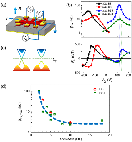
The electron transport measurements were carried out on Hall bar structures of (Bi1-xSbx)2Te3 and Bi2Se3 thin films (Fig. 1a). For the (Bi1-xSbx)2Te3 thin films with proper Bi:Sb ratio, ambipolar transport can be realized on a regular basis, owing to the low bulk carrier density in (Bi1-xSbx)2Te3 ZhangJ11 ; Kong11 as well as the large gate tunability offered by the SrTiO3 substrates Chen10 ; He12 . Effectively tuning the chemical potential in Bi2Se3 is more challenging due to the high excess electron densities (on the order of 1013 cm-2) brought by Se vacancies and other sources Analytis10 . Fig. 1b shows two examples of gate voltage tuning for (Bi1-xSbx)2Te3 thin films and two for Bi2Se3. For each sample, the maximum in the longitudinal resistance per square, , is located quite close to the gate voltage at which the Hall coefficient reverses its sign. This can be attributed to low sheet carrier densities of the bulk layer in the ultrathin TI films. The maximum can thus be regarded approximately as the charge neutral point (CNP) Kim12 . In the region near the CNP (usually located between the minimum and the maximum of ), both electrons and holes exist in the film. Outside this region, the transport is dominated by either holes (left, smaller ) or electrons (right, larger ), and the responses to gating are similar to those of p- or n-type semiconductors.
Fig. 1c schematically illustrates the change of surface states from gapless in thicker films to gapped in ultrathin films. According to a photoemission study of Bi2Se3 thin films, the hybridization between the top and bottom surfaces opens a noticeable energy gap when thickness is reduced to 5 quintuple layers (5 QL, 5 nm) or less, and the gap can be as large as 0.25 eV ZhangY10 . This can qualitatively explain the data shown in Fig. 1d, which summarizes the data from more than a dozen highly tunable (Bi1-xSbx)2Te3 and Bi2Se3 samples with various thicknesses. For the films thicker than 6 QL, is about 3 k, nearly independent of the thickness. In contrast, for QL increases rapidly with decreasing thickness. The small values obtained for thicker films are related to the gapless surface states, whereas the much larger observed in the thinner films can be attributed to the hybridization gap as well as stronger disorder effects.
By combining precise thickness control with the tuning of chemical composition and gate voltage, we were able to obtain values much larger than ( k) in the films with QL. The value can provide a convenient measure of how disordered the electron system is. The resistance is corresponding to in the Drude model, where is the dimensionless conductivity with , is the Fermi wavevector, and is the mean free path. Such a resistance defines the Ioffe-Regel criterion, which states that needs to be satisfied in a conductor Mott79 . The thickness dependence of shown in Fig. 1d suggests that the transport can be gradually tuned from the diffusive regime () Bergmann84 toward the strong localization regime (, corresponding to on the order of 100 k or higher) Mott79 ; Shklovskii91 .
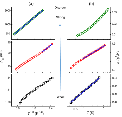
The change in the transport regime with increasing disorder is further manifested in the temperature dependence of conductivity depicted in Fig. 2. For large conductivity (1), logarithmic dependence on temperature was observed, consistent with previous measurements of TI thin films in the diffusive regime Chen11 ; LiuM11 ; Wang11 ; Takagaki12 ; Chiu13 ; Roy13 . For the TI surface states, the Berry phase associated with the spin-momentum locking leads to destructive interference for electron backscatterings and hence WAL, an effect opposite to the weak localization (WL) in ordinary 2D electron systems with negligible SOC. One would thus expect a type of increase in conductivity as drops. The e-e interactions Altshuler85 , however, produce a larger, opposite correction to the conductivity. The combined effects of WAL and e-e interactions can account for the observed -dependence in the weakly disordered regime Ostrovsky10 ; LuHZ14 . This is in contrast with , at which the transport was found to follow Mott’s law for the variable range hopping in 2D Mott79 ; Ovadyahu99 , namely . For intermediate conductivity (), there is a crossover from the logarithmic temperature dependence at higher to an exponential one at lower . This can be understood as a consequence of competition between dephasing length and localization length . An electron system can be regarded as strongly localized when and weakly (anti)localized when . At sufficiently low temperatures, the dephasing length is expected to follow since e-e interactions become the dominant source of dephasing Altshuler85 ; Lee12 ; Cha12 . Lowering temperature makes exceeding , and hence drives the crossover from WAL to strong localization. Similar transition can also be induced by varying the magnitude of disorder (see Fig. S6 in the online supplemental material Supplem ).
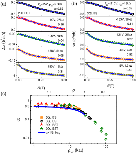
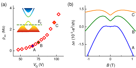
Such a change in the transport regime is also accompanied by a qualitative change in magnetoconductivity (MC), which is defined as . As shown in Fig. 3, the films with weak disorder exhibit negative MC, which is a consequence of suppression of WAL by the magnetic field Chen10 ; Checkelsky11 ; Chen11 ; Steinberg11 ; Kim12 . As disorder becomes stronger, the magnitude of the negative MC gradually decreases (Fig. 3a-b), and eventually when the transport is in the strong localization () regime, MC becomes positive in low magnetic fields (Fig. 4).
For weakly disordered TI thin films (), the negative MC due to WAL can often be satisfactorily described with a simplified Hikami-Larkin-Nagaoka (HLN) equation:
| (1) |
where is the digamma function, is the dephasing field, is the diffusion constant, and is the dephasing time. The prefactor is equal to 1/2 and for single channel transport in the WAL and the WL regimes, respectively. In TI thin films, however, multiple channels could be involved in the transport due to the existence of the top and bottom surface states, as well as possible conducting bulk. Nevertheless, has often been observed in TI thin films due to the coupling between various conducting channels Chen10 ; Chen11 ; Checkelsky11 ; Steinberg11 ; KimY11 ; Taskin12 ; Kim13 ; Lang13 ; Brahlek14 ; Garate12 .
In the strong localization regime, it is generally accepted that MC is positive regardless of the strength of SOC Shapir89 ; Wohlman89 ; Schirmacher90 ; Meir91 ; Shklovskii91 ; Hernandez92 ; ZhangYZ92 ; Hsu95 ; Lin98 . The positive MC observed in this regime can be attributed to the quantum interference between different paths for forward scatterings in the variable range hopping transport Shklovskii91 ; Lin98 ; Wohlman89 ; Schirmacher90 . It is different from the quantum corrections due to WAL (WL), in which the magnetic field suppresses the destructive (constructive) interference for backscattered paths Bergmann84 . Several groups suggested theoretically that the MC in the variable range hopping regime is quadratic in sufficiently weak magnetic fields and becomes linear (or nearly linear) at stronger fields Shklovskii91 ; Wohlman89 ; Schirmacher90 , until it reaches saturation at , where is the flux quantum and Rhop is the hopping distance ZhangYZ92 . As a result, the saturation field is expected to increase when the sample becomes more disordered. All of these features are qualitatively in agreement with the experimental data shown in Fig. 4b. As to the decrease in the MC observed at higher magnetic fields, it may be related to the field induced modifications of electron wavefunctions localized around impurities or defects, similar to that observed previously in semiconductors in the variable range hopping regime Shklovskii84 .
For an electron system with strong SOC, increasing the strength of disorder has been found previously to cause a change from the negative MC in the WAL regime to the positive MC in the strong localization regime. In an experiment with ultrathin metal films, Hsu and Valles observed that there is a well defined conductivity, (or , separating the samples with negative MC and those with positive MC Hsu95 . In the present work, however, we observed the change of sign of low field MC from negative to positive in the 2 QL thick (Bi1-xSbx)2Te3 film only when exceeds 0.5 M (or ), as shown in Fig. 4.
Also noteworthy is the intermediate regime between the diffusive and the hopping types of transport. This regime, with typically in the range of 10-100 k, can be readily achieved with 2-5 QL thick TI films. We found that the low field MC in the ultrathin films can be fitted fairly well with the HLN equation despite two orders of magnitude change in , as illustrated in Fig. 3a-b. Nevertheless, when is greater than 10 k, becomes to be smaller than the ordinary values (i.e. ) for WAL. The results from four highly tunable ultrathin films are summarized in Fig. 3c, which shows that there is a clear correlation between and : Beyond the diffusive regime, increasing leads to greater suppression of WAL (i.e. smaller ). When reaches 100 k, drops to nearly zero. It should be noted that remains positive as long as is smaller than 100 k.
Similar reductions in the values previously reported for TI ultrathin films Taskin12 ; Kim13 ; Lang13 ; KimY11 are also related to this intermediate disorder regime. An earlier study of 10 QL thick Ca-doped Bi2Se3 thin films also found substantial reduction of when is increased to 30 k Chen10 . It was pointed out by some of us Chen11 and subsequently by Brahlek et al. Brahlek14b that the transport beyond the diffusive regime needs to be considered to account for observed suppression of WAL. Knowledge learned from conventional semiconductors Minkov04 ; Lin98 and the data in Fig. 3 are useful to gain further insight. For disorder stronger than that required for well-defined diffusive transport, quantum corrections for higher order terms of need to be taken into account. In the case of weak SOC, Minkov et al. Minkov04 showed that the HLN equation could be valid, but the prefactor has to be reduced to . Correspondingly, one would expect as an extension to the case of WAL in ultrathin TI films. Fig. 3c shows that experimental values roughly follow this trend when . Further decreasing in conductivity (i.e. ) makes the perturbation treatment described in Ref. Minkov04 no longer valid. Nevertheless, values approaching zero obtained for are consistent with previous results on the traditional 2D electron systems with both weak Minkov04 and strong Lin98 SOC strengths. Such strong suppression of the negative MC can thus be interpreted as a result of the disorder-driven crossover from the so-called weakly insulating regime () toward the strong localization () regime. The positive MC and the variable range hopping transport related to the latter regime have not been observed perviously in TI materials.
Finally, we note that the suppression of WAL in ultrathin TI films may also take place as a consequence of a crossover from WAL to WL. Lu et al. LuHZ11 suggested that, when chemical potential is comparable to the hybridization gap , a spin texture with a spin component perpendicular to the surface develops, and the Berry phase is modified to =(1-/2). Therefore, tuning the chemical potential relative to the hybridization gap can in principle induce a crossover between WAL and WL. In this work, however, we were only able to observe the positive MC in the strong localization regime. We are also not aware of any previous work reporting observation of the positive MC with TI thin films in low magnetic fields while maintaining the electron transport in the weakly disordered (diffusive) regime. Therefore, significant improvement in the carrier mobility in ultrathin TI films is needed in order to unambiguously confirm the predicted crossover to WL due to the hybridization gap.
In summary, strong tuning of conductivity in the ultrathin TI films has allowed us to systematically study the transport properties from the WAL to the strong localization regime. Both temperature and disorder can drive such a crossover, which takes place when the phase coherence length exceeds the localization length. The suppression of negative MC and the appearance of positive MC in ultrathin TI films can be explained as a consequence of disorder-driven crossover between WAL and the strong localization. The topologically trivial insulating phases realized in ultrathin TI films Linder09 ; LiuC10 ; Lu10 may provide a valuable platform for pursuing topological Anderson insulators, a novel state of matter also driven by disorder LiJ09 ; JiangH09 ; Groth09 .
Acknowledgements.
Acknowledgements: We thank H. Jiang, H. Z. Lu, A. D. Mirlin, S. Q. Shen and J. R. Shi for stimulating discussions. This work was supported by the National Basic Research Program (Project No: 2012CB921703, 2012CB921300 & 2015CB921102), the National Science Foundation of China (Project Nos. 91121003, 11325421 & 61425015), and the Chinese Academy of Sciences.References
- (1) E. Abrahams (Editor), 50 Years of Anderson Localization (World Scientific, Singapore, 2010).
- (2) E. Abrahams, P. W. Anderson, D. C. Licciardello, and T. V. Ramakrishnan, Phys. Rev. Lett. 42, 673 (1979).
- (3) P. A. Lee and T. V. Ramakrishnan, Rev. Mod. Phys. 57, 287 (1985).
- (4) F. Evers and A.D. Mirlin, Rev. Mod. Phys. 80, 1355-1417 (2008).
- (5) B. Spivak, S. V. Kravchenko, S. A. Kivelson, and X. P. A. Gao, Rev. Mod. Phys. 82, 1743 (2010).
- (6) M. Z. Hasan and C. L. Kane, Rev. Mod. Phys. 82, 3045 (2010).
- (7) X. L. Qi and S. C. Zhang, Rev. Mod. Phys. 83, 1057 (2011).
- (8) E. J. Konig, P. M. Ostrovsky, I. V. Protopopov, and A. D. Mirlin, Phys. Rev. B. 85, 195130 (2012).
- (9) L. Fu and C. L. Kane, Phys. Rev. Lett. 109, 246605 (2012).
- (10) P. M. Ostrovsky, I. V. Gornyi, and A. D. Mirlin, Phys. Rev. Lett. 105, 036803 (2010).
- (11) P. M. Ostrovsky, I. V. Gornyi, and A. D. Mirlin, Phys. Rev. Lett. 98, 256801 (2007).
- (12) S. Ryu, C. Mudry, H. Obuse, and A. Furusaki, Phys. Rev. Lett. 99, 116601 (2007).
- (13) Y. Zhang, K. He, C. Z. Chang, C. L. Song, L. L. Wang, X. Chen, J. F. Jia, Z. Fang, X. Dai, W. Y. Shan, S. Q. Shen, Q. Niu, X. L. Qi, S. C. Zhang, X. C. Ma, and Q. K. Xue, Nat. Phys. 6, 584 (2010).
- (14) J. Linder, T. Yokoyama, and A. Sudbo, Phys. Rev. B 80, 205401 (2009).
- (15) C. X. Liu, H. J. Zhang, B. H. Yan, X. L. Qi, T. Frauenheim, X. Dai, Z. Fang, and S. C. Zhang, Phys. Rev. B 81, 041307(R) (2010).
- (16) H. Z. Lu, W. Y. Shan, W. Yao, Q. Niu, and S. Q. Shen, Phys. Rev. B 81, 115407 (2010).
- (17) D. Culcer, Physica E 44, 860 (2012).
- (18) Y. J. Ando, J. Phys. Soc. Jpn. 82, 102001 (2013).
- (19) J. H. Bardarson and J. E. Moore, Rep. Prog. Phys. 76, 056501 (2013).
- (20) W. M. Yang, C. J. Lin, J. Liao and Y. Q. Li, Chin. Phys. B 22, 097202 (2013).
- (21) N. F. Mott and G. A. Davis, Electronic Processes in Non-Crystalline Materials, 2nd ed. (Clarendon, Oxford, 1979).
- (22) B.I. Shklovskii and B.Z. Spivak, in Hopping Transport in Solids, M. Pollak and B. I. Shklovskii eds. (North-Holland, Amsterdam, 1991).
- (23) Z. Ovadyahu, Waves in Random Media 9, 241 (1999).
- (24) J. Zhang, C. Z. Chang, Z. C. Zhang, J. Wen, X. Feng, K. Li, M. H. Liu, K. He, L. L. Wang, X. Chen, Q. K. Xue, X. C. Ma, and Y. Y. Wang, Nat. Commun. 2, 574 (2011).
- (25) D. Kong, Y. L. Chen, J. J. Cha, Q. F. Zhang, J. G. Analytis, K. J. Lai, Z. K. Liu, S. S. Hong, K. J. Koski, S. K. Mo, Z. Hussain, I. R. Fisher, Z. X. Shen, and Y. Cui, Nat. Nanotech. 6, 705 (2011).
- (26) J. Chen, H. J. Qin, F. Yang, J. Liu, T. Guan, F. M. Qu, G. H. Zhang, J. R. Shi, X. C. Xie, C. L. Yang, K. H. Wu, Y. Q. Li, and L. Lu, Phys. Rev. Lett. 105, 176602 (2010).
- (27) X. Y. He, T. Guan, X. X. Wang, B. J. Feng, P. Cheng, L. Chen, Y. Q. Li, and K. H. Wu, Appl. Phys. Lett. 101, 123111 (2012).
- (28) J. G. Analytis, J. H. Chu, Y. L. Chen, F. Corredor, R. D. McDonald, Z. X. Shen, and I. R. Fisher, Phys. Rev. B 81, 205407 (2010).
- (29) D. Kim, S. Cho, N. P. Butch, P. Syers, K. Kirshenbaum, S. Adam, J. Paglione, and M. S. Fuhrer, Nat. Phys. 8, 459 (2012).
- (30) G. Bergmann, Phys. Rep. 107, 1 (1984).
- (31) J. Chen, X. Y. He, K. H. Wu, Z. Q. Ji, L. Lu, J. R. Shi, J. H. Smet, and Y. Q. Li, Phys. Rev. B 83, 241304 (R) (2011).
- (32) M. H. Liu, C. Z. Chang, Z. C. Zhang, Y. Zhang, W. Ruan, K. He, L. L. Wang, X. Chen, J. F. Jia, S. C. Zhang, Q. K. Xue, X. C. Ma, and Y. Y. Wang, Phys. Rev. B 83, 165440 (2011).
- (33) J. Wang, A. M. DaSilva, C. Z. Chang, K. He, J. K. Jain, N. Samarth, X. C. Ma, Q. K. Xue, and M. H. W. Chan, Phys. Rev. B 83, 245438 (2011).
- (34) Y. Takagaki, B. Jenichen, U. Jahn, M. Ramsteiner, and K. J. Friedland, Phys. Rev. B 85, 115314 (2012).
- (35) S. P. Chiu and J. J. Lin, Phys. Rev. B 87, 035122 (2013).
- (36) A. Roy, S. Guchhait, S. Sonde, R. Dey, T. Pramanik, A. Rai, H. C. P. Movva, L. Colombo, and S. K. Banerjee, Appl. Phys. Lett. 102, 163118 (2013).
- (37) B. L. Altshuler and A. G. Aronov, in Electron-Electron Interactions in Disordered Conductors, A. L. Efros and M. Pollak eds. (North-Holland Physics Publishing, 1985).
- (38) H. Z. Lu and S. Q. Shen, Phys. Rev. Lett. 112, 146601 (2014).
- (39) J. Lee, J. Park, J. H. Lee, J. S. Kim, and H.-J. Lee, Phys. Rev. B 86, 245321 (2012).
- (40) J. J. Cha, D. S. Kong, S.-S. Hong, J. G. Analytis, K. J. Lai, and Y. Cui, Nano Lett. 12, 1107 (2012).
- (41) Supplemental Material, which includes Refs. JiangYP12 ; Minkov07 , is available upon request.
- (42) Y. P. Jiang, Y. L. Wang, M. Chen, Z. Li, C. L. Song, K. He, L. L. Wang, X. Chen, X. C. Ma, and Q.-K. Xue, Phys. Rev. Lett. 108, 016401 (2012).
- (43) G. M. Minkov, A. V. Germanenko, O. E. Rut, A. A. Sherstobitov, and B. N. Zvonkov, Phys. Rev. B 75, 235316 (2007).
- (44) J. G. Checkelsky, Y. S. Hor, R. J. Cava and N. P. Ong, Phys. Rev. Lett. 106, 196801 (2011).
- (45) H. Steinberg, J. B. Laloe, V. Fatemi, J. S. Moodera, and P. Jarillo-Herrero, Phys. Rev. B 84, 233101 (2011).
- (46) A. A. Taskin, S. Sasaki, K. Segawa, and Y. Ando, Phys. Rev. Lett. 109, 066803 (2012).
- (47) D. Kim, P. Syers, N. P. Butch, J. Paglione, and M. S. Fuhrer, Nat. Commun. 4, 2040 (2013).
- (48) M. Lang, L. He, X. Kou, P. Upadhyaya, Y. Fan, H. Chu, Y. Jiang, J. H. Bardarson, W. Jiang, E. S. Choi, Y. Wang, N. C. Yeh, J. Moore, and K. L. Wang, Nano Lett. 13, 48 (2013).
- (49) M. Brahlek, N. Koirala, M. Salehi, N. Bansal, and S. Oh, Phys. Rev. Lett. 113, 026801 (2014).
- (50) Y. S. Kim, M. Brahlek, N. Bansal, E. Edrey, G. A. Kapilevich, K. Iida, M. Tanimura, Y. Horibe, S. W. Cheong, and S. Oh, Phys. Rev. B 84, 073109 (2011).
- (51) I. Garate and L. Glazman, Phys. Rev. B 86, 035422 (2012).
- (52) Y. Shapir and Z. Ovadyahu, Phys. Rev. B 40, 12441 (1989).
- (53) O. Entin-Wohlman, Y. Imry and U. Sivan, Phys. Rev. B 40, 8342 (1989).
- (54) W. Schirmacher, Phys. Rev. B 41, 2461 (1990).
- (55) Y. Meir, N. S. Wingreen, O. Entin-Wohlman and B. L. Altshuler, Phys. Rev. Lett. 66, 1517 (1991).
- (56) P. Hernandez and M. Sanquer, Phys. Rev. Lett. 68, 1402 (1992).
- (57) Y. Z. Zhang, P. H. Dai and M. P. Sarachik, Phys. Rev. B 45, 9473-9476 (1992).
- (58) S. Y. Hsu and J. M. Valles, Phys. Rev. Lett. 74, 2331 (1995).
- (59) Y. L. Lin, Phys. Rev. B 58, 13544 (1998).
- (60) B. I. Shklovskii and A. L. Efros, Electronic Properties of Doped Semiconductors (Springer-Verlag, Berlin, 1984).
- (61) G. M. Minkov, A. V. Germanenko and I. V. Gornyi, Phys. Rev. B 70, 245423 (2004).
- (62) M. Brahlek, N. Koirala, N. Bansal, and S. Oh, e-print arXiv:1408.1614.
- (63) H. Z. Lu, J. R. Shi and S. Q. Shen, Phys. Rev. Lett. 107 076801 (2011).
- (64) J. Li, R. L. Chu, J. K. Jain, and S. Q. Shen, Phys. Rev. Lett. 102, 136806 (2009).
- (65) H. Jiang, L. Wang, Q.-F. Sun, and X. C. Xie, Phys. Rev. B 80, 165316 (2009).
- (66) C. W. Groth, M. Wimmer, A. R. Akhmerov, J. Tworzydlo, and C. W. J. Beenakker, Phys. Rev. Lett. 103, 196805 (2009).