Spin splitting in 2D monochalcogenide semiconductors
Abstract
We report ab initio calculations of the spin splitting of the uppermost valence band (UVB) and the lowermost conduction band (LCB) in bulk and atomically thin GaS, GaSe, GaTe, and InSe. These layered monochalcogenides appear in four major polytypes depending on the stacking order, except for the monoclinic GaTe. Bulk and few-layer - and -type, and odd-number -type GaS, GaSe, and InSe crystals are noncentrosymmetric. The spin splittings of the UVB and the LCB near the -point in the Brillouin zone are finite, but still smaller than those in a zinc-blende semiconductor such as GaAs. On the other hand, the spin splitting is zero in centrosymmetric bulk and even-number few-layer -type GaS, GaSe, and InSe, owing to the constraint of spatial inversion symmetry. By contrast, GaTe exhibits zero spin splitting because it is centrosymmetric down to a single layer. In these monochalcogenide semiconductors, the separation of the non-degenerate conduction and valence bands from adjacent bands results in the suppression of Elliot-Yafet spin relaxation mechanism. Therefore, the electron- and hole-spin relaxation times in these systems with zero or minimal spin splittings are expected to exceed those in GaAs when the D’yakonov-Perel’ spin relaxation mechanism is also suppressed.
I Introduction
Potential applications in spin-dependent electronics and optoelectronics have driven the search for materials capable of exhibiting a high degree of spin polarization and long spin relaxation time Žutić et al. (2004); Dyakonov (2008). However, optical generation of electron and hole spin polarization and resulting polarized luminescence are typically limited by the mixing of degenerate valence bands in most semiconductors Dyakonov (2008). Recent reports of valley polarization in atomically thin transition metal dichalcogenides (TMDs) Xiao et al. (2012); Cao et al. (2012); Zeng et al. (2012); Mak et al. (2012); Xu et al. (2014) suggest potential exploitation of both spin and valley degrees of freedom for electronics and optoelectronics. In an experimental study Tang et al. (2015), we demonstrated the high generation and preservation of optical spin polarization and dynamics in a group-III monochalcogenide, GaSe, under nonresonant optical pumping. The observed near unity optical spin polarization Gamarts et al. (1977); Ivchenko et al. (1977) is attributed to suppressed electron and hole spin relaxation rates resulting from reduced valence-band mixing. However, the microscopic spin relaxation mechanisms in GaSe and related monochalcogenides are not fully understood.
In metals and semiconductors, the major spin relaxation mechanisms– including Elliott-Yafet (EY) Elliott (1954); Yafet (1963) and D’yakonov-Perel’ (DP) D’yakonov and Perel’ (1971, 1972, 1984) mechanisms– are associated with the spin-orbit interaction (SOI) and the spin-orbit-induced spin splitting, Dyakonov (2008); Boross et al. (2013). Considering spin-relaxation with a four-state (two bands with spin) model Hamiltonian in the absence of an external magnetic field, one can relate the spin relaxation rate of electrons (holes) when the Fermi energy (corresponding to Fermi vector ) is away from the conduction (valence) band edge with the following equation Boross et al. (2013):
| (1) |
where is the scattering rate of the electron/hole, with being the corresponding momentum scattering (or correlation) time, being the spin-orbit-induced spin splitting, and being the SOI between the adjacent bands with energy separation . In GaSe, the -like uppermost valence band (UVB) is well isolated from the lowermost conduction band (LCB) (2 eV) and the adjacent -like valence bands, and as a result 0.02–0.04 Kuroda et al. (1980); Kuroda and Nishina (1981). The hole-spin relaxation due to the EY mechanism is thus expected to be much smaller than the momentum relaxation rate . The spin relaxation caused by the DP mechanism can be seen as being due to the precession of spins in an effective magnetic field associated with D’yakonov and Perel’ (1984); Dyakonov (2008); Boross et al. (2013). The DP spin relaxation rate is proportional to the spin splitting, , where is the momentum relaxation time. Therefore, when the spin relaxation is dominated by the DP mechanism, the smaller the spin splitting, the longer the spin relaxation time for the same momentum relaxation rate .
To understand the spin relaxation, one first needs the momentum()-dependent of the bands near the fundamental gap. In the absence of magnetic fields, is zero in centrosymmetric crystals because of the constraints of time-reversal symmetry [, Kramers degeneracy] and spatial inversion symmetry []. When the inversion symmetry is broken in crystals (bulk inversion asymmetry (BIA)) Dresselhaus (1955) or heterostructures (structural inversion asymmetry (SIA)) Bychkov and Rashba (1984); Winkler (2000), is finite, and only the Kramers degeneracy is left. Understanding in GaAs and other zinc-blende semiconductors has been a subject of considerable interest Yu et al. (2005); Chantis et al. (2006, 2010); Luo et al. (2009, 2010); Shen and Wu (2010) since the seminal work of Dresselhaus Dresselhaus (1955). Ab initio calculations, such as LDA (or GGA) and self-consistent GW methods, of in bulk GaAs and two-dimensional GaAs-based superlattices and heterostructures have improved the understanding of the spin splitting Chantis et al. (2006, 2010); Luo et al. (2009, 2010). A few theoretical calculations of in TMDs also have been reported Zhu et al. (2011); Chang et al. (2014). In this study, we report ab initio calculations of of the uppermost valence band (UVB) and the lowermost conduction band (LCB) in GaSe and related group-III monochalcogenides, including GaS, GaTe, and InSe.
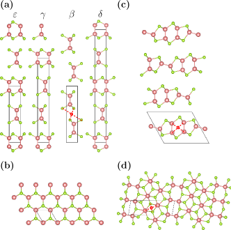
Monochalcogenides ( = \ceGa, \ceIn; = S, Se) crystallize in hexagonal layered structures Madelung (2004) (Fig. 1) of four major polytypes, namely , , , and (Fig. 1a), depending on the stacking order (hereinafter referred to as crystals). -, -, -, and - crystals belong to the space group (Schoenflies notation) of , , , and , respectively. Monolayer crystals (space group ) are noncentrosymmetric. Bulk -, -, and - crystals, which appear in an AB, ABC, and ABCD stacking order, are noncentrosymmetric, while - crystals are centrosymmetric with an AB stacking order. Additionally, there are two exceptions: (1) an atomically thin - crystal with even-number layers is centrosymmetric, and (2) a bilayer - crystal can be identical to either a bilayer - crystal (noncentrosymmetric) or a bilayer - crystal (centrosymmetric) depending on which two layers are isolated from a bulk - crystal. GaTe appears as a distorted form of the structure, where one out of three Ga-Ga bonds lies in the - plane (Fig. 1c–d). In contrast to crystals, GaTe crystals belong to the monoclinic lattice system (space group ), and are centrosymmetric down to a single layer Madelung (2004).
Bulk and few-layer - and -type, as well as odd-number few-layer -type GaS, GaSe, and InSe crystals finite spin splittings, while bulk and even-number few-layer -type GaS, GaSe, and InSe as well as GaTe crystals exhibit zero spin splitting. The difference is due to the constraints of the aforementioned time-reversal and spatial inversion symmetry (or the lack of it).
II Computational Methods
We compute the band structures and of valence and conduction bands with the projector augmented wave method as implemented in the VASP Kresse and Hafner (1993); Kresse and Furthmüller (1996, 1996); Kresse and Joubert (1999); Blöchl (1994) package and the full-potential (linearized) augmented plane-wave as implemented in the WIEN2k Schwarz and Blaha (2003); Singh and Nordström (2006) package. The band structures are calculated with the WIEN2k package, with the optimized crystal structures determined by minimizing the total energy with all electrons (including core electrons) with VASP. In all calculations, exchange-correlation energies are determined by the Perdew-Burke-Ernzerhof (PBE) Perdew et al. (1996) generalized gradient approximation (GGA) Martin (2004), which systematically underestimates the band gaps and produces dispersions (effective masses) different from experimental values. These shortcomings of the GGA also limit the accuracy of the calculated .
The spin-orbit interaction (SOI) is included in our calculations of the overall band structure and the spin splitting of a given band in a self-consistent manner using a second variation approach Koelling and Harmon (1977); MacDonald et al. (1980); Kleinman (1980). The SOI Hamiltonian in the spherical symmetric potential can be represented as: , where is the electron mass, c the speed of light, and the orbital and spin momentum vectors, and an effective single particle local potential seen by the electron. This form of is correct as long as is local and isotropic. In Hartree approximation and LDA, the effective potential is indeed local, though it is not always isotropic. The isotropic approximation is valid because the dominant contribution to is from regions near the nucleus. However, local approximations do not give correct band structure near the band gap. The accuracy of the band gap can be improved with hybrid models such as the Heyd-Scuseria-Ernzerhof (HSE06) Heyd et al. (2003) (a mixture of non-local and local exchange) or GW-like theories. In these approximations, the aforementioned simple form of is not necessarily valid Blume and Watson (1962, 1963). A compromised approach invloves calculating the band structure using non-local or GW theories while calculating the spin splitting with a local form of the and the LDA potential Chantis et al. (2006); Sakuma et al. (2011). Nonetheless, one has to examine uncertainties in these hybrid calculations critically.
To model a few-layer thin film, we create a supercell (supercell method Martin (2004)) containing one few-layer structure and a 15–25 Å thick vacuum spacer, which is large enough to suppress interactions arising from the artificial periodicity present in the supercell method. The crystalline -axis of the supercell is set perpendicular to the crystalline - plane. In this way, one can distinguish the effects of intra- and inter-layer interactions on the electronic structures in few-layer structures. The number of atoms in a unit cell is as follows: eight for - and -, twelve for -, sixteen for -, and twelve for monoclinic GaTe. To obtain an energy accuracy of 0.1 meV in self-consistent calculations, we use -centered Monkhorst–Pack Monkhorst and Pack (1976) -meshes of and for bulk and few-layer GaSe-type structures, respectively. For GaTe, we use meshes of and for bulk and few-layer GaTe, respectively.
III Results
III.1 Band structure: bulk versus single-layer
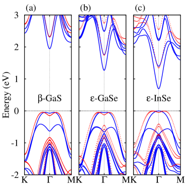
In Fig. 2, we show the electronic band structures of bulk and monolayer -GaS, -GaSe, and -InSe, which are the most naturally abundant. The general features of the electronic band structures, except the spin splitting, are nearly polytype-independent, owing to the weak inter-layer interactions. The lowermost conduction band (LCB) has -like symmetry, whereas the two uppermost valence bands (UVBs) have -like symmetry. The -like valence bands appear 1 eV below the UVB as a result of the crystal field and SOI. The calculated band structures for -GaSe show a nearly direct band gap at the -point of the Brillouin zone (BZ), where a valley appears in the UVB. The energy of the LCB at the -point is 0.5 eV lower than that at the M point, consistent with the hybrid density functional calculations Zólyomi et al. (2013). On the contrary, tight binding calculations show that the energy of the LCB at the M point for GaSe is 10 meV below that at the -point in the BZ Camara et al. (2002).
The band gap is seen to decrease with increasing atomic number (GaIn or SSe). The calculated band gaps are 2.0 eV, 1.3 eV, and 0.71 eV for -GaS, -GaSe, and -InSe, respectively, which are each smaller than the experimental values (3.1 eV, 2.0 eV, and 1.3 eV) Madelung (2004). The band-gap underestimation can be remedied with, for example, the HSE06 hybrid functional Heyd et al. (2003); Zólyomi et al. (2013); Zhuang and Hennig (2013). In the absence of SOI, the states are doubly degenerate at the -point. On the other hand, the SOI lifts this energy degeneracy with a spin-orbit splitting 0.09 eV, 0.34 eV, and 0.31 eV in GaS, GaSe, and InSe, respectively. in GaSe and InSe are similar in magnitude, but a factor of three smaller in GaS, agreeing with previously reported calculations Mooser and Schlüter (1973); Schlüter et al. (1976); Doni et al. (1979); Depeursinge (1981). in GaS is minimal, as expected from the weak SOI in the lighter S anions which govern the characteristics of the few uppermost valence bands of GaS. Monolayer GaS, GaSe, and InSe have very similar band structures (Fig. 2). We note two different features in the band structures of monolayer s in comparison with their bulk counterparts: (1) the quantum confinement along the -axis increases the band gap to 2.36 eV, 1.78 eV, and 1.4 eV for GaS, GaSe and InSe, respectively, and (2) the band gap becomes indirect as the valley at the -point becomes wider in momentum () and deeper in energy ().
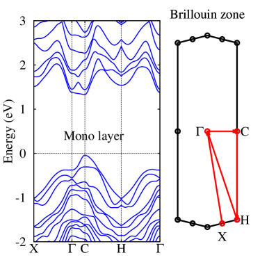
The band structure of GaTe (bulk) has also been calculated with GGA Sánchez-Royo et al. (2002); Rak et al. (2009), showing a direct band gap of 1 eV. The inclusion of SOI causes negligible changes in the UVB and LCB of GaTe. Monolayer GaTe shows a direct band gap of 1.4 eV (Fig. 3), with LCB having two nearly degenerate minima at the and C points. At the C point, LCB has -like symmetry while the UVB has -like symmetry. SOI removes the degeneracy of valence bands at , with eV. is smaller in GaTe than in GaSe despite Te being heavier than Se. The reduction in the strength of is due to the quenching of orbital angular momentum in the lower symmetry crystalline structure, as demonstrated by a sizable 0.7 eV calculated for a hypothetical -type GaTe (space group ).
III.2 Spin splitting
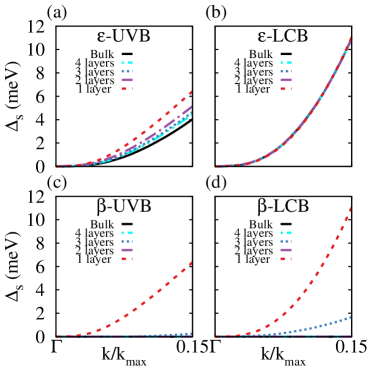
In Fig. 4, we show the spin splittings of the UVB () and the LCB () along the –K direction in - and -GaSe. The spin splitting along the –M direction is zero, obeying the constraint of spatial inversion symmetry. Both and decrease with the number of layers, approaching those in the bulk. At ( is at the K point in the BZ), 6 meV and 4 meV for monolayer and bulk -GaSe, respectively. The nearly layer-independent LCB spin splitting has a value meV at , which is slightly larger than .
In contrast to -GaSe, bulk and even-number few-layer -\ceGaSe crystals have zero spin splitting (Fig. 4c–d), obeying the constraint of spatial inversion symmetry. The and in odd-number few-layer -GaSe crystals are finite, but diminish rapidly with increasing layers. In trilayer -GaSe, the UVB spin splitting is less than 1 meV, and LCB spin splitting is smaller by a factor of five compared to that of the monolayer. The thickness dependent spin splitting in -GaSe presented here are consistent with those reported in \ceMoS2 Chang et al. (2014), which has the same symmetry as -GaSe. Bulk -GaSe has similar spin splittings as bulk -GaSe, with decreasing spin splittings as the number of layers increase.
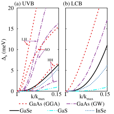
In Fig. 5, we compare and in monolayer GaS, GaSe, and InSe (group-III monochalcogenides) and bulk GaAs (a representative zinc-blende III-V semiconductor). Among the monolayer group-III monochalcogenides, overall spin splittings decrease from GaSe, to InSe, and then to GaS. The spin splittings typically increase with the increasing atomic number of constituent atoms as result of the enhanced SOI in the heavier atoms. However, other details of the band structure such as the band gap also contribute to the spin splittings.
The valence band of GaAs consists of a heavy hole (HH), a light hole (LH), and a split-off (SO) band Yu et al. (2005); Shen and Wu (2010). The calculated HH spin splitting is close to that in the UVB of GaSe. However, the spin splittings in the LH and SO bands are at least a factor of two larger than that in the UVB of GaSe. The calculated overall LCB spin splitting in GaAs is also larger than that in GaSe. The magnitude at = 0.15 is more than two times larger in GaAs than in GaSe. The spin splitting of the heavy-hole band is reduced by about a factor of two when the GW method is used in lieu of the GGA method.
IV Discussion
| Band | UVB | LCB | ||
|---|---|---|---|---|
| Coefficient | (meV) | (eV) | (meV) | (eV) |
| Monolayer | 1.0 | 4.9 | 0.3 | 4.7 |
| 2-layer | 2.9 | 2.6 | 2.0 | 4.2 |
| 3-layer | 0.3 | 3.0 | 0.4 | 4.8 |
| 4-layer | 0.6 | 2.6 | 0.4 | 4.9 |
| 5-layer | 0.3 | 2.5 | 0.4 | 4.9 |
| 6-layer | 0.4 | 2.4 | 0.4 | 4.9 |
| Bulk | 0.1 | 2.2 | 0.2 | 5.0 |
The spin splittings discussed above concern mainly the overall spin splitting up to = 0.15. To understand the spin relaxation mechanisms, we need to identify the -dependence of the spin splitting in the vicinity of the -point. At small , the theory predicts that, in noncentrosymmetric zinc-blende and wurtzite structures, the -dependence of the spin splitting contains both a linear and a cubic term when the core levels are considered Dresselhaus (1955); Cardona et al. (1986); Luo et al. (2010); Lew Yan Voon et al. (1996). To illustrate the -dependence of the spin splitting, we fit the calculated in -GaSe with the function for 0.05 (Table 1). The energy scales for the coefficients (meV) and (eV) are consistent with those determined from GW calculations for GaAs Chantis et al. (2006); Luo et al. (2010). Although is three to four orders of magnitude larger than , there exists a crossover value of below which the linear term dominates. In contrast to the GaAs case where the linear term is negligible for the LCB, we find a sizable linear term for the LCB in GaSe. The cubic coefficient for the LCB is 4–5 eV for the monolayer to the bulk, with the bilayer case being slightly different. In contrast to the UVB, there appears to be an odd-even-layer effect: values for the odd layers (1 and 3) are larger, but are close to the bulk values for the even layers (2 and 4). For the LCB, the values are similar for all the layers, except for the bilayer ( = 2.0 meV) and the bulk ( = 0.2 meV). Note that bilayer GaSe has an unusually large value, and for the UVB, there appears to be an odd-even effect like that in the LCB. The value for the bilayer is nearly three times that for the monolayer, whereas for the four-layer is two times that for the trilayer. As pointed out in the case of GaAs, these subtle differences are due to the characteristics of the UVB and LCB energy values and wave functions, and their mixing with other bands including the core levels Dresselhaus (1955); Cardona et al. (1986); Luo et al. (2010).
The DFT-based theories such as LDA (or GGA) underestimate band gaps and do not give accurate effective masses, resulting in overestimated Chantis et al. (2006); Luo et al. (2009, 2010). GW calculations reproduce more accurate band parameters, such as the band gap and effective mass, but are computationally more intensive than LDA (GGA) calculations. For simplicity, in this work, we have used GGA to calculate . The GGA calculation underestimates the GaAs band gap by a factor of ten; however, the spin splitting only deviates from that determined by the GW calculation by a factor of two. The band gaps are underestimated by the GGA for GaSe and related monochalcogenides by a factor of approximately two, which is significantly less than that for GaAs. For example, in GaSe, the GGA calculation gives a band gap of about 1 eV, which is off from the GW/HSE06 calculation Zhuang and Hennig (2013) and the measured band gap (2 eV) Mooser and Schlüter (1973) by a factor of two. Therefore, we expect the GGA calculation to produce spin splittings close to the value obtained with the GW calculation. We also expect similar variations of with from one conduction/valence band to another and from bulk to atomically thin layers.
V Conclusion
We present a systematic study of spin-orbit-induced spin splittings bulk and atomically thin group-III monochalcogenides ( = Ga, In; = S, Se, Te). The spin splitting vary with anion element and crystal symmetry. Centrosymmetric crystals, including bulk -type GaS, GaSe, and InSe, as well as monoclinic GaTe down to the monolayer, have zero spin splitting, as anticipated from the constraints of spatial inversion symmetry and time-reversal symmetry. In these monochalcogenide semiconductors, the separation of the non-degenerate conduction and valence bands from other adjacent bands results in suppression of Elliot-Yafet spin relaxation mechanism. Therefore, the electron and hole spin relaxation times in these systems with zero or minimal spin splittings and reduced valence-band mixing are expected to be longer than those in a zinc-blende semiconductor (eg., GaAs Hilton and Tang (2002); Yu et al. (2005); Shen and Wu (2010)), owing to the suppression of D’yakonov-Perel’ and Elliot-Yafet spin relaxation mechanisms.
Acknowledgements.
This work was supported by NSF grant DMR-09055944 as well as a start-up funding and the J. Cowen endowment at Michigan State University. The calculations were performed with computational resource provided by Institution for Cyber Enabled Research (ICER) and High Performance Computer Center (HPCC) at Michigan State University.References
- Žutić et al. (2004) I. Žutić, J. Fabian, and S. Das Sarma, “Spintronics: Fundamentals and applications,” Rev. Mod. Phys. 76, 323–410 (2004).
- Dyakonov (2008) M. I. Dyakonov, ed., Spin Physics in Semiconductors, Springer Series in Solid-State Science, Vol. 157 (Springer, 2008).
- Xiao et al. (2012) D. Xiao, G-B . B. Liu, W. Feng, X. Xu, and W. Yao, “Coupled spin and valley physics in monolayers of MoS2 and other group-VI dichalcogenides,” Phys. Rev. Lett. 108, 196802 (2012).
- Cao et al. (2012) T. Cao, G. Wang, W. Han, H. Ye, C. Zhu, J. Shi, Q. Niu, P. Tan, E. Wang, B. Liu, and J. Feng, “Valley-selective circular dichroism of monolayer molybdenum disulphide,” Nature Commun. 3, 887 (2012).
- Zeng et al. (2012) H. Zeng, J. Dai, W. Yao, D. Xiao, and X. Cui, “Valley polarization in MoS2 monolayers by optical pumping,” Nature Nanotech. 7, 490 (2012).
- Mak et al. (2012) K. F. Mak, K. He, J. Shan, and T. F. Heinz, “Control of valley polarization in monolayer MoS2 by optical helicity,” Nature Nanotech. 7, 494 (2012).
- Xu et al. (2014) X. Xu, W. Yao, D. Xiao, and T. F. Heinz, “Spin and pseudospins in layered transition metal dichalcogenides,” Nature Phys. 10, 343 (2014).
- Tang et al. (2015) Y. Tang, W. Xie, K. C. Mandal, J. A. McGuire, and C. W. Lai, “Optical and spin polarization dynamics in GaSe nanoslabs,” Phys. Rev. B 91, 195429 (2015).
- Gamarts et al. (1977) E. M. Gamarts, E. L. Ivchenko, M. I. Karaman, V. P. Mushinskii, G. E. Pikus, B. S. Razbirin, and A. N. Starukhin, “Optical orientation and alignment of free excitons in GaSe during resonance excitation. experiment,” Sov. Phys. JETP 46, 590 (1977).
- Ivchenko et al. (1977) E. L. Ivchenko, G. E. Pikus, B. S. Razbirin, and A. I. Starukhin, “Optical orientation and alignment of free excitons in GaSe under resonant excitation. theory.” Sov. Phys. JETP 45, 1172–1180 (1977).
- Elliott (1954) R. J. Elliott, “Theory of the effect of spin-orbit coupling on magnetic resonance in some semiconductors,” Phys. Rev. 96, 266–279 (1954).
- Yafet (1963) Y. Yafet, “g factors and spin-lattice relaxation of conduction electrons,” in Solid State Physics, Solid State Physics, Vol. 14 (Academic Press, 1963) pp. 1–98.
- D’yakonov and Perel’ (1971) M. I. D’yakonov and V. I. Perel’, “Spin orientation of electrons associated with the interband absorption of light in semiconductors,” Sov. Phys. JETP 33, 1053 (1971).
- D’yakonov and Perel’ (1972) M. I. D’yakonov and V. I. Perel’, “Spin relaxation of conduction electrons in noncentrosymmetric semiconductors,” Sov. Phys. Solid State 13, 3023–3026 (1972).
- D’yakonov and Perel’ (1984) M. I. D’yakonov and V. I. Perel’, “Theory of optical spin orientation of electrons and nuclei in semiconductors,” in Optical Orientation, Modern Problems in Condensed Matter Sciences, Vol. 8 (Elsevier, 1984) pp. 11–72.
- Boross et al. (2013) P. Boross, B. Dóra, A. Kiss, and F. Simon, “A unified theory of spin-relaxation due to spin-orbit coupling in metals and semiconductors,” Sci. Rep. 3, 3233 (2013).
- Kuroda et al. (1980) N. Kuroda, I. Munakata, and Y. Nishina, “Exciton transitions from spin-orbit split off valence bands in layer compound InSe,” Solid State Commun. 33, 687 – 691 (1980).
- Kuroda and Nishina (1981) N. Kuroda and Y. Nishina, “Anisotropies of energy bands in GaSe and InSe,” Physica B+C 105, 30–34 (1981).
- Dresselhaus (1955) G. Dresselhaus, “Spin-orbit coupling effects in zinc blende structures,” Phys. Rev. 100, 580–586 (1955).
- Bychkov and Rashba (1984) Yu A. Bychkov and E. I. Rashba, “Properties of a 2D electron gas with lifted spectral degeneracy,” JETP Lett. 39, 78 (1984).
- Winkler (2000) R. Winkler, “Rashba spin splitting in two-dimensional electron and hole systems,” Phys. Rev. B 62, 4245 (2000).
- Yu et al. (2005) Z. G. Yu, S. Krishnamurthy, Mark van Schilfgaarde, and N. Newman, “Spin relaxation of electrons and holes in zinc-blende semiconductors,” Phys. Rev. B 71, 245312 (2005).
- Chantis et al. (2006) A. N. Chantis, M. van Schilfgaarde, and T. Kotani, “Ab initio prediction of conduction band spin splitting in zinc blende semiconductors,” Phys. Rev. Lett. 96, 086405 (2006).
- Chantis et al. (2010) Athanasios N. Chantis, Niels E. Christensen, Axel Svane, and Manuel Cardona, “Full-zone analysis of relativistic spin splitting at band anticrossings: The case of zinc-blende semiconductors,” Phys. Rev. B 81, 205205 (2010).
- Luo et al. (2009) J.-W. Luo, G. Bester, and A. Zunger, “Full-zone spin splitting for electrons and holes in bulk GaAs and GaSb,” Phys. Rev. Lett. 102, 056405 (2009).
- Luo et al. (2010) J.-W. Luo, A. N. Chantis, M. van Schilfgaarde, G. Bester, and A. Zunger, “Discovery of a novel linear-in-k spin splitting for holes in the 2D GaAs/AlAs system,” Phys. Rev. Lett. 104, 066405 (2010).
- Shen and Wu (2010) K. Shen and M. W. Wu, “Hole spin relaxation in intrinsic and -type bulk GaAs,” Phys. Rev. B 82, 115205 (2010).
- Zhu et al. (2011) Z. Y. Zhu, Y. C. Cheng, and U. Schwingenschlögl, “Giant spin-orbit-induced spin splitting in two-dimensional transition-metal dichalcogenide semiconductors,” Phys. Rev. B 84, 153402 (2011).
- Chang et al. (2014) T.-R. Chang, H. Lin, H.-T. Jeng, and A. Bansil, “Thickness dependence of spin polarization and electronic structure of ultra-thin films of MoS2 and related transition-metal dichalcogenides,” Sci. Rep. 4, 6270 (2014).
- Madelung (2004) O. Madelung, Semiconductors: Data Handbook, 3rd ed. (Springer, 2004).
- Kresse and Hafner (1993) G. Kresse and J. Hafner, “Ab initio molecular dynamics for liquid metals,” Phys. Rev. B 47, 558–561 (1993).
- Kresse and Furthmüller (1996) G. Kresse and J. Furthmüller, “Efficiency of ab-initio total energy calculations for metals and semiconductors using a plane-wave basis set,” Comput. Mater. Sci. 6, 15–50 (1996).
- Kresse and Furthmüller (1996) G. Kresse and J. Furthmüller, “Efficient iterative schemes for ab initio total-energy calculations using a plane-wave basis set,” Phys. Rev. B 54, 11169–11186 (1996).
- Kresse and Joubert (1999) G. Kresse and D. Joubert, “From ultrasoft pseudopotentials to the projector augmented-wave method,” Phys. Rev. B 59, 1758–1775 (1999).
- Blöchl (1994) P. E. Blöchl, “Projector augmented-wave method,” Phys. Rev.B 50, 17953 (1994).
- Schwarz and Blaha (2003) K. Schwarz and P. Blaha, “Solid state calculations using WIEN2k,” Comput. Mater. Sci. 28, 259 – 273 (2003).
- Singh and Nordström (2006) D. J. Singh and L. Nordström, Plane waves, pseudopotentials and the LAPW method (Springer US, 2006).
- Perdew et al. (1996) J. P. Perdew, K. Burke, and M. Ernzerhof, “Generalized gradient approximation made simple,” Phys. Rev. Lett. 77, 3865–3868 (1996).
- Martin (2004) R. M. Martin, Electronic Structure: Basic Theory and Practical Methods (Cambridge University Press, 2004).
- Koelling and Harmon (1977) D. D. Koelling and B. N. Harmon, “A technique for relativistic spin-polarised calculations,” J. Phys. C 10, 3107 (1977).
- MacDonald et al. (1980) A. H. MacDonald, W. E. Picket, and D. D. Koelling, “A linearised relativistic augmented-plane-wave method utilising approximate pure spin basis functions,” J. Phys. C: Solid State Phys. 13, 2675 (1980).
- Kleinman (1980) L. Kleinman, “Relativistic norm-conserving pseudopotential,” Phys. Rev. B 21, 2630–2631 (1980).
- Heyd et al. (2003) J. Heyd, G. E. Scuseria, and M. Ernzerhof, “Hybrid functionals based on a screened Coulomb potential,” J. Chem. Phys. 118, 8207 (2003).
- Blume and Watson (1962) M. Blume and R. E. Watson, “Theory of spin-orbit coupling in atoms. I. Derivation of the spin-orbit coupling constant,” P. Roy. Soc. Lond. A Mat. 270, 127–143 (1962).
- Blume and Watson (1963) M. Blume and R. E. Watson, “Theory of spin-orbit coupling in atoms. II. Comparison of theory with experiment,” P. Roy. Soc. Lond. A Mat. 271, 565–578 (1963).
- Sakuma et al. (2011) R. Sakuma, C. Friedrich, T. Miyake, S. Blügel, and F. Aryasetiawan, “GW calculations including spin-orbit coupling: Application to Hg chalcogenides,” Phys. Rev. B 84, 085144 (2011).
- Monkhorst and Pack (1976) H. J. Monkhorst and J. D. Pack, “Special points for Brillouin-zone integrations,” Phys. Rev. B 13, 5188–5192 (1976).
- Zólyomi et al. (2013) V. Zólyomi, N. D. Drummond, and V. I. Fal’ko, “Band structure and optical transitions in atomic layers of hexagonal gallium chalcogenides,” Phys. Rev. B 87, 195403 (2013).
- Camara et al. (2002) M. O. D. Camara, A. Mauger, and I. Devos, “Electronic structure of the layer compounds GaSe and InSe in a tight-binding approach,” Phys. Rev. B 65, 125206 (2002).
- Zhuang and Hennig (2013) H. L. Zhuang and R. G. Hennig, “Single-layer group-III monochalcogenide photocatalysts for water splitting,” Chem. Mater. 25, 3232–3238 (2013).
- Mooser and Schlüter (1973) E. Mooser and M. Schlüter, “The band-gap excitons in gallium selenide,” Nuovo Cimento B 18, 164–208 (1973).
- Schlüter et al. (1976) M. Schlüter, J. Camassel, S. Kohn, J. P. Voitchovsky, Y. R. Shen, and Marvin L. Cohen, “Optical properties of GaSe and GaSxSe1-x mixed crystals,” Phys. Rev. B 13, 3534–3547 (1976).
- Doni et al. (1979) E. Doni, R. Girlanda, V. Grasso, A. Balzarotti, and M. Piacentini, “Electronic properties of the III-VI layer compounds GaS, GaSe and InSe. I: Band structure.” Il Nuovo Cimento B Series 11 51, 154–180 (1979).
- Depeursinge (1981) Y. Depeursinge, “Electronic properties of the layer III–VI semiconductors. A comparative study,” Nuovo Cimento B 64, 111–150 (1981).
- Sánchez-Royo et al. (2002) J. F. Sánchez-Royo, J. Pellicer-Porres, A. Segura, V. Muñoz Sanjosé, G. Tobías, P. Ordejón, E. Canadell, and Y. Huttel, “Angle-resolved photoemission study and first-principles calculation of the electronic structure of GaTe,” Phys. Rev. B 65, 115201 (2002).
- Rak et al. (2009) Z. S. Rak, S. D. Mahanti, K. C. Mandal, and Nils C. Fernelius, “Theoretical studies of defect states in GaTe,” J. Phys.: Condens. Matter 21, 015504 (2009).
- Cardona et al. (1986) M. Cardona, N. E. Christensen, and G. Fasol, “Terms linear in in the band structure of zinc-blende-type semiconductors,” Phys. Rev. Lett. 56, 2831–2833 (1986).
- Lew Yan Voon et al. (1996) L. C. Lew Yan Voon, M. Willatzen, M. Cardona, and N. E. Christensen, “Terms linear in k in the band structure of wurtzite-type semiconductors,” Phys. Rev. B 53, 10703 (1996).
- Hilton and Tang (2002) D. J. Hilton and C. L. Tang, “Optical orientation and femtosecond relaxation of spin-polarized holes in GaAs,” Phys. Rev. Lett. 89, 146601 (2002).