Transport and optical properties of an electron gas in a Sierpinski carpet
Abstract
Recent progress in the design and fabrication of artificial two-dimensional (2D) materials paves the way for the experimental realization of electron systems moving on plane fractals. In this work, we present the results of computer simulations for the conductance and optical absorption spectrum of a 2D electron gas roaming on a Sierpinski carpet, i.e. a plane fractal with Hausdorff dimension intermediate between one and two. We find that the conductance is sensitive to the spatial location of the leads and that it displays fractal fluctuations whose dimension is compatible with the Hausdorff dimension of the sample. Very interestingly, electrons in this fractal display a broadband optical absorption spectrum, which possesses sharp “molecular” peaks at low photon energies.
Introduction.— A variety of exerimental protocols that can be used to create artificial two-dimensional (2D) lattices for electrons, atoms, and photons are nowadays available. Examples include schemes for creating artificial honeycomb lattices polini_naturenano_2013 , where a wealth of interesting phenomena have been observed such as Mott-Hubbard split bands singha_science_2011 , massless Dirac fermion behavior modified by pseudo-electric and pseudo-magnetic fields gomes_nature_2012 , and photonic Floquet topological insulating states rechtsman_nature_2013 . In the case of ultracold atomic gases loaded in honeycomb optical lattices, recent progress has even led to the experimental realization jotzu_nature_2014 of the Haldane model haldane_prl_1988 .
In the solid state, a combination of e-beam nanolithography, etching, and metallic gate deposition gibertini_prbr_2009 ; desimoni_apl_2010 ; park_nanolett_2009 ; nadvornik_njp_2012 ; goswami_prb_2012 can in principle yield high quality two-dimensional (2D) patterns with arbitrary shape in semiconductor heterostructures (such as GaAs/AlGaAs) hosting ultra-high mobility 2D electron gases (EGs). Ultimately, these procedures yield an external potential landscape with the desired geometry that acts as a lattice of potential wells to trap electrons. The spatial resolution of these techniques can reach values of a few tens of nanometer or even below. Further improvements in spatial resolution can be obtained by bottom-up nanofabrication methods such as nanocrystal self-assembly evers_nanolett_2013 . These approaches allow to independently control the electron density and inter-site distances and to tune the interplay between on-site and nearest-neighbor repulsive interactions and single-particle hopping, opening the way to the observation of collective phenomena and quantum phase transitions in such artificial solid-state systems singha_science_2011 . Synthethic solid-state quantum materials can also been created by utilizing scanning probe methods gomes_nature_2012 . Here, suitably chosen molecules can be positioned with atomic precision on top of a substrate (such as Cu) with the aid of the tip of a scanning tunneling microscope (STM). Electrons confined in the substrate surface states and subject to the potential created by the deposited molecules can be probed via STM measurements gomes_nature_2012 .
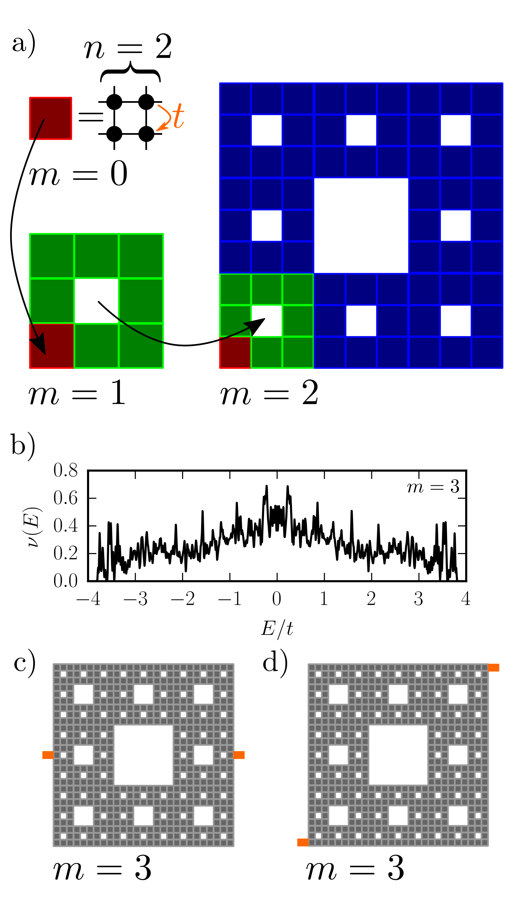
These experimental achievements motivate the theoretical investigation of complex 2D structures, with the aim of discovering novel transport and optical features which could enable or improve technological applications. In this work we present a theoretical study of the transport and optical properties of a 2DEG in a Sierpinski carpet (SC), which is a self-similar 2D structure falconer_book shown in Fig. 1. The self-similarity of the SC is mathematically quantified by the fact that its Hausdorff dimension falconer_book (i.e. a generalization of the topological dimension) is between one (a line) and two (a plane), which makes the SC a fractal mandelbrot_book .
While brownian motion and the heat diffusion equation on fractal geometries have been extensively studied in the literature diffusionfractals ; kusuoka , the transport and optical properties of electrons roaming on such complicated geometrical structures have comparatively received less attention. More precisely, some analytical chakrabarti_jpcm_1996 ; groth_prl_2008 and numerical liu_prb_1999 ; lin_prb_2002 ; jana_physicab_2010 ; song_apl_2014 studies of the conductance of electrons in Sierpinski fractals have appeared in the literature. We are instead unware of studies of the optical properties of electron systems in fractals, with the exception of an experimental work gourley_apl_1993 on a one-dimensional potential realized by growing a fractal sequence of quantum wells in (Al,Ga)As heterostructures.
In this work we show that the conductance of a 2DEG on a SC can reach the maximum value allowed by the number of open channels in the leads, depending on the lead positions and their widths, and it displays fractal fluctuations ketzmeric_prb_1996 ; taylor_book_2003 as a function of energy, in the absence of a magnetic field. We show that extended states, which are responsible for large conductance values, are quite robust to elastic disorder. Finally, we calculate the real part of the optical conductivity, which turns out to be much larger than and highly structured up to a photon energy of the order of , where is the hopping amplitude.
We hasten to stress that the problem at hand is very different from that of a quantum particle displaying a self-similar spectrum. Such problems are very well studied in physics, a paradigmatic example being that of the Hofstadter butterfly spectrum hofstadter_prb_1976 displayed by an electron moving in 2D under the combined effect of a periodic potential and a perpendicular magnetic field. Finally, we are not interested in the distribution of eigenvalues and nature of the corresponding eigenstates of electrons in plane fractals, which have been studied in great detail rammal_prl_1982 ; domany_prb_1983 ; rammal_prbr_1983 ; wang_prb_1995 ; hernando_arxiv_2015 . Rather, our aim is to unveil fundamental dc and ac transport characteristics, which can be measured with current technology.
Model and methods.—We describe a 2DEG in a SC by means of a single-orbital tight-binding Hamiltonian of the form
| (1) |
This describes electrons with spin hopping between the nearest-neighbor sites of a SC with Hausdorff dimension , as explained in Fig. 1. With reference to Fig. 1, each discretized SC sample is characterized by two integers, . In this work , while varies from to . The Hamiltonian (1) is particle-hole symmetric and the spectrum of eigenvalues extends from to for a bandwidth equal to .
The hopping parameter is used below as unit of energy. Nanopattering a SC on the surface of semiconductor hosting a high mobility 2DEG is expected singha_science_2011 ; gibertini_prbr_2009 ; desimoni_apl_2010 to yield of the order of a few meV, while protocols based on STM manipulation gomes_nature_2012 are expected to yield . For the sake of simplicity, we ignore magnetic fields and electron-electron interactions, which are expected to lead to very interesting quantitative and qualitative effects that will be the subject of future works.
The conductance and wavefunction calculations are performed by using kwant groth_2014 . In this toolkit, wavefunction matching is implemented to compute the wavefunctions in the scattering region and the scattering matrix for an incoming propagating mode and an outgoing mode . The conductance between the left lead L and the right lead R is given by the Landauer formula
| (2) |
The density of states (DOS) and optical conductivity are calculated by using the tight-binding propagation method (TBPM) yuan_prb_2010 ; yuan_prb_2011 . Since TBPM does not involve diagonalization of matrices, both CPU time and memory cost grown linearly with the sample size, allowing calculations with up to sites.
In TBPM, the DOS is obtained by the following Fourier transform hams_prb_2000 ; yuan_prb_2010 ; yuan_prb_2011
| (3) |
where the initial state is a superposition of localized orbitals with complex random coefficients and the wave propagation is performed numerically by using the Chebyshev polynomial algorithm. Our results for the DOS of a SC are reported in Fig. 1b). We have checked that the function rapidly converges for a fixed value of and increasing : for example, results for the and SCs (not shown) are nearly indistinguishable over the entire bandwidth.
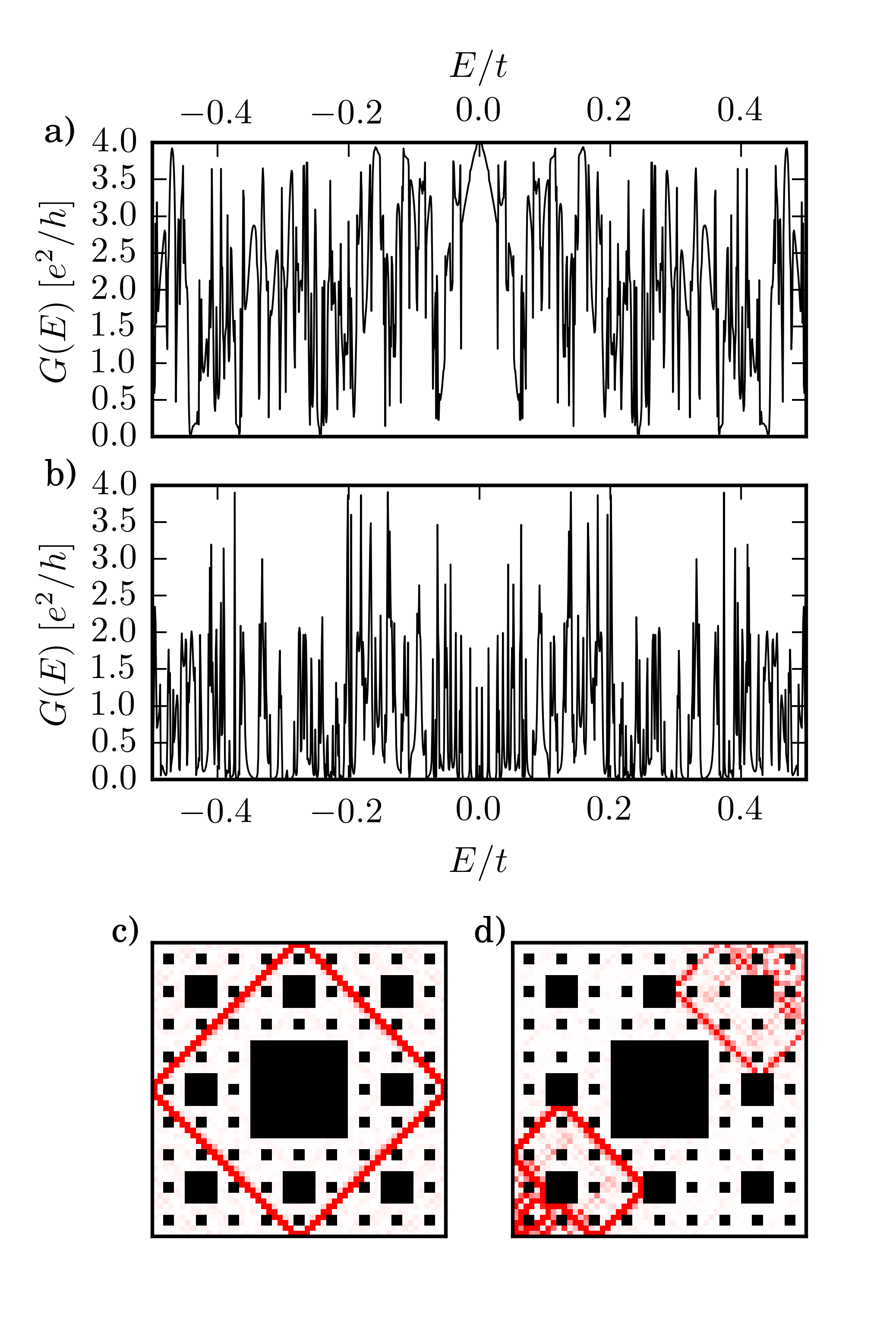
Quantum transport and fractal conductance fluctuations.—We have calculated the energy dependence of the two-terminal conductance of the tight-binding model (1), for two different lead configurations, as in Figs. 1c) and d).
A summary of our main results for a SC is reported in Fig. 2. In panel a) we clearly see that the two-terminal conductance is equal to for , where a conductive extended state is present chakrabarti_jpcm_1996 . This is because for the two leads positioned as in Fig. 1c), electrons of a given spin injected on the left side of the sample can reach the right side by following two equivalent paths, Fig. 2c), each carrying a conductance quantum, without being backscattered by the inner holes of the SC. On the other hand, as we can see from panel b), the sample can be insulating (i.e. ), at the same energy when probed with the leads positioned as in Fig. 1d).
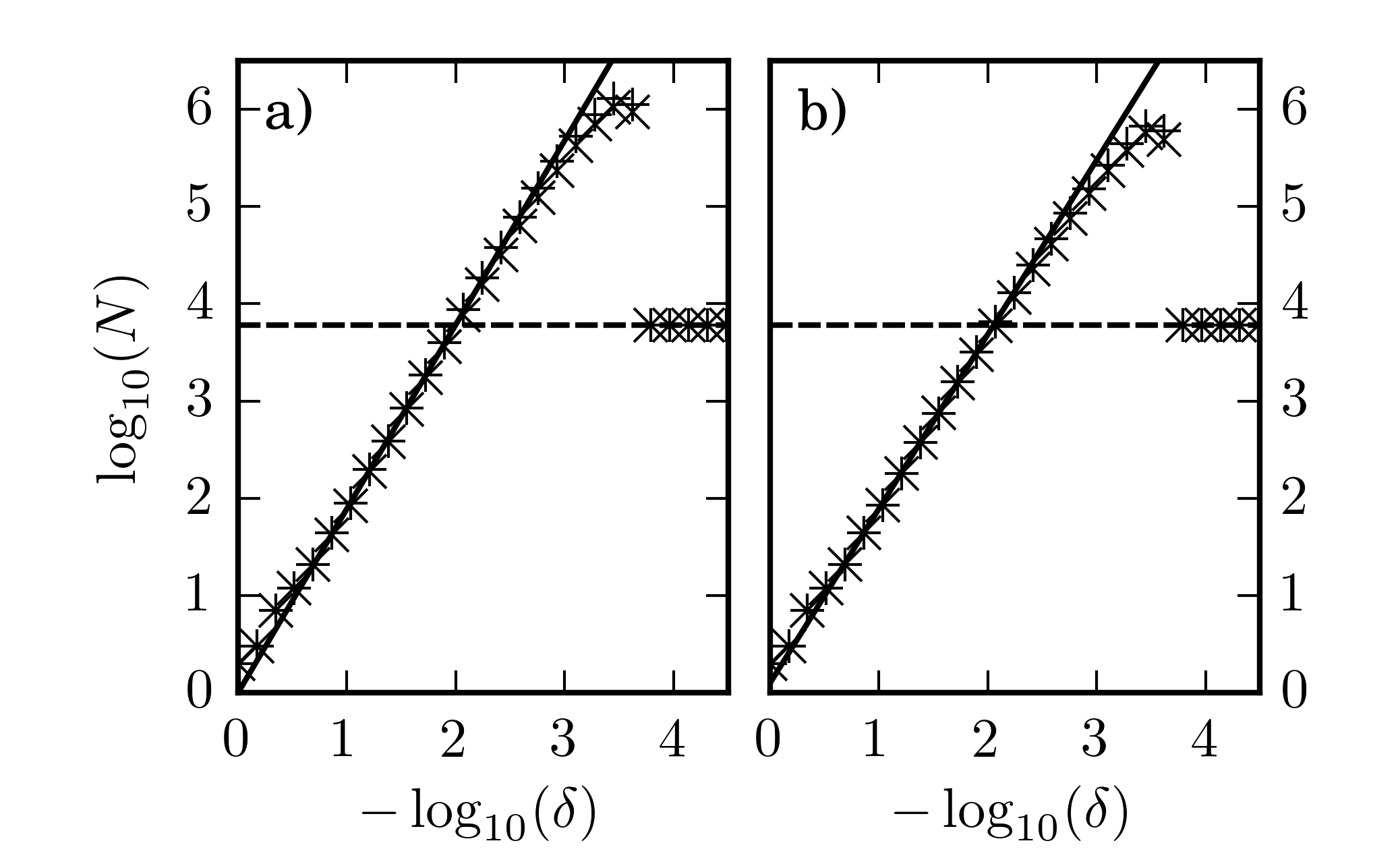
Data in Fig. 2 display also wild fluctuations. Such conductance fluctuations (CFs) can be quantitied by using a box-counting (BC) algorithm guarneri_pre_2001 . This counts the number of squares of size , which is necessary to continuously cover the graph of (in units of ) rescaled to a unit square. In general, points in the plane are expected to fall in three distinct regions. For large values of , the squares are too large to distinguish the features of the graph and grows slowly as decreases. For very small values of , the squares are so small that they resolve the single points in the set of data belonging to the CF graph: in this case is expected to saturate to the number of points in the energy mesh where is evaluated. Finally, there is an intermediate region (usually called “scaling region”) where scaling is linear in the log-log plane, i.e. where . The slope in the scaling region is the BC estimate of the Hausdorff dimension of the CFs.
In Fig. 3, we show the results of the BC algorithm for the CFs of two SC samples with (slightly) different Hausdorff dimensions, obtained by changing and in the iterative geometrical construction illustrated in Fig. 1a). Results do not depend on the spatial arrangement of the leads. The analyzed CFs clearly show fractal behavior over a scaling region of more than two orders of magnitude. Fractal CFs emerge ketzmeric_prb_1996 in the problem of phase-coherent ballistic transport and in the presence to strong quantum localization guarneri_pre_2001 . Indeed, in the SC transport problem, almost all wavefunctions are localized domany_prb_1983 [see e.g. Fig. 2d)] and do not contribute to transport (even in the absence of elastic disorder) due to scattering of electrons against the inner holes.
Finally, we note that the value of extracted from our numerical analysis is in excellent agreement with the Hausdorff dimension of the corresponding SC sample footnote_dimension . It is remarkable that the analysis of CFs carries information on the sample geometry, down to very small length scales.
Fig. 4 shows that the conductance of the 2DEG in a SC is robust with respect to both localized [panel a)] and smooth [panel b)] elastic disorder.
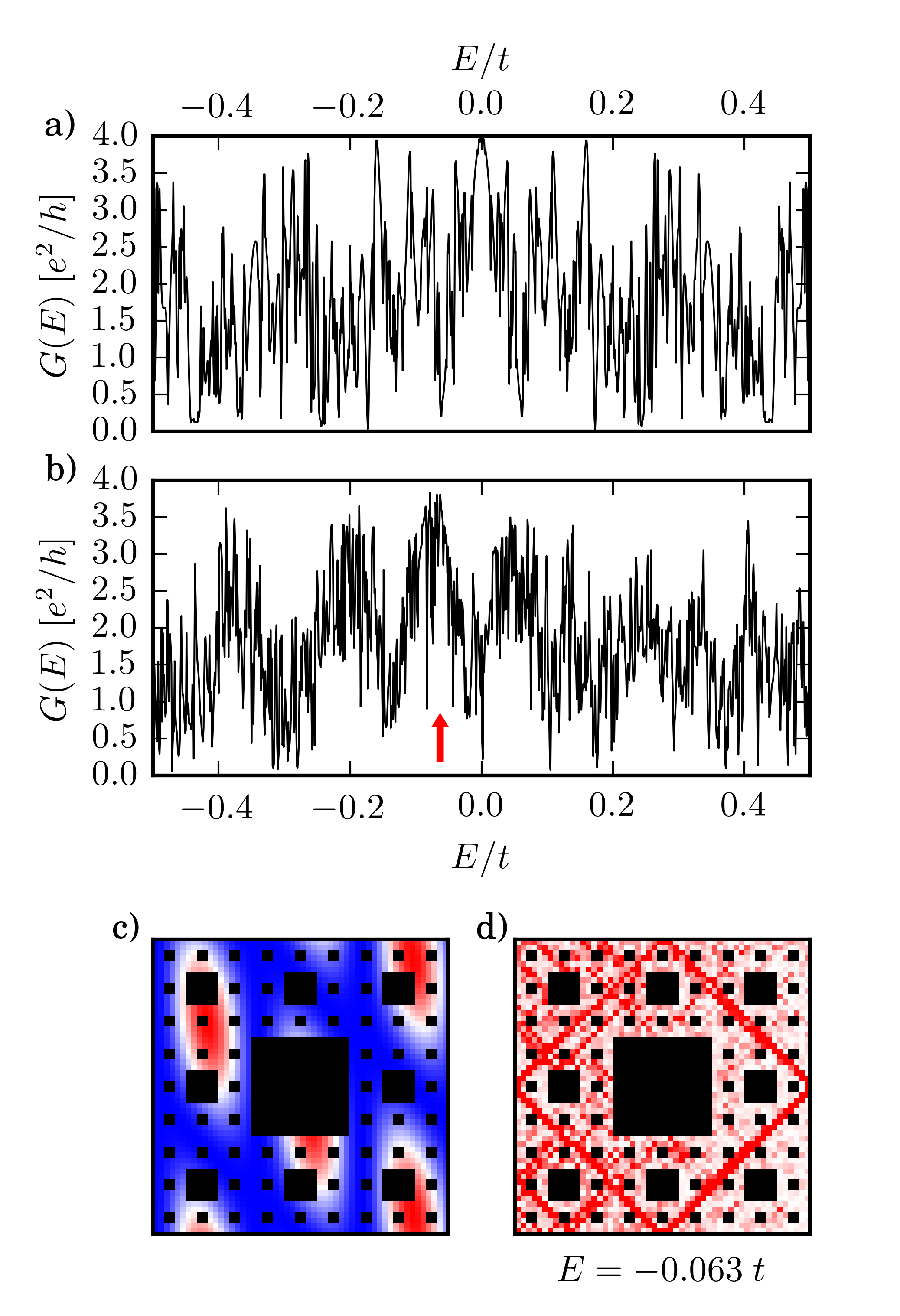
The impact of a single-site vacancy—located on the highly-conductive path through the bulk of the SC displayed in Fig. 2c)—is shown in Fig. 4a). We see that, despite such a strong, localized disorder source, still reaches its maximum value at . The impact of a smooth disorder potential,
| (4) |
which varies on an energy scale equal to of the hopping amplitude, is shown in Fig. 4b). The spatial variations of are reported in Fig. 4c), while the fate of the highly-conductive bulk path shown in Fig. 2c) is illustrated in Fig. 4d).
Optical conductivity.—We have calculated the optical conductivity from the Kubo formula for the current response function to a uniform time-dependent vector potential. In the TBPM, this is calculated (omitting the Drude contribution at ) from yuan_prb_2010 ; yuan_prb_2011 :
| (5) | |||||
where is the sample area, is the inverse temperature, is the Fermi-Dirac distribution operator, and is the current operator in the Heisenberg picture of the time evolution.
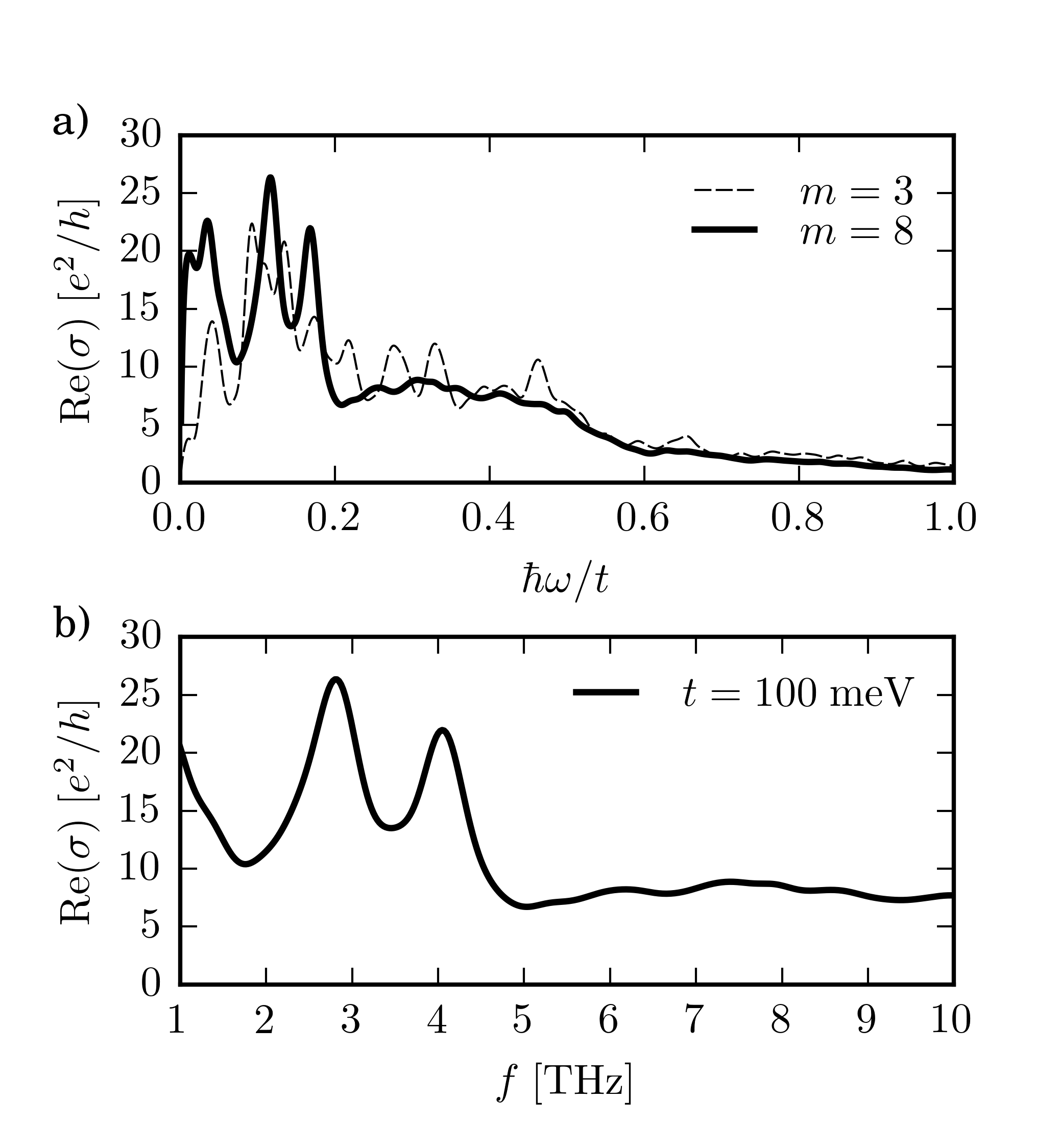
Fig. 5a) shows that the dependence of the absorption spectrum (in units of ) on the photon energy (in units of ). This quantity is evaluated at a finite but small temperature (specifically, ) and for two SC samples, i.e. and . By looking at the difference between at (not shown) and (and fixed temperature), we conclude that the data shown for represent the result. We note that the optical absorption spectrum features three distinct behaviors. For photon energies , absoption is very large, with , peaking at . The peak value is quite sensitive to the value of in a SC: for example, this peak reaches in a SC. For photon energies , features a plateau at a value which is intermediate between and . Finally, an exponential tail with kicks in for .
For a choice of the hopping amplitude (which is the expected value for a SC realized by STM manipulation gomes_nature_2012 ), the absorption of the SC vanishes in the visible range of the electromagnetic spectrum and it is of the order of in the infrared. For photon frequencies spanning the range the real part of the optical conductivity is very large, much larger than , and displays a sequence of molecular resonances (whose smoothness is controlled by temperature).
Summary.—In this work we have carried out extensive computer simulations of the conductance and optical absorption spectrum of a two-dimensional electron gas roaming on a prototypical plane fractal, the Sierpinski carpet. We have demonstrated that the conductance is sensitive to the spatial location of the leads and that it displays fractal fluctuations whose dimension is compatible with the Hausdorff dimension of the sample. Due to the presence of a massive number of localized eigenstates, the optical absorption spectrum turns out to display sharp molecular peaks at low photon energies, which may pave the way for applications in sensing and plasmonics.
Acknowledgements.
This work was supported by the European Research Council Advanced Grant program (contract 338957) (S.Y. and M.I.K.) and by the Italian Ministry of Education, University, and Research (MIUR) through the program “Progetti Premiali 2012” - Project ABNANOTECH (A.T. and M.P.). Support by the Netherlands National Computing Facilities foundation (NCF) is gratefully acknowledged. We gratefully acknowledge Luigi Ambrosio and Fabio Taddei for useful discussions, and Carlo Beenakker for very useful correspondence.References
- (1) M. Polini, F. Guinea, M. Lewenstein, H.C. Manoharan, and V. Pellegrini, Nature Nanotech. 8, 625 (2013).
- (2) A. Singha, M. Gibertini, B. Karmakar, S. Yuan, M. Polini, G. Vignale, M.I. Katsnelson, A. Pinczuk, L.N. Pfeiffer, K.W. West, and V. Pellegrini, Science 332, 1176 (2011).
- (3) K.K. Gomes, W. Mar, W. Ko, F. Guinea, and H.C. Manoharan, Nature 483, 306 (2012).
- (4) M.C. Rechtsman, J.M. Zeuner, Y. Plotnik, Y. Lumer, D. Podolsky, F. Dreisow, S. Nolte, M. Segev, and A. Szameit, Nature 496, 196 (2013).
- (5) G. Jotzu, M. Messer, R. Desbuquois, M. Lebrat, T. Uehlinger, D. Greif, and T. Esslinger, Nature 515, 237 (2014).
- (6) F.D.M. Haldane, Phys. Rev. Lett. 61, 2015 (1988).
- (7) M. Gibertini, A. Singha, V. Pellegrini, M. Polini, G. Vignale, A. Pinczuk, L.N. Pfeiffer, K.W. West, Phys. Rev. B 79, 241406(R) (2009).
- (8) G. De Simoni, A. Singha, M. Gibertini, B. Karmakar, M. Polini, V. Piazza, L.N. Pfeiffer, K.W. West, F. Beltram, and V. Pellegrini, Appl. Phys. Lett. 97, 132113 (2010).
- (9) C.-H. Park and S.G. Louie, Nano Lett. 9, 1793 (2009).
- (10) L. Nádvorník, M Orlita, N.A. Goncharuk, L Smrčka, V Novák, V. Jurka, K. Hruška, Z. Výborný, Z.R. Wasilewski, M. Potemski and K. Výborný, New J. Phys. 14, 053002 (2012).
- (11) S. Goswami, M.A. Aamir, C. Siegert, M. Pepper, I. Farrer, D.A. Ritchie, and A. Ghosh, Phys. Rev. B 85, 075427 (2012).
- (12) W.H. Evers, B. Goris, S. Bals, M. Casavola, J. de Graaf, R. van Roij, M. Dijkstra, and D. Vanmaekelberghet, Nano Lett. 13, 2317 (2013).
- (13) K.J. Falconer, The geometry of fractal sets (Cambridge University Press, Cambridge, 1985).
- (14) B.B. Mandelbrot, The fractal geometry of nature (W.H. Freemand and Company, New York, 1983).
- (15) S. Havlin and D. Ben-Avraham, Adv. Phys. 36, 695 (1987); M.B. Isichenko, Rev. Mod. Phys. 64, 961 (1992).
- (16) S. Kusuoka, Diffusion processes in nested fractals, in Statistical mechanics and fractals, Lect. Notes in Math. 1567 (Springer-Verlag, Berlin, 1993).
- (17) A. Chakrabarti, J. Phys.: Condens. Matter 8, 10951 (1996).
- (18) C.W. Groth, J. Tworzydło, and C.W.J. Beenakker, Phys. Rev. Lett. 100, 176804 (2008).
- (19) Y. Liu, Z. Hou, P.M. Hui, and W. Sritrakool, Phys. Rev. B 60, 133444 (1999).
- (20) Z. Lin, Y. Cao, Y. Liu, and P.M. Hui, Phys. Rev. B 66, 045311 (2002).
- (21) S. Jana, A. Chakrabarti, and S. Chattopadhyay, Physica B 405, 3735 (2010).
- (22) Z.-G. Song, Y.-Y. Zhang, and S.-S. Li, Appl. Phys. Lett. 104, 233106 (2014).
- (23) P.L. Gourley, C.P. Tigges, R.P. Schneider Jr., T.M. Brennan, B.E. Hammons and A.E. McDonald, Appl. Phys. Lett. 62, 1736 (1993).
- (24) R. Ketzmeric, Phys. Rev. B 54, 10841 (1996).
- (25) R. Taylor, R. Newbury, A. Micolich, M. Fromhold, H. Linke, G. Davies, J. Bird, T. Martin, and C. Marlow, A review of fractal conductance fluctuations in ballistic semiconductor devices, in Electron transport in quantum dots, edited by J.P. Bird (Kluwer Academic Publishers, 2003).
- (26) D.R. Hofstadter, Phys. Rev. B 14, 2239 (1976).
- (27) R. Rammal and G. Toulouse, Phys. Rev. Lett. 49, 1194 (1982).
- (28) E. Domany, S. Alexander, D. Bensimon, and L.P. Kadanoff, Phys. Rev. B 28, 3110 (1983).
- (29) R. Rammal, Phys. Rev. B 28, 4871(R) (1983).
- (30) X.R. Wang, Phys. Rev. B 51, 9310 (1995).
- (31) A. Hernando, M. Šulc, and J. Vaníček, arXiv:1503.07741.
- (32) C.W. Groth, M. Wimmer, A.R. Akhmerov, and X. Waintal, New J. Phys. 16, 063065 (2014).
- (33) S. Yuan, H. De Raedt, and M.I. Katsnelson, Phys. Rev. B 82, 115448 (2010).
- (34) S. Yuan, R. Roldán, H. De Raedt, and M.I. Katsnelson, Phys. Rev. B 84, 195418 (2011).
- (35) A. Hams and H. De Raedt, Phys. Rev. E 62, 4365 (2000).
- (36) I. Guarneri and M. Terraneo, Phys. Rev. E 65, 015203(R) (2001).
- (37) The Hausdorff dimensions of the SCs used to produce the results in Figs. 3a) and b) differ by only . To further corroborate the conjecture one needs to carry out a more detailed data analysis in which SCs with larger values of are used. This lowers the fractal dimension and can help finding deviations from the conjecture . Such a detailed numerical investigation requires the simulation of large samples, which is quite demanding, and lies outside the scope of the present work.