Improved Efficiency of Plasmonic Tin Sulfide Solar Cells
Abstract
Solar cells with the structure ITO-PEDOT:PSS-Ag:SnS-Al were fabricated with the active layer of tin sulphide with silver nano-particles (Ag:SnS) grown by thermal co-evaporation. To understand the influence of the silver nanoparticles on the energy conversion process, various cells with varying active layer thicknesses were compared. Results showed that the Ag nanoparticles act as scattering centers, resulting in longer optical path lengths for incident light. This in turn results in more charge carriers being generated and thus enhances the efficiency of the structure as compared to the pristine ITO-PEDOT:PSS-SnS-Al structure. The plasmonic solar cells of SnS showed an improvement of more than 40%. The results are encouraging and suggests more concerted effort needs to be made on SnS.
pacs:
71.20.Ps, 84.60.Jt, 75.50.TtPresent commercial solar cells are silicon wafer based with standard efficiency around 24.7%. silicon However, using the single crystal wafers cut to micro-meter thicknesses, increases the cost and makes utilization of solar energy economically unattractive. Researchers hence have started looking into organic organic1 ; organic2 and inorganic cds ; arbele materials in thin film state either in amorphous or polycrystalline state. amp ; poly The hope is to increase efficiency at a lower cost, effectively decreasing the energy conversion cost. The inorganic solar cells have not matched the efficiency of Silicon wafer solar cells as yet, with the best efficiency reported at 16.5% for Cadmium Telluride (CdTe) cdte film solar cells. However, with concerns on the toxicity of tellurium used, search has moved to other inorganic materials such as Tin Sulphide (SnS) reddy ; david and lead sulphide (PbS). pbs
The basic idea of solar cells are to absorb photons and generate charge carriers within the junction which should readily separate and reach their respective electrodes without recombination. To improve efficiency one requires a good absorbing material for the photo-active layer. This can be achieved either by using an active layer of good absorbance or increase its thickness. david However, the thickness of the layer is limited by the carrier diffusion length, i.e. the thickness of the active layer should always be less than the carrier diffusion length. atwater If the thickness of the active layer is larger than the carrier diffusion length, the carriers would recombine before being collected at the electrodes. This would reduce the current in the external circuitry and hence diminish the performance of the cell. Also, increasing the dimension of the absorber layer would raise the cost of the device. Selection of the second layer with opposite charge carriers (n or p type) to that of the semiconducting nature of the photo-active layer (p or n type) also plays an important role. The selection is made in view of matching the conduction and valence energy levels of the two layers such that the separation of the generated charge carriers is encouraged.
To increase the absorbance of the active layer without increasing the thickness, researchers are now investigating effects of embedding metal nanoparticles within the active layer. When light is incident on the metal/dielectric or a metal/semiconductor interface, it gives rise to collective oscillation of electrons known as “Surface Plasmon Resonance (SPR)”. spr At this particular resonance frequency, the nanoparticles either effectively absorbs light or scatters it. spr1 The amount of light scattered or absorbed depends on the size of the metal nanoparticles. spr1 ; spr2 Solar cells that use metal nano-clusters are called plasmonic solar cells. Derkacs et al. derkacs fabricated thin film amorphous Silicon solar cells containing Au nanoparticles and obtained an 8.3% increase in the conversion efficiency, while Schaadt et al. schaadt reported an enhancement of 80% when Au nanoparticles were incorporated in crystalline Silicon solar cells. Recently, Pillai et al. pillai reported a 30% enhancement in absorption in crystalline Silicon solar cells including Ag nanoparticles. Similar, studies were also carried out on other semiconductor solar cells as well. Konda et al. konda reported a significant enhancement in the photo-current for n-CdSe heterojunction solar cells containing Au nanoparticles. Stenzel et al. stenzel reported an improvement in photo-current by a factor of 2.7 when Au or Cu nanoparticles were embedded into ITO-Copper Phthalocyanine-In structures. Similar studies have been made in organic solar cells too, org1 ; org2 however till date, this plasmonic enhancement approach has not seen in SnS thin films. Thus, it would be interesting to see if the formation of LSPR improves the efficiencies of SnS solar cells.
SnS based solar cells today have very low conversion efficiency (at best 2% prasert ). Various research groups hence have focused on the factors that can improve the efficiency of SnS solar cells david ,ghosh ; noguchi . While majority of research try to address issue of selecting an appropriate companion ‘p’ or ‘n’-layer, ristov ; alex few groups have focused on improving the absorption of the photo-active SnS layer, david by varying the thickness, david or as in the stray example by embedding metal clusters within the film thickness ristov (However, it must be noted that Ristov et al did not talk of SPR in their work).
Tan et al tan in 2010 reported a solar cell structure based on quantum dots with PEDOT:PSS on ITO substrate. Both the PEDOT:PSS and layers were fabricated by spin-coat technique. We were able to fabricate this solar cells by thermally evaporating SnS on PEDOT:PSS-ITO acting as the p-type layer. We shall henceforth refer to this structure (ITO-PEDOT:PSS-SnS-Al) as the pristine solar cell. By modeling the solar cell as a single diode circuit, the cell parameters such as series resistance (), shunt resistance (), open circuit voltage (), Fill Factor (FF), ideality factor (n) and efficiency () were determined. In terms of these parameters, we were able to identically reproduce the solar cell reported by Tan et al tan with a maximum efficiency of 0.21% for a cell whose SnS film thickness was 800 nm and grain size around 17.7 nm. solarpaper
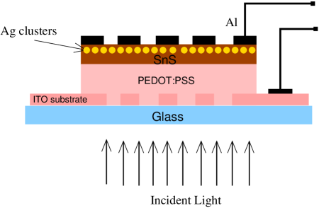
To increase the efficiency of these solar cells, we decided to fabricate plasmonic solar cells of SnS using 20 nm silver nano-particles. Fig 1 shows modifications made in our pristine solar cell device which incorporates oblate metal nano-particles of Ag residing at the surface of SnS film away from SnS/PEDOT:PSS junction. This article reports the performance of our plasmonic solar cells and compares its parameters with those of pristine SnS solar cells.
I Experimental Details
Solar cell structures of n-SnS:Ag/PEDOT:PSS were fabricated on etched Indium Tin Oxide (ITO) substrates of low resistivity (/sq). A 200 nm layer of aqueous solar grade PEDOT:PSS (1.3 %) was spin coated on the substrates. Followed by this, composite thin films of Tin sulfide (SnS) and silver (Ag) were grown on the PEDOT:PSS layer. The films were grown at room temperature by thermal evaporation technique using Hind Hi-Vac (12A4D) coating unit at vacuum better than Torr. Before evaporation, pellets were made by mixing SnS powder and Ag nano-powder. The SnS powder (99.99 % pure) was provided by Himedia (Mumbai) and the Ag nano-powder was provided by Nanoshel (USA). For mixing, the (mass) ratio of SnS:Ag taken was in a proportion of 2:1. The thickness of the composite films were measured using Veeco’s Dektak Surface profiler (150) on films grown simultaneously on glass substrates. Finally, Aluminum electrodes were deposited by thermal evaporation using standard masks. The thicknesses of the SnS:Ag composite films were varied while that of the spin coated PEDOT:PSS was maintained fixed.
The structural characterizations of the SnS films were done using a Bruker D8 diffractometer at an operating voltage of 40 KV in the mode with Cu target giving X-Ray of . The current-voltage (J-V) measurements were done with a computer monitored Keithley 2400 source meter unit. A solar simulator of , Air Mass (AM) 1.5 spectrum was used as illumination source. The measurements were made with light incident from the ITO side.
II Results and discussion
In our previous study jap we showed that Ag nano-clusters embedded in SnS acts as center for light scattering thus increasing the optical path length of light within the active layer. As stated, this is expected to increase the efficiency of the solar-cell. In the following passages we investigate this and compare the photo-voltaic parameters of our plasmonic-device with pristine SnS solar cells.
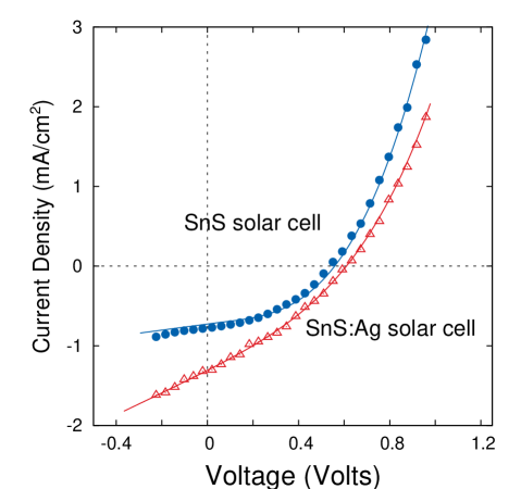
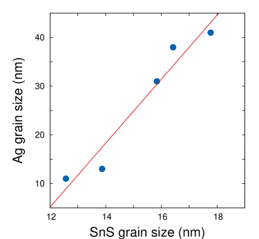
Fig 2 compares the J-V characteristics of SnS solar cell with that of a plasmonic SnS:Ag solar cell. The curves selected are of cells with 800 nm thick photo-active layer and are representative of all measurements made. An increase in the efficiency of the plasmonic SnS:Ag cell can be judged by the increase in area enclosed by the J-V curve in the forth quadrant. In our study on pristine cells, solarpaper we had discussed the properties as a function of SnS grain size. However, the analysis of our previous work jap suggests that Ag nanoparticle’s efficiency to scatter light into the dielectric SnS background depends on the Ag nanoparticles’s grain size, it would be necessary to compare conversion efficiencies as a function of a parameter on which both Ag and SnS grain size would depend on. Fortunately, both SnS grain size jos and Ag nanoparticle’s grain size (fig 3) show a linear trend with the active layer’s thickness (within region of experimental interest).
Hence, in fig 4, we plot the efficiency of SnS thin film solar cells and SnS:Ag plasmonic Solar cells as a function of the active layer’s thickness. The conversion efficiency increases with increasing film thickness. In fact, for an active layer of thickness 800nm, the conversion efficiency of the device is enhanced by 42 when the Ag nanoparticles were introduced in SnS films. The increase (rate) in efficiency with film thickness can not be explained merely by the insignificant variation in absorbance with film thickness reported. tsf ; jos

The increase in efficiency is hence related to the scattering from Ag nanoparticles. Larger metal nanoparticles results in more scattering. This increases the optical path of incident light within the cell leading to more charge carriers being released. A relook at fig 2 shows that the increase in efficiency of Ag:SnS solar cell is due to the increasing short-circuit current density, (point at which J-V curve cuts the ‘Y’-axis) with marginal or no increase in open circuit voltage, (point at which J-V curve cuts the ‘X’-axis). Fig 5 shows a plot between Ag nanoparticle’s grain size and . The trend confirms that more charge carriers are generated with increasing Ag nanoparticle’s size. A maximum enhancement of 27 in the photo-current was measured in SnS:Ag solar cells as compared to the pristine cells.

III Conclusion
Plasmonic solar cells of SnS were fabricated by co-evaporation of silver metal during the fabrication of ITO-PEDOT:PSS-Ag:SnS-Al structures. A substantial increase in the conversion efficiency of the device was observed as compared to the pristine (non-plasmonic) ITO-PEDOT:PSS-SnS-Al structures. The increase in efficiency is shown to be due to increasing photo-current generated due to increase in light scattering within the cell due to the Ag nanoparticles. The results are promising considering that we now can manipulate the inorganic, non-toxic SnS solar devices for higher efficiency.
References
- (1) Wang A., Zhao J. and Green M.A., 24 efficient silicon solar cells, Appl. Phys. Lett. 57 (1990) 602.
- (2) Erb T., Zhokhavets U., Gobsch G., Raleva S., Stuhn B., Schilinsky P., Waldauf C. and Brabec C.J., Correlation Between Structural and Optical Properties of Composite Polymer/Fullerene Films for Organic Solar Cells, Adv. Funct. Mater., 15 (2005) 1193.
- (3) Yu G., Gao J., Hummelen J.C., Wudl F., and Heeger A.J., Polymer Photovoltaic Cells: Enhanced Efficiencies via a Network of Internal Donor-Acceptor Heterojunctions, Science, 270 (1995) 1789.
- (4) Wagner S., Shay J.L., Bachmann K.J., Buehler E., p−InP/n−CdS solar cells and photovoltaic detectors, Appl. Phys. Lett. 26 (1975) 22.
- (5) Aberle A.G., Thin Film Solar Cells, Thin Solid Films, 517 (2009) 4706.
- (6) Kriihler W., Amorphous Thin-Film Solar Cells, Appl. Phys. A, 53 (1991) 54.
- (7) Birkmire R.W. and Eser E., Polycrystalline thin film solar cells: Present Status and Future Potential, Annu. Rev. Mater. Sci., 27 (1997) 625.
- (8) Mohamed H.A.,Dependence of efficiency of thin-film CdS/CdTe solar cell on optical and recombination losses, J. Appl. Phys. 113 (2013) 093105.
- (9) Reddy K.T.R., Reddy N.K. and Miles R.W., Photovoltaic Properties of SnS based solar cells. Sol. Energy Mater. Sol. Cells 90 (2006) 3041.
- (10) Avellaneda D., Nair M.T.S., Nair P.K., Photovolatic structures using chemically deposited tin sulfide thin films., Thin solid films 517 (2009) 2500.
- (11) Piliego C., Protesescu L. , Bisri S.Z. , Kovalenkobc M.V., Loi M.A., 5.2 efficient PbS nanocrystal Schottky solar cell, Energy Environ. Sci. 6 (2013) 3054.
- (12) Atwater H.A. and Polman A.,Plasmonics for improved photovoltaic devices, Nature Materials, 9 (2010) 205.
- (13) Bohren C.F. and Huffman D.R., Absorption and Scattering of Light by Small Particles, John Wiley & Sons, Inc., New Yark (1983).
- (14) Catchpole K.R. and Polman A., Plasmonic solar cells, Optic. Express, 16 (2008) 21793.
- (15) P. K. Jain, K. S. Lee, I. H. El-Sayed, and M. A. El-Sayed, J. Phys. Chem. B 110, 7238 (2006).
- (16) Derkacs D., Lim S.H., Matheu P., Mar W., and Yu E.T., Improved performance of amorphous silicon solar cells via scattering from surface plasmon polaritons in nearby metallic nanoparticles, Appl. Phys. Lett., 89 (2006) 093103.
- (17) Schaadt D.M., Feng B., and Yu E.T., Enhanced semiconductor optical absorption via surface plasmon excitation in metal nanoparticles, Appl. Phys. Lett., 86 (2005) 063106.
- (18) Pillai S., Catchpole K.R., Trupke T., and Green M.A., Surface plasmon enhanced silicon solar cells, J. Appl. Phys., 101 (2007) 093105.
- (19) Konda R.B., Mundle R., Mustafa H., Bamiduro O., Pradhan A.K., Roy U.N., Cui Y., and Burger A., Surface plasmon excitation via Au nanoparticles in n-CdSe/p-Si heterojunction diodes, Appl. Phys. Lett., 91 (2007) 191111.
- (20) Stenzel O., Stendhal A., Voigtsberger K., Borczyskowski C.V., Enhancement of the photovoltaıc conversion efficiency of copper phthalocyanine thin film devices by incorporation of metal clusters, Sol. Energy Mater. Sol. Cells, 37 (1995) 337.
- (21) Rand B.P., Peumans P. and Forrest S.R., Long-range absorption enhancement in organic tandem thin- film solar cells containing silver nanoclusters, J. Appl. Phys., 96 (2004) 7519.
- (22) Morfa A.J., Rowlen K.L., Reilly III T.H., Romero M.J. and Lagemaat J.V.D, Plasmon-enhanced solar energy conversion in organic bulk heterojunction photovoltaics, Appl. Phys. Lett., 92 (2008) 013504.
- (23) Sinsermsuksakul P., Hartman K., Kim S.B., Heo J., Sun L., Park H.H., Chakrabotry R., Buonassisi, Gordon R.G., Enhancing the efficiency of SnS solar cells via band-offset engineering with a zinc oxysulfide buffer layer, Adv. Energy Mater. 102 (2013) 053901.
- (24) Ghosh B., Das M., Banerjee P., Das S., Fabrication of vacuum-evaporated SnS/CdS heterojunction for PV applications., Sol. energy Mater. Sol. Cells 92 (2008) 1099.
- (25) Noguchi H., Setiyadi A., Tanamora H., Nagatomo T., Omoto O., Characterization of vacuum-evaporated tin sulfide film for solar cell materials., Sol. Energy Mater. Sol. Cells, 35 (1994) 325.
- (26) Ristov M., Sinadinovski G., Mitreski M., Ristova M., Photovoltaic cells based on chemically deposited p-type SnS, Sol. Energy Mater. Sol. Cells 69 (2001) 17.
- (27) Stavrinadis A., Smith J.M., Cattley C.A., Cook A.G., Grant P.S., Watt A.A.R., SnS/PbS nanocrystal heterojunction photovoltaics, J. Nanotech. 21 (2010) 1.
- (28) Tan F., Qu S., Zeng X., Zhang C., Shi M., Wang Z., Jin L., Bi Y., Cao J., Wang Z., Hou Y., Teng F., Feng Z., Photovoltaic effect of tin disulfide with nanocrystalline/amorphous blended phases, Solid State Communications 150 (2010) 58.
- (29) Jain P. and Arun P., Photovoltaic performance of hybrid ITO/PEDOT:PSS/n-SnS/Al solar cell structure, (Submitted to J. Renew. Sustain. Energy).
- (30) Jain P. and Arun P., Localized surface plasmon resonance in SnS:Ag nano-composite films, J. Appl. Phys. 115 (2014) 204512.
- (31) Jain P. and Arun P., Parameters influencing the optical properties of SnS thin films, J. Semicond., 34 (2013) 093004-1.
- (32) Jain P. and Arun P., Influence of grain size on the band-gap of annealed SnS thin films, Thin Solid Films, 548 (2013) 241.