∎
Tel.: +1-919-660-5258
Fax: +1-919-660-5247
22email: jungsang@duke.edu
33institutetext: P. Maunz 44institutetext: Sandia National Laboratories, Albuquerque, N.M. 87123
Scalable Digital Hardware for a Trapped Ion Quantum Computer ††thanks: This work was supported by the Office of the Director of National Intelligence and Intelligence Advanced Research Projects Activity through the Army Research Office.
Abstract
Many of the challenges of scaling quantum computer hardware lie at the interface between the qubits and the classical control signals used to manipulate them. Modular ion trap quantum computer architectures address scalability by constructing individual quantum processors interconnected via a network of quantum communication channels. Successful operation of such quantum hardware requires a fully programmable classical control system capable of frequency stabilizing the continuous wave lasers necessary for trapping and cooling the ion qubits, stabilizing the optical frequency combs used to drive logic gate operations on the ion qubits, providing a large number of analog voltage sources to drive the trap electrodes, and a scheme for maintaining phase coherence among all the controllers that manipulate the qubits. In this work, we describe scalable solutions to these hardware development challenges.
Keywords:
Quantum computation Qubits Trapped ionspacs:
03.67.-a 03.67.Lx1 Introduction
Trapped ions exhibit many favorable properties for use as qubits Wineland1998 ; Blatt2008 , such as long coherence times Langer2005 , near perfect state preparation and readout Myerson2008 ; Noek2013 , and high fidelity qubit gate operations Benhelm2008 ; Brown2011 ; Ballance2014 . The Modular Universal Scalable Ion-trap Quantum Computer (MUSIQC) platform provides a scalable architecture where registers of ion qubits can be trapped in scalable surface electrode ion traps Merrill2011 ; Moehring2011 . Each quantum register must be capable of performing arbitrary quantum logic operations among the qubits in the register, as well as supporting the optical interface needed to communicate qubits between quantum registers through a photonic network Monroe2013 ; Monroe2014 .
Any ion trap quantum computer, and specifically the MUSIQC architecture Monroe2013 ; Monroe2014 , requires a wide range of classical hardware to drive the quantum operations needed for the computation. Scaling up from a small laboratory experiment to a large-scale processor will require scalable classical resources in addition to qubits. Here we present scalable hardware to perform some of the classical tasks required by an ion trap quantum computer. These tasks include: continuous wave (CW) laser frequency locking, frequency stabilization of pulsed laser beams for quantum logic gates, and low-noise digital-to-analog converter (DAC) systems for trapping and shuttling ions. We designed each of these systems to be inexpensive, compact, and extensible such that they can grow or be replicated to accommodate a much larger experiment. The techniques are developed for hyperfine qubit levels separated by approximately 12.6 GHz, where resonant laser beams at 369.5 nm and off-resonant Raman beams detuned 14–33 THz from the to levels are used to manipulate the qubits. Many of these techniques can be extended to hyperfine qubits in other ion species.
2 Offset frequency lock for CW laser stabilization
The narrow spectral linewidths (MHz) that are typical of atomic qubits and neutral atom experiments require lasers with high frequency specificity and stability. Current state-of-the-art laser systems that rely on the control of operating current and temperature are unable to sufficiently stabilize the frequencies of commercial laser diodes to meet these needs, so active locking to another frequency reference is often used. Commercially available vapor cells allow for easy stabilization of lasers addressing neutral atom transitions, but such a simple and inexpensive solution is not available to lasers addressing ion transitions (by virtue of their ionic nature), and other methods must be employed.
One approach to frequency locking an external cavity diode laser (ECDL) is to use a second laser, locked to a vapor cell at frequency (e.g. 780 nm for Rb vapor), and an optical cavity. The optical cavity is designed to support both and light at the desired ECDL frequency (e.g. 369.5 nm for ions). The optical cavity length is stabilized to while the cavity error signal is used to provide feedback to the piezo-controlled grating inside the ECDL, effectively transferring the vapor cell frequency reference to the ECDL. A second approach, where the ECDL is stabilized to the transitions of an ion plasma (for example, in a hollow-cathode lamp) can also provide the frequency stability necessary for trapped ion experiments Lee2014 . While both approaches can adequately stabilize the frequency of an ECDL for trapped ion experiments, scaling is a concern as they are expensive and cumbersome to implement, especially for a complicated experiment involving multiple lasers. Here we present a scheme that transfers the lock of a single master laser to multiple slave lasers with minimal hardware, complexity, and cost.
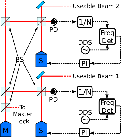
In this scheme (shown in Fig. 1), a portion of the slave’s output and a small amount of light from the frequency stabilized master laser are matched in mode shape and polarization, and overlapped on a photodiode (PD). The overlapped electric fields result in a beat note at the difference frequency between the master and slave lasers, which is detected by PD. The range of detectable beat note frequencies is limited by the PD bandwidth and is typically a few tens of MHz to several GHz. The beat note is amplified and compared to a reference signal (generated by a direct digital synthesizer (DDS) in our case) using a phase/frequency detection circuit. After appropriate filtering, the output of the circuit can be used as an error signal to provide feedback to the piezo-tunable grating and/or current of the slave ECDL using standard Pound-Drever-Hall control techniques Drever1983 . The frequency difference between the master and slave lasers is digitally programmable by the DDS frequency to be using a prescaler, as shown in Fig. 1.
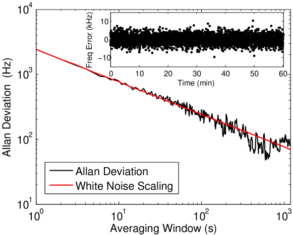
This solution is highly scalable as many slave lasers can be locked to a single master laser. The number of slave lasers that can be locked to a single master laser is limited by the total power of the master laser. In our system, a 369.5 nm ECDL, with an output power of 3.4 mW, serves as the master laser which is frequency stabilized to a hollow-cathode lamp Lee2014 . From the master laser, 600 W of power is used to lock 3 slave lasers at different offset frequencies (determined by the DDS frequency). We are currently capable of locking up to 8 slave lasers to a single master laser, which is more than enough to meet our current experimental demands. If necessary, this number could be pushed higher with further improvements in mode-matching, or with more specialized equipment. The beat note is detected by a high-speed response (2 GHz) photodiode (S9055, Hamamatsu), thus we are able to stabilize the master laser to the and have slave lasers stabilized to either the and resonances as necessary. From the Allan deviation of the beat note frequency for a slave 369.5 nm ECDL, we see that the beat note frequency noise is approximately white (Fig. 2).
The footprint and complexity of the lock is reduced significantly using this approach as each additional slave laser merely requires a beam splitter to overlap the two laser beams, a focusing lens, and a photodiode, all of which can easily fit on a small breadboard with beams delivered via optical fibers. Additionally, the cost to implement the offset lock is more than an order of magnitude smaller than the cost of alternative approaches such as an additional transfer cavity or a hollow-cathode lamp.
3 Digital optical frequency comb lock for Raman transitions
For trapped ion qubits, driving qubit transitions using optical fields is convenient as they can be tightly focused for the individual addressing of single ions in a closely packed linear chain of ions. Optical frequency combs from mode-locked lasers are ideal for this purpose due to their broad bandwidth (10 GHz to 100 THz) which can bridge the wide energy separation of atomic states, and tightly spaced comb teeth, which are separated by the laser repetition rate (), usually in the 50–1,000 MHz range Hayes2010 ; Islam2014 .
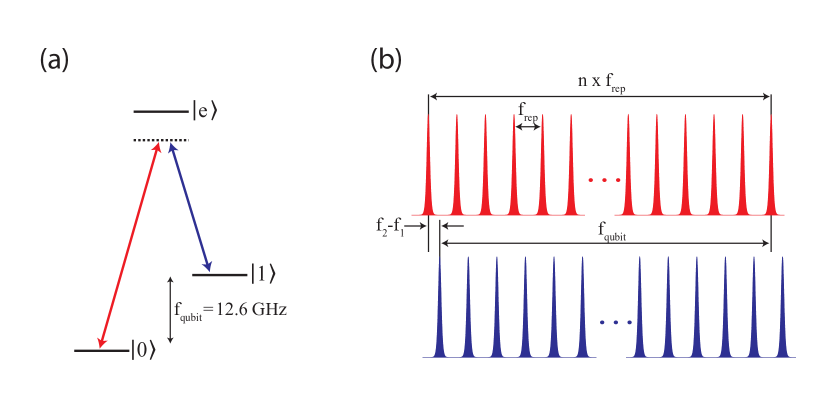
The magnetically insensitive hyperfine ground states of the ion serve as our qubit states with S and S, at a qubit frequency of 12.6 GHz. This system can be approximated as a three level system, shown in Fig. 3(a). Two-photon stimulated Raman transitions between qubit states and can be driven using two optical frequency combs Hayes2010 . Fig. 3(b) shows optical frequency combs generated from a single mode-locked laser where the relative offset between the two combs, , is introduced by an acousto-optic modulator (AOM). When the frequency difference is such that
| (1) |
where is an integer, an off-resonant two-photon Raman process induces the transition between and states through the virtual excited state . Because the Raman transitions are driven by the comb teeth pairs separated by exactly , it is sufficient to stabilize the relevant pair of comb teeth to each other, instead of stabilizing the absolute frequency or repetition rate of the laser output.
Thermal drifts and the vibration of mechanical parts in the laser cavity are among the main causes of drift in the laser repetition rate, which decreases gate fidelities by detuning the frequency comb pairs from . Stabilization of can be accomplished by directly stabilizing the laser cavity length; While this method provides sufficient stability and was used in previous experiments Mount2013 , the lock bandwidth is typically limited to the kHz range due to its reliance on piezo-translation of a relatively large mirror HayesThesis . This method requires access to the laser cavity, not available in many commercial lasers used in these experiments, and requires a stable microwave oscillator that filters near which can be costly. Our alternative approach is to measure the drift of by locking a digitally-controlled oscillator (such as a DDS) to the repetition rate signal using a digital phase-locked loop (PLL), and compute the driving frequency, , of the optical modulator to satisfy Eq. 1. We implement the lock digitally, using a proportional-integral (PI) controller implemented in a field programmable gate array (FPGA). The system provides a low-cost and scalable alternative to hardware-intensive analog methods and is a viable alternative when laser cavity access is limited.
3.1 Implementation
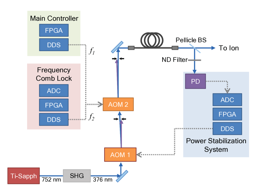
The optical frequency comb stabilization setup is shown in Fig. 4. A mode-locked titanium sapphire laser (centered at 752 nm, 2 ps FWHM pulse duration) is used to generate an optical frequency comb with comb teeth separation of 76 MHz. The laser output is frequency doubled via second harmonic generation (SHG) using a BiBO crystal (length 8 mm). The light from the SHG output (376 nm) is split into two approximately co-propagating frequency combs by driving an AOM with two frequencies: , controlled by the main experimental control FPGA and used to scan the detuning of the Raman beams in the experiments, and , used to stabilize the frequency difference between the pairs of comb teeth that drive the Raman transition. The co-propagating beam geometry ensures temporal overlap of the pulses at the ion.
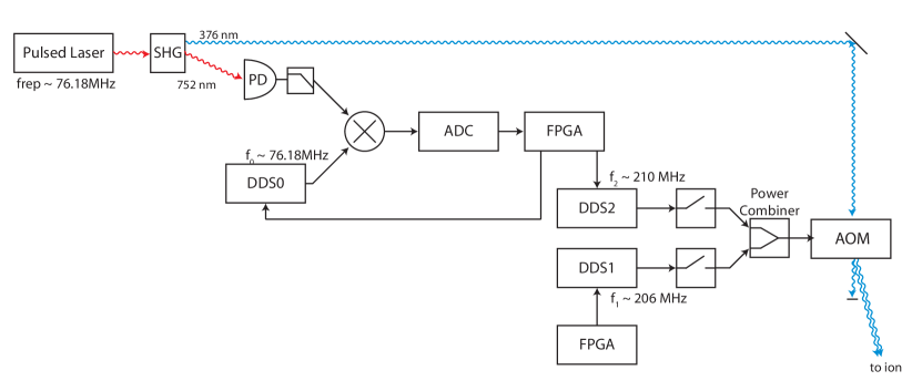
A small fraction of the laser output at the fundamental wavelength (752 nm) is incident on a photodiode (PD, S9055 Hamamatsu), and then amplified and low-pass filtered to attenuate the higher harmonics of . The filtered PD output is mixed with the amplified output of a DDS (DDS0, Analog Devices, AD9912, 4 Hz frequency resolution). The mixer output is low-pass filtered to eliminate the high frequency harmonics, while preserving the portion related to the frequency and phase difference, which provides the error signal for the PI controller in the PLL. Digitization of the error signal is performed by an analog-to-digital converter (ADC, Analog Devices AD7671, 16-bit resolution, 1 MSPS) and then read by the FPGA (Altera Cyclone II). The PI computation is performed in the FPGA which sets the frequency values of DDS0 () to track , and DDS2 () to satisfy Eq. 1. All DDSs share the same reference clock.
The lock operates as follows: a small change in , in time step k, results in a digitized error signal , where is the sampling interval, and and are the phases of the PD and DDS0 outputs, respectively. Given constants and , each time step a correction is made to where
| (2) |
This locks the frequency and phase of to via feedback control. Consequently, when drifts such that
| (3) |
is known, as the corresponding is set by the FPGA to match . The FPGA feeds-forward the value of the harmonic of to , so that
| (4) |
This maintains the equality in Eq. 1, and
| (5) |
allowing for stable qubit transitions as drifts. With MHz and GHz, .
3.2 Lock parameters
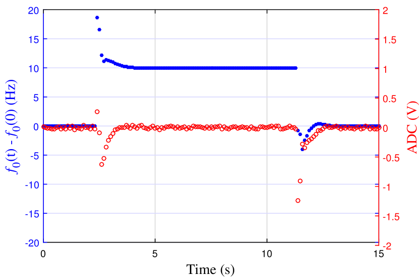
By examining the mixer output (error signal) on an oscilloscope, we determined a maximum rate of drift of Hz/s. To establish the optimal integral gain coefficient, , and the frequency difference detection sensitivity of our system, we replaced the PD output with another DDS, which was amplified to the same output power level and set to about the same frequency as the PD output. After enabling the lock with a proportional coefficient , the DDS frequency was changed abruptly, as shown in Fig. 5. The coefficient was chosen to provide a 50 Hz/s slew rate, sufficient for the lock to follow our expected 5 Hz/s rate of change. With the determined, to minimize noise we used the minimum proportional coefficient necessary to stabilize the lock.
3.3 Digital filtering
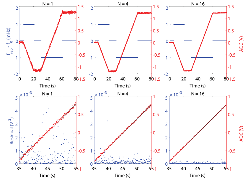
In our lock implementation, digital filters can be inserted without any hardware modification. A simple averaging filter was implemented where, upon receiving error signal samples at the maximum rate of 1 MSPS from the ADC, the PI loop proceeds using as the error signal. Fig. 6(a) shows the ADC readings where is again replaced with a DDS. The DDS is set to take finite frequency steps, similar to Fig. 5 with the system unlocked, at different values of . The ADC noise is clearly reduced by digital averaging as evidenced by the residuals of a simple linear regression, shown in Fig. 6(b). While averaging decreases the error signal noise, the locking bandwidth is also reduced. With no digital averaging, the locking bandwidth of the digital PI loop is limited to 1 MHz by the conversion speed of the ADC. With digital averaging, the lock bandwidth is reduced by .
3.4 Lock verification
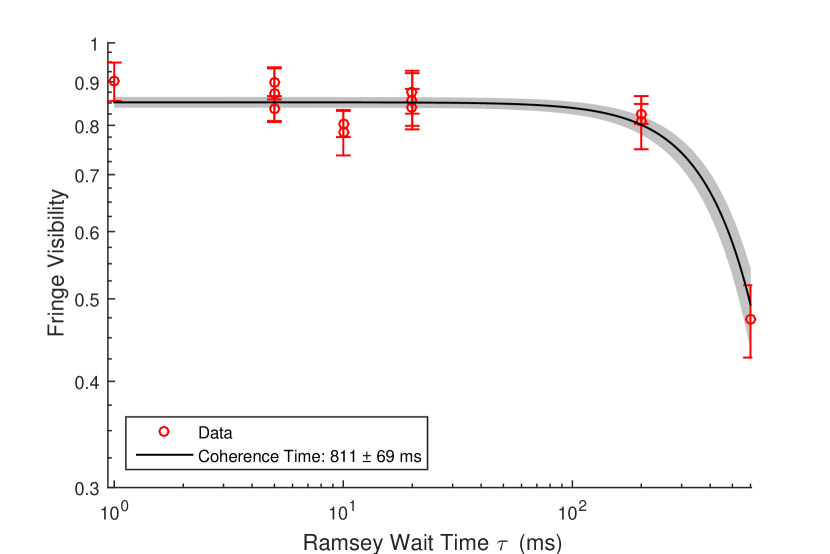
High fidelity qubit operations require that Raman beat notes stay coherent with the qubit frequency for the duration of the computation. To measure the coherence time, a Ramsey experiment was performed. First, the qubit is initialized into the state, followed by a pulse that rotates the qubit into a superposition state. After a wait time of , a second pulse, with a phase shift of with respect to the first pulse, is implemented followed by a measurement. This procedure is repeated for many values of resulting in a fringe. The fringe visibility indicates how well difference frequency of the Raman beams remains synchronized with the phase of the qubit.
Using the digital optical frequency comb lock we measure a coherence time of ms, shown in Fig. 7. The coherence time is determined by fitting the Ramsey fringe visibility versus to the Gaussian function exp(-), where is the coherence time. By directly stabilizing the cavity length in the same laser, we previously measured a coherence time of ms using a similar procedure Mount2013 .
3.5 Global synchronization
In a scalable quantum hardware system, it is crucial that the phase coherence of all classical fields that manipulate various parts of the system be maintained. In the case of Raman beams that drive quantum logic gates, the phase of the Raman beat notes must be maintained, in case there are multiple pairs of Raman beams driving quantum gates across the system. We ensure this by driving all the DDS controllers and microwave sources in the system from a single clock signal derived from an atomic standard. The relative phase difference between all of the RF and microwave control signals reaching the qubits must be calibrated (and stabilized) to operate a distributed quantum system such as MUSIQC.
4 Digital optical intensity lock
Intensity fluctuations of the Raman beams at the ion location result in the degradation of gate fidelities, and drifts in Rabi frequency and Stark shift calibrations. For high fidelity gates, control of the laser power at the ion location is critical. Here, we implement a power stabilization system using a PD, ADC, FPGA, and a DDS. As shown in Fig. 8, after the frequency combs exit the fiber, a small amount of collimated light is picked-off and placed on a PD. The PD signal is digitized by an ADC (AD7671) and relayed to the FPGA (Altera, Cyclone II). This provides the error signal for a PI feedback loop, similar to that used in Sect. 3.1. The FPGA actively stabilizes the power on the PD by controlling the amplitude of the DDS signal driving AOM 1. This implementation allows for gating of the PI loop by a digital trigger pulse, sent from the FPGA in our main controller. In most experiments the Raman beams must be turned on and off. A digital trigger allows the PD to be placed after the AOMs, closer to the ion, providing better intensity stabilization. In our experiments, we turn the Raman beams and PI loop on during the Doppler cooling cycle, allowing the power in the Raman beams to be stabilized before the experiment. Once the cooling cycle is complete, the feedback control is turned off, and we hold the final value of the AOM amplitude setting from the lock throughout the remainder of the experiment until the next cooling cycle. Using this sample and hold approach, slow intensity fluctuations due to beam pointing instability before the fiber are corrected.
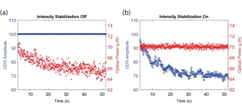
Figure 9 shows the impact of intensity stabilization. When the lock is turned off (constant DDS amplitude, as in Fig. 9a), the power delivered through the fiber drifts as monitored by the PD (sampled by the ADC). Once the locked is turned on, the DDS amplitude is adjusted to maintain constant optical power out of the fiber (Fig. 9b).
5 Next generation lock
We are developing a general-purpose 8-channel digital proportional-integral-differential (PID) control system to replace the PI loop implementations discussed in sections 2-4 and to be used for future locking tasks. It supports multiple user-selectable outputs for the lock, such as DC voltage through digital-to-analog converters (DACs) and frequency or amplitude of DDS signals, among others.
The PID logic is implemented on a Xilinx Spartan 6 FPGA, detailed in Fig. 10. The FPGA is mounted on a circuit board that also contains an 8-channel ADC (Analog Devices AD7608, 18-bit resolution, 200 ksps) and DACs (Texas Instruments DAC8568, 16-bit resolution) for each channel. The locking system can support eight PID locks concurrently, each with optional DC output, using the integrated DACs (66 kHz maximum update rate), or AC output, via an off-chip DDS (Analog Devices AD9912, 100 kHz maximum update rate). A Python graphical user interface (GUI) was designed for selection of locking parameters and real-time lock monitoring, with communication to the FPGA provided by a USB 2.0 link. Digital filtering, as in section 3.3, is available on each channel through an oversampling module that performs digital averaging of the error signal.
6 Digital to Analog Converter System
Historically, macroscopic 4-rod RF-Paul ion traps have been used for trapped ion quantum information experiments Turchette2000 ; Maunz2007 ; Benhelm2008 . However, in recent years surface-electrode ion traps have come into use, as they provide repeatable trap parameters and support increased complexity. The trapping potential is constructed from a sum of RF and DC components. In a surface-electrode ion trap, these fields are generated by applying voltages to microfabricated metal electrodes located on a planar surface at a distance on the order of m from the ions. The voltages applied to these electrodes can be modulated to shuttle the ions along the trap axis or split and re-combine ion chains with high precision Blakestad2009 ; Bowler2012 ; Shu2014 . While ion shuttling is central to many quantum computing schemes, this introduces the need for a multi-channel DC-voltage supply with precise timing control between channels. Although only a single RF source is required for the RF trapping potential, typical surface traps require 40-100 DC voltages in order to accommodate the desired shuttling range and precise motional control of the ions. Any electric field noise near the motional frequencies of the trap (typically 1 MHz to 5 MHz) will cause unwanted heating of the ion motion in the trap. Existing commercial systems are expensive, cumbersome to program, and generate noise near the trap frequencies due to their synchronous update rate of MS/s NIPXI6733 .
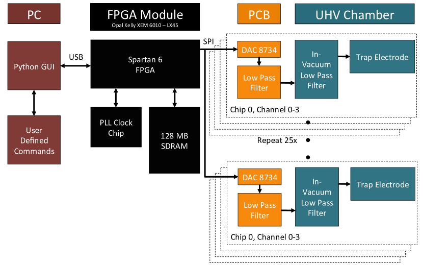
In an effort to create a low-cost scalable voltage solution, we designed a DAC system with 25 DAC8734 chips, each with 4 channels (schematic shown in Fig 11). An onboard FPGA module, the Opal Kelly XEM6010-LX45, communicates serially with each of these 25 DAC chips and enables real-time control of the voltages. This system achieves a five-fold cost reduction compared to a similar National Instruments DAC system, while also giving much better control over the update rates. Figure 11 also shows that this system can drive multiple 100-channel DAC systems, in case the overall quantum system involves multiple surface trap chips distributed over multiple vacuum chambers.
The DAC8734 chip was chosen primarily for its asynchronous nature. It has been observed that synchronous DACs whose update rates are near the ion trap frequencies cause ion heating Blakestad2009 due to peaks in the electric field noise spectrum at the update rate and its harmonics. Most commonly used two-qubit gate schemes in ion trapping systems use the ions’ shared motional state as a bus mode to generate entanglement between the ions. This requires that the motional quanta of the bus mode stays constant throughout duration of the gate, and so the heating rate will significantly impact the achievable gate fidelity. An asynchronous DAC has the advantage that updates can be paused while gates are being performed. In this way, the effect of the digital noise arising from the DACs on the fidelity of the two-qubit gates in the system can be minimized. Alternatively, synchronous DACs that update at a rate much faster than the ion trap frequencies have been found to cause little heating Bowler2012 . However, these DACs are both expensive and require significant computational overhead, as FPGA clock frequencies are typically on the same order as the update rates. Asynchronous DACs can be updated at an arbitrarily low rate, well away from the ion trap frequencies. Other than ion shuttling, our DACs are typically not updated, effectively removing the noise associated with the DAC update rate during operations that are sensitive to motional heating. Table 1 shows some of the electrical properties of the DAC8734. The 16-bit resolution enables control over the voltage down to V, and the response time is a single clock cycle (20 ns). This response time is the time the DAC takes to respond to a latch command after an update has been sent (which takes 2000 ns, or 100 clock cycles).
| DAC Resolution | 16-bits |
|---|---|
| Max Output Voltage | V |
| Max Update Rate | 430 kHz |
| Response Time | 20 ns |
| Digital Clock Frequency | MHz |
| Max Settling Time (Output changes from -10 V to 10 V) | 8 s |
For many ion trapping applications, it is important to be able to control the output of these DACs in real-time. We make use of a commercial FPGA module (Opal Kelly XEM6010-LX45). Not only does this enable forward compatibility with future FPGAs, but it also simplifies the design process, as the FPGA module includes random access memory (RAM), which enables memory-intensive operations such as ion shuttling. To control the system as a whole, we make use of multiple layers of software and hardware (shown in Figure 11). A Python program allows the user to generate a series of voltage sets to be executed. This program passes assembly code to the FPGA which is executed in real time and controls the serial outputs to the DAC chips. The voltage sets are sent from the PC to a combination of block memory on the FPGA (32 sets maximum) and RAM (8 M sets maximum) on the Opal Kelly module. When the system is not in its shuttling mode, the FPGA uploads one set of voltages to the DAC chips and then turns off all outbound clocks to reduce the noise on the DAC outputs. The FPGA interpolates between these sets at a user defined update rate ( kHz) and step size.
6.1 DAC noise analysis
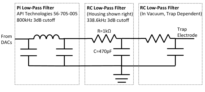
The outputs of the DACs pass through several layers of filtering before reaching the ion trap electrodes in an effort to reduce noise near the trap frequencies. These filters reduce both noise generated by the DAC system itself and noise picked up on the wires that connect the DAC system to the ion trap. It is common practice in surface electrode ion traps to use the electrodes powered by the DACs as an AC ground for the RF voltages used inside the trap. If this RF voltage has a weak ground path, it can radiate throughout the system and generate yet more noise. Within these constraints, we found it necessary to provide a good path to ground for the system at the filters immediately outside of the electrical vacuum feedthrough. The RC filters are housed in a Faraday cage machined out of a block of steel that is connected directly to both the trap ground and to a grounding strap in an effort to reduce the noise on the DAC outputs. The filters used have pF and k, with a cut off frequency kHz. This connector provides a low-resistance path to ground and acts to shield the lines after the filters from any additional noise. Commercial in-line filters (API Technologies 56-705-005 filters) with a cutoff frequency of 800 kHz were added to increase the filtering at high frequency and avoid any unwanted pickup near the self-resonant frequency of the capacitors used in the RC filters. Figure 12 shows a circuit diagram of these filters.
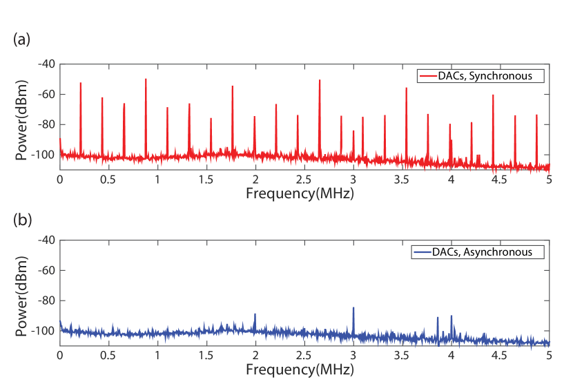
It is useful to evaluate the noise performance of the DAC system in two modes: synchronous mode, where the output voltages are updated at their maximum rate, and asynchronous mode, where the output voltages are updated once and left constant. In practice, the update rate can be anywhere between these two extremes, but synchronous mode is a good approximation of the behavior of the system during ion shuttling, and asynchronous mode is a good approximation for all other times. Figure 13 shows the noise spectrum of the output of the DAC system for both of these modes. The noise spectrum for the synchronous case clearly shows noise at the update rate (430 kHz), its half-harmonic, and its harmonics. However, much of this noise will be significantly reduced by the filters shown in figure 12.
We have demonstrated the performance of a low noise DAC system, with lower cost compared to commercially available DACs. These DACs are optimized for the common case of static ions while retaining significant shuttling capabilities. During shuttling their performance will be slower than the DACs shown by Bowler et. al. Bowler2012 , yet comparable to the NI PXI-6733 used by Shu et. al. Shu2014 . Our DAC system is significantly less expensive, easier to program, and require less computational overhead than the other two alternatives.
7 Summary and conclusion
As we scale up trapped ion quantum computing to a system large enough to perform significant quantum computations, the amount of classical hardware required will also grow. Here we described our efforts towards designing control hardware that is scalable and extensible while minimizing expense and spatial requirements. To this end, we have developed an offset frequency lock for CW lasers, such as those used for Doppler cooling, which allows many slave lasers to be locked to a single master laser, where each slave laser can also serve as a new master laser in a tree like structure. A single laser locked to a stable reference is sufficient to frequency stabilize a large number of slave lasers with little expense and space required for each slave laser lock. For pulsed laser used to drive Raman transitions, we have developed a pulsed laser Raman beam stabilization system that does not require access to the laser cavity, and can be implemented using simple and inexpensive low frequency components. With this lock the coherence time measured using a ion is 811 (69) ms, which is sufficient a large scale computation containing thousands of logic gates. Currently we are developing a general purpose PI loop system that could easily replace the pulsed laser Raman laser stabilization, intensity, and offset frequency locking controllers and software. The compact and economical system will be able to support 8 simultaneous locks with DC output, or optional off-chip DDS output. As each logic unit in the MUSIQC architecture will likely require an individual surface electrode ion trap with 100 or more DC electrodes, we have developed a low-noise, asynchronous, DAC system that compares favorably to the available commercial systems in cost, size, and flexibility.
Acknowledgements.
This work was supported by the Office of the Director of National Intelligence and Intelligence Advanced Research Projects Activity through the Army Research Office.References
- (1) D.J. Wineland, C. Monroe, W.M. Itano, D. Leibfried, B.E. King, D.M. Meekhof, Journal of Research of the National Institute of Standards and Technology 103(3), 259 (1998)
- (2) R. Blatt, D. Wineland, Nature 453(7198), 1008 (2008)
- (3) C. Langer, R. Ozeri, J.D. Jost, J. Chiaverini, B. DeMarco, A. Ben-Kish, R.B. Blakestad, J. Britton, D.B. Hume, W.M. Itano, D. Leibfried, R. Reichle, T. Rosenband, T. Schaetz, P.O. Schmidt, D.J. Wineland, Physical Review Letters 95(6), 4 (2005)
- (4) A. Myerson, D. Szwer, S. Webster, D. Allcock, M. Curtis, G. Imreh, J. Sherman, D. Stacey, A. Steane, D. Lucas, Phys. Rev. Lett. 100, 200502 (2008)
- (5) R. Noek, G. Vrijsen, D. Gaultney, E. Mount, T. Kim, P. Maunz, J. Kim, Optics letters 38(22), 4735 (2013)
- (6) J. Benhelm, G. Kirchmair, C.F. Roos, R. Blatt, Nature Physics 4(6), 463 (2008)
- (7) K. Brown, A. Wilson, Y. Colombe, C. Ospelkaus, A. Meier, E. Knill, D. Leibfried, D. Wineland, Phys. Rev. A 84, 030303 (2011)
- (8) C. Ballance, T. Harty, N. Linke, D. Lucas, arXiv preprint arXiv:1406.5473 (2014)
- (9) J.T. Merrill, C. Volin, D. Landgren, J.M. Amini, K. Wright, S.C. Doret, C.S. Pai, H. Hayden, T. Killian, D. Faircloth, K.R. Brown, A.W. Harter, R.E. Slusher, New Journal of Physics 13, 15 (2011)
- (10) D.L. Moehring, C. Highstrete, D. Stick, K.M. Fortier, R. Haltli, C. Tigges, M.G. Blain, New Journal of Physics 13 (2011)
- (11) C. Monroe, J. Kim, Science 339(6124), 1164 (2013)
- (12) C. Monroe, R. Raussendorf, A. Ruthven, K. Brown, P. Maunz, L.M. Duan, J. Kim, Physical Review A 89(2), 022317 (2014)
- (13) M.W. Lee, M.C. Jarratt, C. Marciniak, M.J. Biercuk, Optics express 22(6), 7210 (2014)
- (14) R. Drever, J. Hall, F. Kowalski, J. Hough, G. Ford, A. Munley, H. Ward, Applied Physics B 31(2), 97 (1983)
- (15) D. Hayes, D.N. Matsukevich, P. Maunz, D. Hucul, Q. Quraishi, S. Olmschenk, W. Campbell, J. Mizrahi, C. Senko, C. Monroe, Physical Review Letters 104(14) (2010)
- (16) R. Islam, W. Campbell, T. Choi, S. Clark, C. Conover, S. Debnath, E. Edwards, B. Fields, D. Hayes, D. Hucul, et al., Optics letters 39(11), 3238 (2014)
- (17) E. Mount, S.Y. Baek, M. Blain, D. Stick, D. Gaultney, S. Crain, R. Noek, T. Kim, P. Maunz, J. Kim, New Journal of Physics 15(9), 093018 (2013)
- (18) D.L. Hayes, Remote and local entanglement of ions with photons and phonons. Ph.D. thesis, University of Maryland Department of Physics and National Institute of Standards and Technology (2012)
- (19) Q.A. Turchette, D. Kielpinski, B.E. King, D. Leibfried, D.M. Meekhof, C.J. Myatt, M.A. Rowe, C.A. Sackett, C.S. Wood, W.M. Itano, C. Monroe, D.J. Wineland, Physical Review A 61(6), 8 (2000)
- (20) P. Maunz, D.L. Moehring, S. Olmschenk, K.C. Younge, D.N. Matsukevich, C. Monroe, Nature Physics 3(8), 538 (2007)
- (21) R. Blakestad, C. Ospelkaus, A. VanDevender, J. Amini, J. Britton, D. Leibfried, D. Wineland, Physical review letters 102(15), 153002 (2009)
- (22) R. Bowler, J. Gaebler, Y. Lin, T. Tan, D. Hanneke, J. Jost, J. Home, D. Leibfried, D. Wineland, Physical review letters 109(8), 080502 (2012)
- (23) G. Shu, G. Vittorini, A. Buikema, C. Nichols, C. Volin, D. Stick, K.R. Brown, Physical Review A 89(6), 062308 (2014)
- (24) National Instruments PXI-6733. Datasheet (2009)