Electron localization and optical absorption of polygonal quantum rings
Abstract
We investigate theoretically polygonal quantum rings and focus mostly on the triangular geometry where the corner effects are maximal. Such rings can be seen as short core-shell nanowires, a generation of semiconductor heterostructures with multiple applications. We show how the geometry of the sample determines the electronic energy spectrum, and also the localization of electrons, with effects on the optical absorption. In particular, we show that irrespective of the ring shape low-energy electrons are always attracted by corners and are localized in their vicinity. The absorption spectrum in the presence of a magnetic field shows only two peaks within the corner-localized state domain, each associated with different circular polarization. This picture may be changed by an external electric field which allows previously forbidden transitions, and thus enables the number of corners to be determined. We show that polygonal quantum rings allow absorption of waves from distant ranges of the electromagnetic spectrum within one sample.
pacs:
73.21.La, 73.22.Dj, 78.67.HcI Introduction
Recently it has become feasible to grow core-multiple-shell nanowires consisting of a core built of one type of material which is surrounded by one or more shells of different materials. This preparation method makes achievable a huge variety of heterostructures with various and controllable properties which make them extremely attractive as building blocks of nanoelectronic and optoelectronic nanodevices, in particular solar cells Krogstrup et al. (20); Peköz et al. (2011); Tang et al. (2011); Wang et al. (2014) or nanoantennas Kim et al. (2015). In particular, nanowires of triangular cross section turned out to be a very good host for robust and efficient coaxial p-i-n junctions Dong et al. (2009) or multicolor nanophotonic sources with controllable wavelengths Gradečak et al. (2005); Qian et al. (2004, 2005, 2008). Besides these applications, we would also like to mention a basic theoretical interest in polygonal rings as particular examples of quantum graphs Berkolaiko and Kuchment (2012) with characteristic physical behaviors. Such nanowires are usually grown vertically and, due to the crystallographic structure, have polygonal cross sections, most commonly hexagonal Blömers et al. (2013); Rieger et al. (2012); Haas et al. (2013), but triangular Qian et al. (2004, 2005); Baird et al. (2009); Dong et al. (2009), square Fan et al. (2006); Shtrikman et al. (2009), and dodecagonal Rieger et al. (2015) cross sections are also feasible. Sharp edges along the wires induce unique carrier localization, which leads to formation of one-dimensional (1D) channels in corner or side areas Jadczak et al. (2014); Bertoni et al. (2011); Royo et al. (2013, 2014, 2015); Fickenscher et al. (2013); Shi et al. .
Core-shell structures allow for modeling of many properties including band alignment which strongly depends on the strain in the system and may be controlled through the core and/or shell thickness Pistol and Pryor (2008). In such a way one may grow systems in which electrons are confined only in the shell area Blömers et al. (2013). It is also possible to etch the core part and achieve hollow nanowires Rieger et al. (2012); Haas et al. (2013), i.e., nanotubes of finite thickness. Multishell structures allow growth of narrow (up to nm) tubes which are formed between two shell layers such that surface effects are reduced Jadczak et al. (2014); Fickenscher et al. (2013); Shi et al. . A polygonal nanoring may be considered as a short wire of this kind.
Some insight has already been gained for hexagonal quantum rings which due to their symmetry and the possibility to localize electrons in the corners are refereed to as artificial benzene Ballester et al. (2012). Electron localization at the corners of a polygonal quantum ring is expected if one notes that localization occurs whenever a nanowire is bent. Indeed, electronic states on nanowire bends, which in our case are the corners of the polygonal contour, attracted much interest some years ago Lent (1990); Sols and Macucci (1990); Sprung et al. (1992); Wu et al. (1992a, b); Wu and Sprung (1993); Vacek et al. (1993); Xu (1993). In a single-mode wire with a circular bend a simplified 1D picture was obtained in which the corner may be replaced by a square well, whose depth and length are determined by the angle and radius of the circular bend Sprung et al. (1992). This approach was used in Ref. Estarellas and Serra (2015) to suggest a scattering model of 1D polygonal wires, treating each corner as a scatterer. However, in contrast to our present purpose, the authors of Ref. Estarellas and Serra (2015) considered only the extended states along the sides of the 1D polygon. In fact, contrary to hexagonal quantum dot molecules, rings also allow localization of charge carriers in side areas, and they can even favor one of the sides if that is sufficiently thick Ballester et al. (2012). Other related effects, like the suppression of the Aharonov-Bohm effect in hexagonal rings, have also been theoretically envisioned Ballester et al. (2013).
In this paper we study electron localization in polygonal quantum rings of various shapes and show how it determines optical absorption. We use a computational method based on finite differences on a polar grid which enables us to model not only hexagonal structures but arbitrary polygonal rings including nonsymmetric samples. We also derive the localized states with a 1D scattering model. We focus mostly on triangular rings, where the corner-to-edge ratio is largest, resulting in the most pronounced localization and corresponding optical effects. We show that irrespective of sample shape one can always distinguish a group of corner-localized states which for some geometries are separated by an energy gap from the higher states. The electron localization pattern is very sensitive to sample symmetry and shape. For quantum rings defined by regular polygonal constraints the localization probability is equally distributed between all corners and/or sides of the ring, but when the symmetry is broken, e.g., by different side thicknesses or corner softening, the probability density becomes localized on individual corners which are occupied according to their areas. External electric fields may partially control electron localization, by destroying equal distribution between corners, or by delocalizing states previously occupying a single corner area.
We analyze optical absorption of the systems and show that in the presence of a perpendicular magnetic field only two transitions occur from the ground-state to corner- and side-localized domains, each associated with different polarization. Still, external electric fields may break the wave function symmetry such that more transitions become visible, and thus optical experiments may allow to infer the number of corners. Moreover, we point out that triangular quantum rings allow absorption in the microwave and near-infrared regimes to be observed within the same sample.
The paper is organized as follows. In Sec. II we define the analyzed systems and make a preliminary inspection of the low-energy states in polygonal rings based on the 1D scattering model. Then, in Sec. III we introduce the sample model and describe the discretization method. In Sec. IV we present the low-energy quantum states resulting from our Hamiltonian model. Then in Sec. V we calculate optical spectra corresponding to excitation of electrons initially in the ground-state. Finally, Sec. VI contains conclusions and final remarks.
II The 1D scattering model
The systems under study are two-dimensional (2D) polygonal quantum rings of different shapes. They may also be considered as short core-multiple-shell or hollow nanowires such that all electronic wave functions include only the lowest axial mode. The first part of our analysis is based on a 1D scattering model. A circular bend in a nanowire with a single transverse mode acts approximately like a 1D square-well potential of depth and length Sprung et al. (1992). The bend radius and angle determine the effective square-well potential through the expressions and . Such a potential always supports bound states that, physically, represent states localized on the wire bend Lent (1990); Sols and Macucci (1990); Sprung et al. (1992); Wu et al. (1992a, b); Wu and Sprung (1993); Vacek et al. (1993); Xu (1993). This type of effective confinement is the physical mechanism behind the corner localization that occurs in polygonal nanorings of finite width, which will be discussed in detail in Sec. IV.
It is possible to devise a 1D model, whose only coordinate is the position along the nanoring perimeter, say , with cyclic boundary conditions on the wave function ; namely , where is the full perimeter length. Each corner acts like a point scatterer, characterized by a scattering matrix given by a square well. Using this 1D model the authors of Ref. Estarellas and Serra (2015) described the states propagating along the polygon sides. Here we extend that analysis to negative-energy states, localized on the corners and behaving as evanescent waves on the polygon sides.
The wave function between vertices and is a combination of right () and left () propagating plane waves,
| (1) | |||||
where label the vertices, are their positions, and the wave number is purely imaginary. For a total energy lower than the first transverse mode of the wire it is . The scattering amplitudes in Eq. (1) fulfill a linear homogeneous system given by the scattering relation
| (2) |
and the condition between successive vertices
| (3) | |||||
| (4) |
In Eq. (2) and are the reflection and transmission scattering amplitudes of the above mentioned squared well for imaginary wave numbers. The energies for which Eqs. (2), (3), and (4) admit a solution can be determined from the zeros of the determinant of the linear system matrix , or equivalently, of the function Estarellas and Serra (2015)
| (5) |
where is analogous to except for an arbitrarily chosen scattering amplitude which is set to 1.
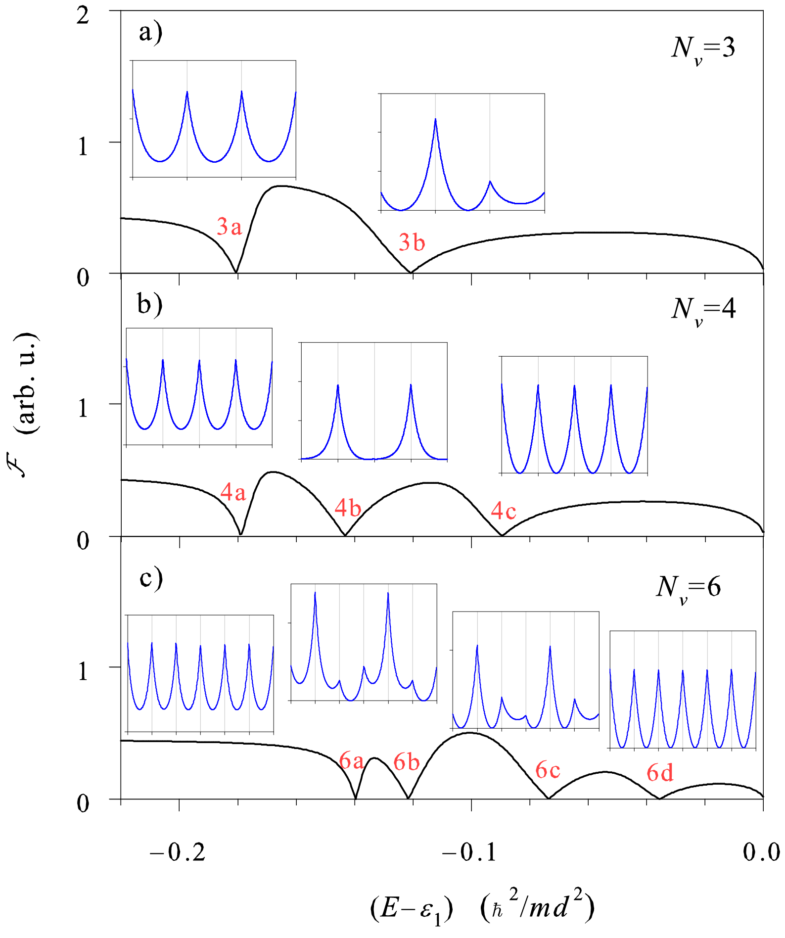
Figure 1 shows the energy dependence of for a triangular, a square, and a hexagonal sample. The sequence of allowed energies in each polygonal nanoring is seen from the zeros while the figure insets show the corresponding 1D densities for each mode (labeled as a, b, etc.). The probability densities are concentrated on the corners and the modes can be classified into two types: translational symmetric modes (TSM’s) having the same density on each segment of the polygon and translational asymmetric modes (TAM’s) for which the sides look different. The TAM’s (3b, 4b, 6b, 6c) are degenerate, since inversion from the central point leads to another valid solution. Counting also the spin, the degeneracy factors become 2 for symmetric modes and 4 for asymmetric ones.
A closer look at the TSM’s of Fig. 1 reveals that there are two types, depending on the density at each side midpoint. Modes 3a, 4a, and 6a have finite midpoint densities while modes 4c and 6d exactly vanish at midpoints. With a similar analysis as that of Ref. Estarellas and Serra (2015) it can be shown that the first type (3a, 4a, 6a) occurs when . The second type of TSM’s (4c, 6d) correspond to the condition and occur only in even polygons. We also notice that the energies of the TAM’s lie in between the TSM’s. The sequence is such that in odd- polygons there are TAM’s between TSM’s, while in even- polygons there are intermediate TAM’s. In all cases, however, this sequence of localized states abruptly terminates at the side-propagating threshold .
III The Hamiltonian model
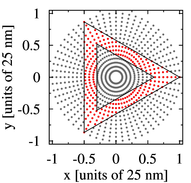
The second part of our modeling is based on a discretization method on a polar grid. We start with a circular disk geometry as in Ref. Daday et al., 2011 on which we apply polygonal constraints and pick up only points within the resulting shell (Fig. 2). In this case the Hilbert space is spanned by vectors , where and label the discretized radial and angular coordinates , with meshes (), respectively, and stands for the two possible spin values.
The system Hamiltonian consists of four terms,
| (6) |
Hamiltonian matrix elements of the first contribution, the kinetic Hamiltonian, in the , , and basis are
| (7) |
where is a reference energy, is the effective mass of the semiconductor material, is the external radius of the polar grid, , and .
We expose the rings to external electric and magnetic fields. The electric field is parallel to the - plane and forms an angle with the axis, , and the corresponding Hamiltonian matrix elements are
where is the electron charge. The magnetic field is assumed perpendicular to the ring plane, with a vector potential , and the corresponding Hamiltonian matrix elements are obtained as
with the cyclotron energy in units of .
The last contribution to the Hamiltonian, the Zeeman part, is diagonal in the and basis
| (8) |
where is the ratio between the Zeeman gap and the cyclotron energy, and is the free-electron mass. Our discretization method is a version of the very popular hopping schemes used in the mesoscopic physics. Other theoretical studies of core-shell polygonal systems used the finite-element method Fickenscher et al. (2013); Wong et al. (2011); Royo et al. (2015).
IV Electronic states
Below we present results for 2D polygonal rings achieved with the discretization method where the sample consists of over 6000 grid points. We use the external radius nm. We perform numerical calculations for InAs parameters which are , where is the electron mass, and ; thus the energy unit introduced in the Hamiltonian (III) equals approximately meV and the ratio .
IV.1 Symmetric samples
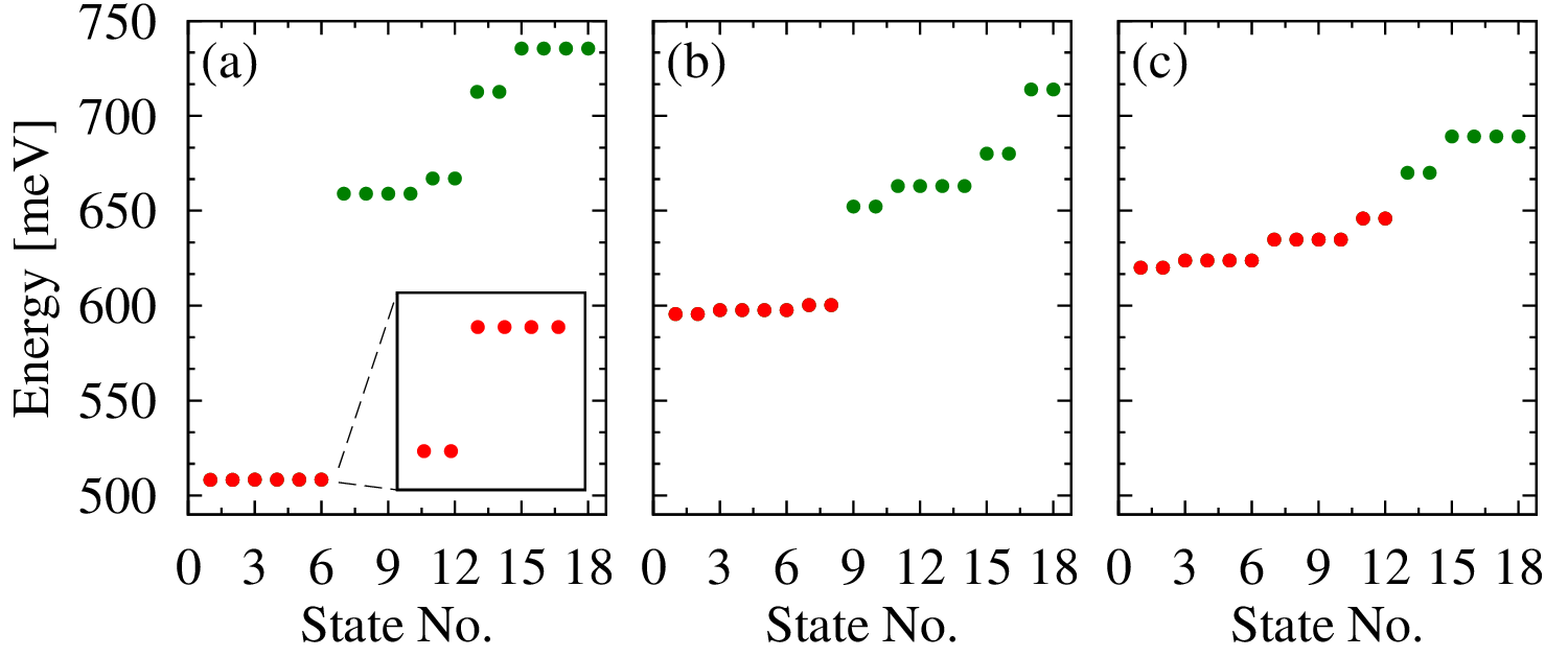
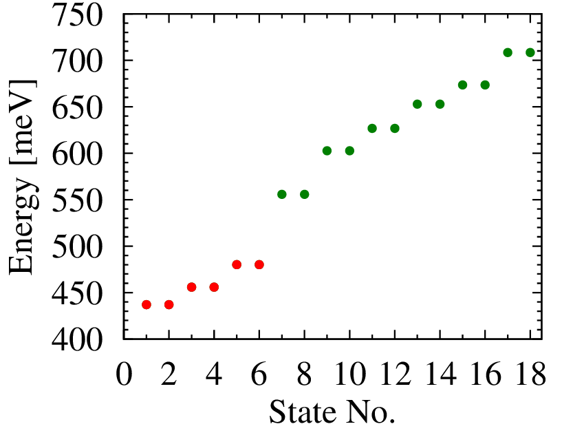
Symmetric polygonal samples which are restricted externally and internally by regular polygons have well defined symmetries which imply specific energy degeneracies. In Fig. 3 we compare the energy levels of a single electron confined in symmetric triangular, square, and hexagonal rings, all having sharp corners and nm side thicknesses, in the absence of external fields. As can be seen, the ground-state energy increases with the number of corners. This is because the size of the effective well formed in the corner area decreases with increasing corner angle, and thus ground-state electrons bounded in corners of the regular hexagon have higher energy than those trapped in corners of regular triangles. This is in a nice qualitative agreement with the results shown in Fig. 1. In a circular nanoring the ground-state has zero angular momentum and it is doubly (spin) degenerate, whereas all higher states are fourfold degenerate, having finite angular momenta that do not distinguish energetically between clockwise and counterclockwise electron rotations Fuhrer et al. (2001); Aichinger et al. (2006); Niţă et al. (2011). When the regular polygonal constraints are applied to a ring structure they break the circular degeneracy at levels corresponding to multiples of . The resulting series of two- and fourfold degenerate energy levels agree with the expectation from Sec. II where spin was ignored.
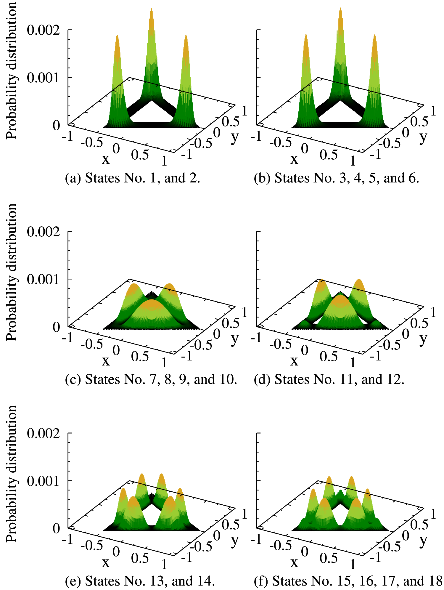
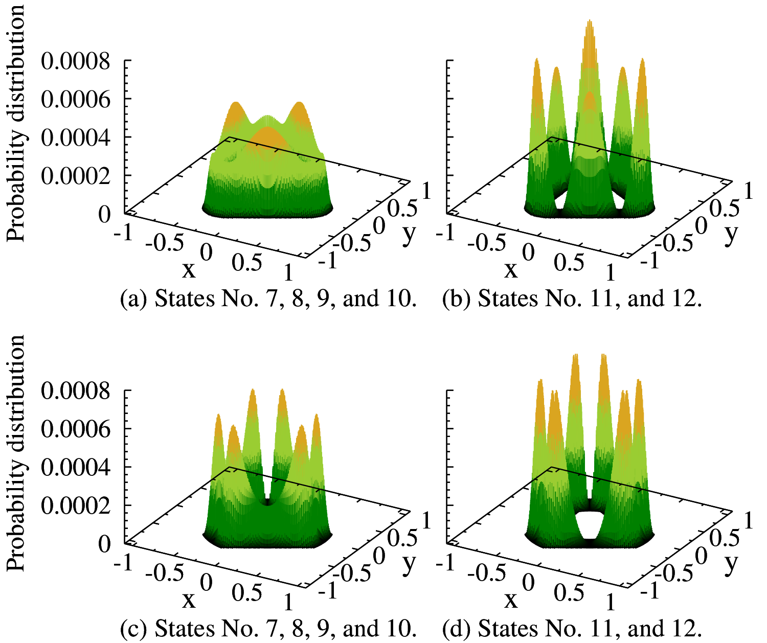
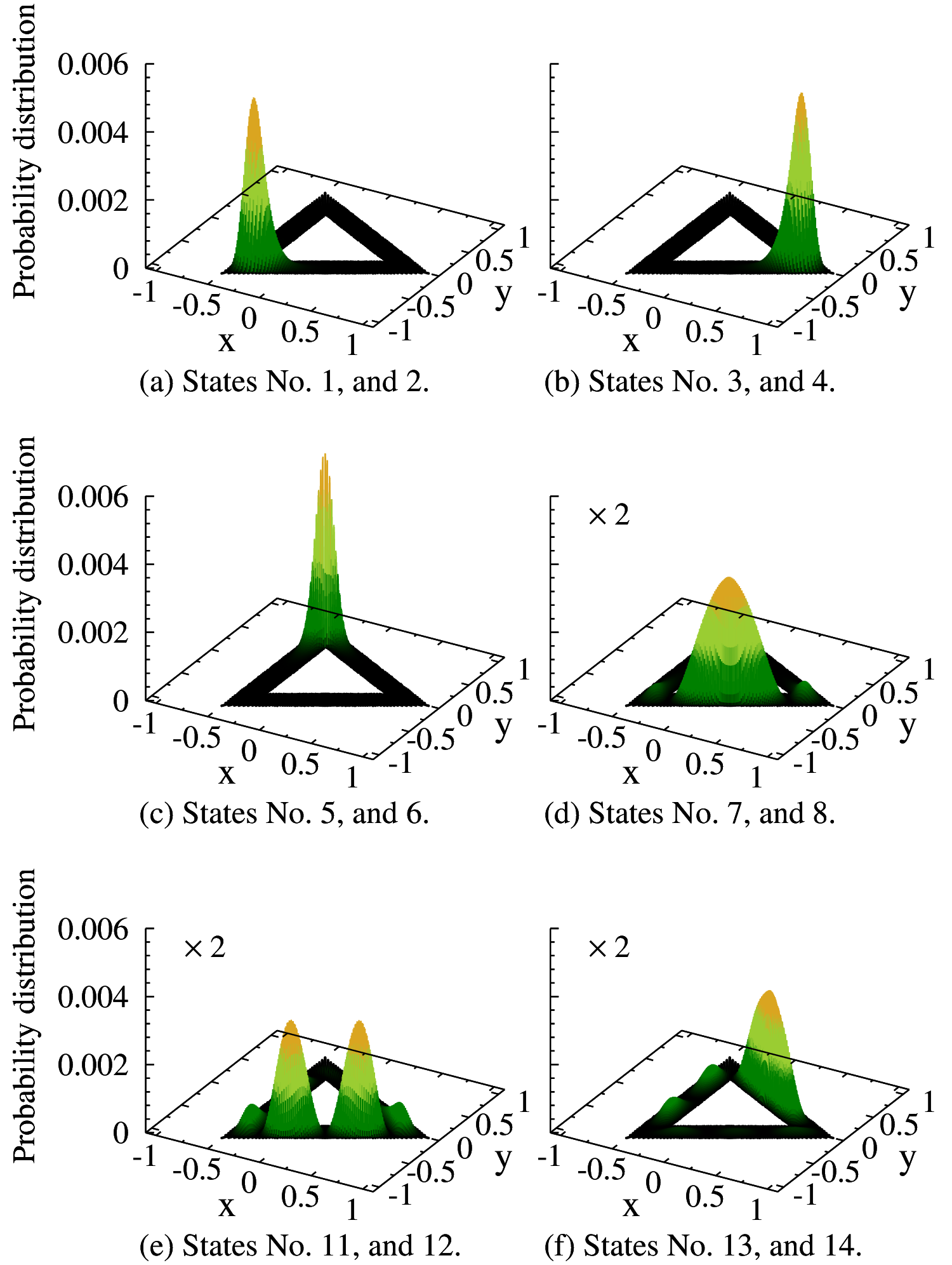
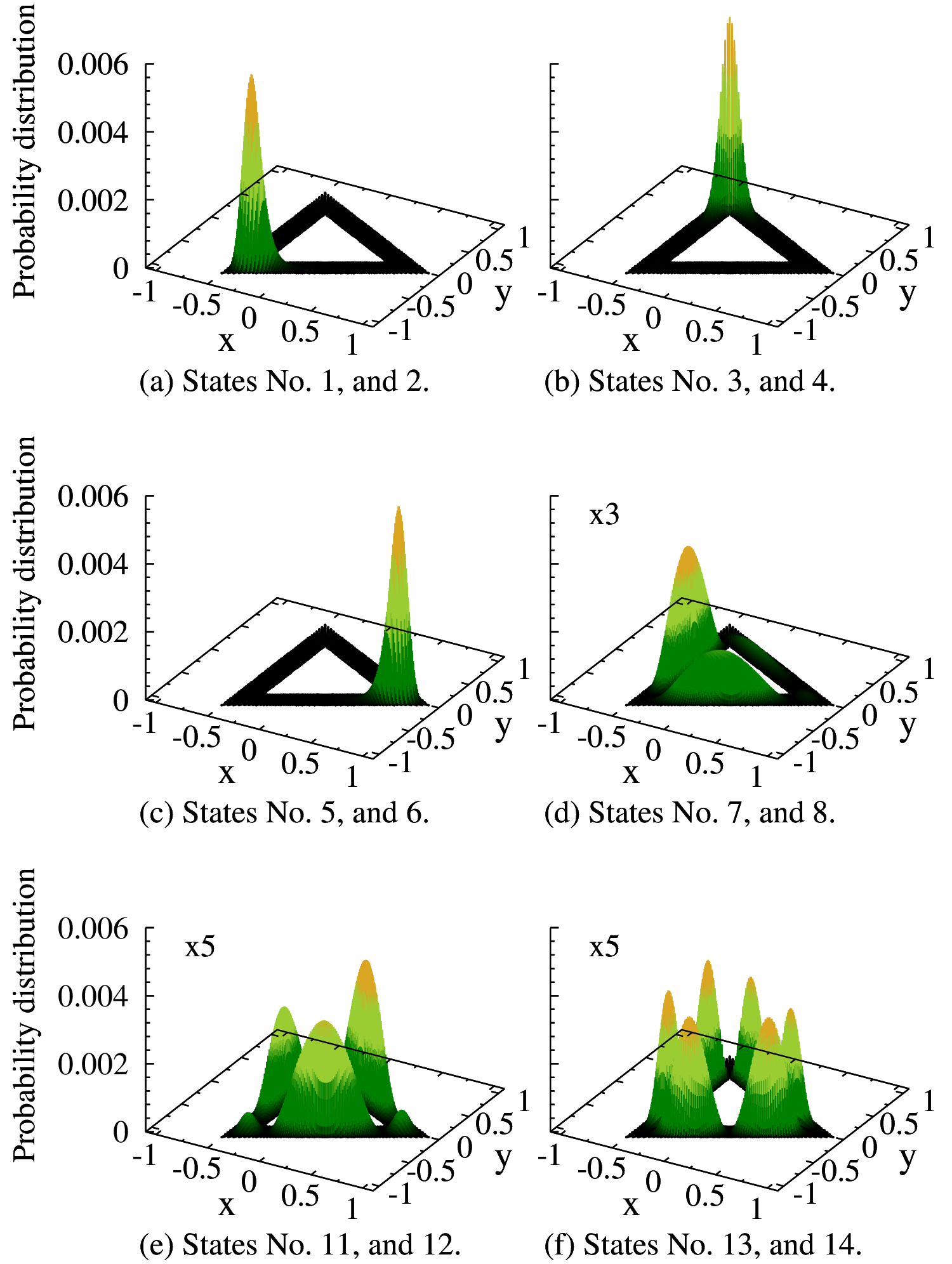
In Fig. 3(a) a group of the six lowest states of the triangular ring is separated from the higher states. The energy gap behind the eighth state is still visible for a square polygon [Fig. 3(b)], but considerably decreased with respect to the triangular sample, and it practically vanishes for a hexagonal ring [Fig. 3(c)]. Although the energy spacing between the th and th states of the artificial benzene is comparable with other energy differences, in this case also the lowest states have different character from the others. States associated with the lowest energy levels of symmetric polygonal rings (red points in Fig. 3) are equally distributed between all of the corners, as is shown for a triangular ring in Figs. 4(a), and 4(b). Due to the spin degeneracy the number of these states equals double the number of corners (). If the sample is thick enough and contains a sufficient number of corners the probability distribution does not vanish completely in the middle of the sides, as for the triangular ring shown in Fig. 4, but stabilizes at a much lower level than the corner maxima. The first state above the corner states is purely localized in sides, with maximal probability of finding a particle in the middle of each side [Fig. 4(c)]; higher energy electrons are also mostly localized in the side areas with only a small probability of finding them in corners [Fig. 4(d)]. The number of probability maxima in the side regions increases with energy and the possibility of finding them in corners becomes relevant [Figs. 4(e), and 4(f)]. The probability of finding electrons in sharp corners becomes comparable to or even exceeds side maxima for high-energy electrons, but the detailed analysis of such states is beyond the scope of this paper.
For the lowest, corner-localized states, the probability density maxima decrease with increasing number of corners and at the same time the density of localization areas increases, similarly, for the first state above them the number of maxima increases and the distances between them decrease with an increasing number of corners, i.e., the side localization areas decrease. As a result the probability distributions for corner- and side-localized states become relatively similar and thus the energy gap occurring for triangular and square quantum rings [Figs. 3(a) and 3(b)] vanishes for sufficiently thick hexagonal samples [Fig. 3(c)]. However, the corner-localized states of artificial benzene may also be energetically separated from the higher states when the rings are very narrow such that the corner-localization areas are much smaller than the side ones.
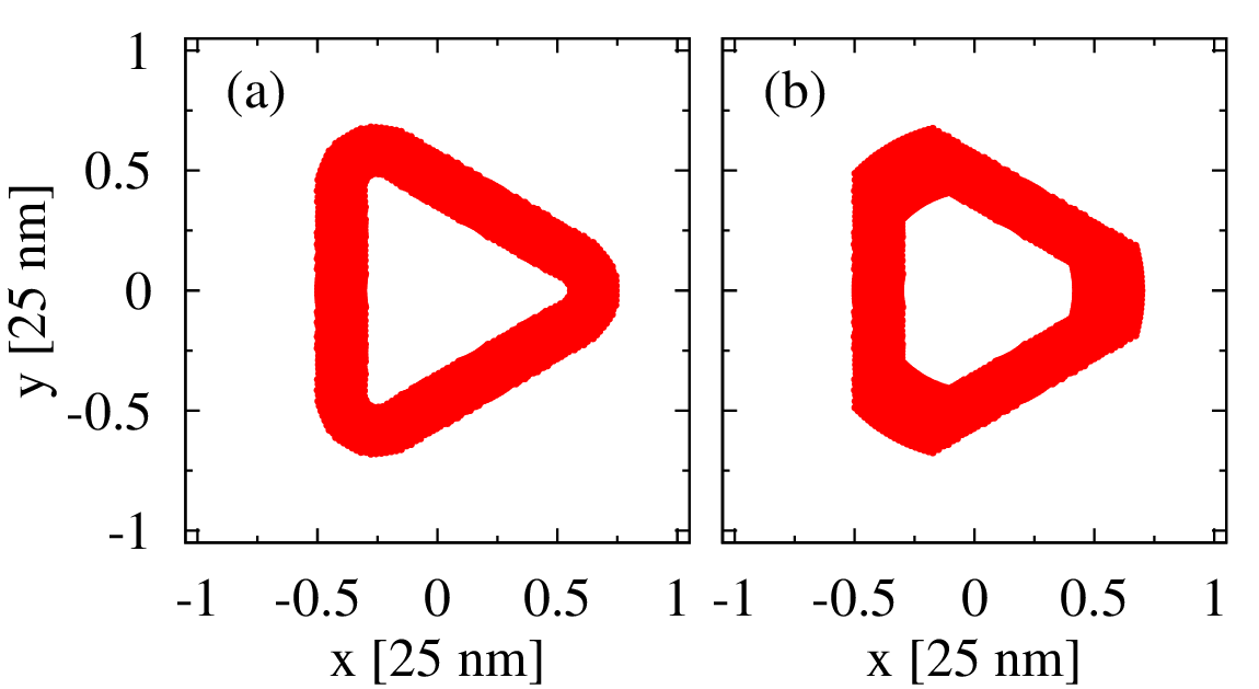
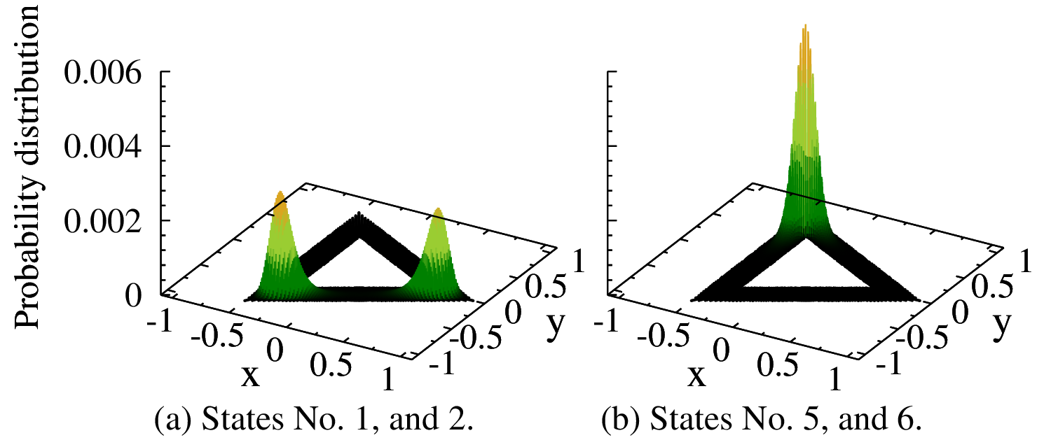
In practice it may be difficult to achieve samples with perfectly sharp corners. Therefore we investigated the impact of corner softening on energy levels and carrier localizations. We analyze two types of symmetric triangular samples shown in Fig. 5, in one case we inscribe circles in the corners which define new internal and external limits in corner areas [Fig. 5(a)]; in the other case we soften corners by ´cutting´ the sharp parts by background radii [Fig. 5(b)]. In both cases energy levels show the same degeneracies as for the samples with sharp corners [Fig. 3(a)]. Moreover, the lowest six states associated with the two lowest energy levels are always localized in corner areas. If all of the corners are equally softened and when the softening is relatively small, which for -nm-thick samples means that the radii reduction for the sample shown in Fig. 5(b) must be up to around , then the probability density for samples with soft corners does not differ considerably from the one shown in Fig. 4. There are many possibilities of softening internal and external corners separately; thus there is a huge variety of samples which show properties of ideal (sharp) ones. Interesting features appear when these limits are exceeded. In the case of the sample shown in Fig. 5(a) the energy gap separating the purely corner-localized states is comparable with energy splittings occurring in the next higher states. Those states can be distributed both in the corners and on the sides [Figs. 6(a) and 6(b)].
The energy separating the two lowest energy levels exists in samples with ´cut´ corners, like the one shown in Fig. 5(b), but it decreases due to softening. In contrast to the samples with sharp corners, where the lowest six states are localized in the corners and the next six (th to th) states are localized on the sides of the triangle (Fig. 4), now the states associated with the two levels above the energy gap (th to th states) are still localized in the corner area, but each one has two nearby maxima. In fact corner softening of this kind increases the number of corners, and the sample may show mixed features of triangles and hexagons. Three corner maxima split in each corner area such that six maxima are formed [Figs. 6(c) and 6(d)] and the transition to mostly (not purely) side-localized states occurs above the fourth energy level as for hexagonal samples.
IV.2 Nonsymmetric samples
Although the present state of the art of manufacturing allows high precision control at the single-atom level, it is still difficult to grow perfectly symmetric nanowires, and thus we also analyze different nonsymmetric samples. First we break the symmetry by increasing the thickness of two sides by and . In this case the energy levels are only spin degenerate and the energy gap between the sixth and seventh states is reduced with respect to the symmetric case, but it is still relevant (Fig. 7). The lowest states are also localized in corner areas (red points in Fig. 7), but the probability distribution is not spread on all corners as before: electrons of specific energy values occupy only one corner. In particular, the ground-state is localized in the corner with the largest area [Fig. 8(a)], the two states associated with the second energy level occupy the corner with the medium area [Fig. 8(b)], and the electrons possessing the third energy value may be found in the smallest corner, Fig. 8(c). The first state above the corner localized group is mostly localized in the side region with small probability peaks in corners [Fig. 8(d)]. In general the number of probability peaks increases with the energy. But unlike what happens in a symmetric polygon, one can obtain states with probability distribution concentrated in fewer places than in lower-energy states, as is shown in Figs. 8(e) and 8(f). Similar situations (not shown) occur for rings which are defined by nonsymmetric polygons with uniform thicknesses, but nonuniform angles. Since the wells formed in corner areas of polygonal rings depend on the angle geometry, they become nonsymmetric when the polygonal sides have different thicknesses. Thus when one side of the polygon is thicker than the others then the wells formed at its ends have the largest areas and are shifted towards the center of the thicker side. This results in delocalization for the ground-state electrons in those corner areas and shifting them towards the center of the widest side with increasing side thickness. For sufficiently thick sides the wells merge, and the ground-state becomes localized in the middle of the thicker side, as shown in Ref. Ballester et al., 2012.
The electron probability density may be controlled externally by applying electric fields. On one hand this may break the symmetric distribution of regular samples; on the other hand it may rebuild, if not perfectly then to some extent, a symmetric distribution in nonsymmetric samples. In Fig. 9 we show electron localization for a geometrically symmetric sample in the presence of an external electric field parallel to one of the sides (forming an angle with the axis). The electron localization resembles much more that of the nonsymmetric triangle (Fig. 8) than that of the regular one (Fig. 4). But, in contrast to the case with different side thicknesses, here one can change the order of corner occupation. For example, with the electric field rotated such that it becomes parallel to the axis, the ground-state would be localized as in Fig. 9(a), but the corner areas associated with the two higher energy levels would be reversed with respect to Fig. 9. Or the field perpendicular to one side may localize the ground-state in the opposite corner, whereas the two higher (nearly degenerate) energy levels become equally distributed between the remaining two corners.
If the previously described sample with different side thicknesses is placed in an external electric field, then it is quite easy to delocalize the ground and the first excited states between the corners at the ends of the widest side [Fig. 10(a)] while the probability distribution of the highest corner-localized state remains localized in the smallest corner [Fig. 10(b)]. Restoration of equal distribution between all three corners is impossible due to the particular shapes and areas of the quantum wells formed in the corners, which strongly differ from each other and cannot be compensated by an external electric field for any angle .
V Optical absorption
We describe the interaction of electrons in the polygonal rings with an external radiation field in the dipole approximation. The optical absorption coefficient at zero temperature is given by the well-known formula Haug and Koch (2009); Chuang (1995); Hu et al. (2000)
| (9) |
with being a constant containing physical parameters such as the refractive index, the speed of light, the dielectric permittivity, and the sample area, the circular photon polarization, the dipole moment, and the energies of the initial and final states , respectively. The dipole matrix elements are
where the summation is carried out over all possible basis states and are the amplitudes of the eigenvectors of Hamiltonian (6) in the basis, , where . We approximate the function by the spectral weight in the presence of a constant self-energy ,
| (10) |
corresponding to a phenomenological broadening of the discrete spectrum of the polygonal ring.
The localization properties discussed in Sec. IV govern the optical absorption through the dipole matrix elements , which depend on the shapes of the wave functions corresponding to states and . For simplicity we consider a weak ( T) magnetic field perpendicular to the ring plane which lifts both degeneracies (due to spin and rotation), but does not considerably affect the electron localization. The chosen magnetic field produces a Zeeman splitting of 0.48 meV. Since we do not include a spin-orbit interaction optical transitions may occur only between states with the same spin. We restrict the investigation to two groups of states, corner-localized states and the group consisting of the same number of states above them. For symmetric samples with sharp corners the latter states are purely or mostly side-localized [Figs. 4(c) and 4(d) for a triangular sample]. We assume that the system is initially in the ground state, that is, one electron occupies the lowest energy level and we assume a broadening parameter meV.
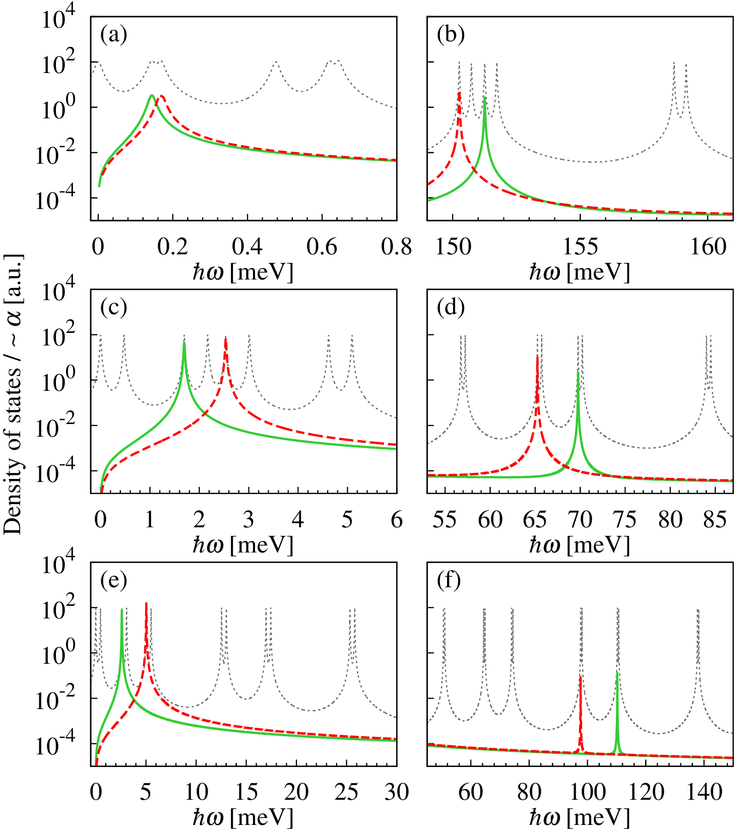
In Fig. 11 we compare the absorption spectrum of symmetric triangular [Figs. 11(a) and 11(b)], square [Figs. 11(c) and 11(d)], and hexagonal [Figs. 11(e) and 11(f)] samples with sharp corners. We plot all energy intervals between the ground-state and the corner- [(a), (c), and (e)] or side-localized [(b), (d), and (f)] states, respectively, on which we superimpose the optical absorption coefficient calculated according to the formula (9) for an electromagnetic wave circularly polarized in the - plane. In principle, for a triangular ring two transitions to the corner-localized and three transitions to the states above the energy gap should be observed. As can be seen, both transitions to the lowest-state domain occur, but each one is coupled with a different orientation of the photon polarization. The reason is that the magnetic field, which points along the positive direction, creates an orbital splitting of the first two excited states. The lower of them rotates clockwise in the - plane, whereas the higher rotates counterclockwise. Although three out of the six states shown in Fig. 11(b) have the same spin as the initial state, only two optical transitions are observed to states which in the absence of a magnetic field would belong to the first, fourfold degenerate energy level above the energy gap. As in the previous case each transition is observed in the presence of only one polarization direction. The same tendency, i.e., coupling of the ground-state (twofold degenerate at zero magnetic field) to one of fourfold degenerate states (at zero magnetic field) occurs also for transitions to higher states (not shown). Also, if an electron is initially in a state from the group of fourfold degenerate states then for one polarization orientation it may be excited to the twofold degenerate states and for the other polarization to a fourfold degenerate one. Since for the analyzed triangular sample energy separations between corner-localized states are on the order of tens of meV and the energy distance from the ground-state to the side-localized states ranges from 150 to 160 meV, thus excitation of the ground-state to one of the corner-localized states requires absorption of microwave photons, while transitions to the side-localized states occur in the presence of a near-infrared field. This means that one sample may absorb electromagnetic waves with wavelengths differing by orders of magnitude.
Samples with more corners, in principle, could be expected to allow more transitions because there are more states with the same spin orientation (four for a square and six for a hexagon in each domain). But as shown in Figs. 11(c), 11(d), 11(e), and 11(f), still only two transitions in each state group occur. The absorption coefficient for transitions to corner-localized states increases with the number of corners, while the ratio between its value for transitions to side-localized states and transitions to corner-localized states rapidly decreases from over for triangular rings to values on the order of for hexagonal samples. Moreover, the magnitude of the absorption coefficient depends on the polarization type. In the absence of an external electric field it is usually higher for counterclockwise-polarized light. The splitting of the dipole-active absorption peak into mainly two peaks with a growing magnetic field is a well-known phenomena for quantum dots of various shapes Gudmundsson and Gerhardts (1991); Krahne et al. (2001); Magnúsdóttir and Gudmundsson (1999). The same can be stated about the opposite trends for the evolution of the height of the two absorption peaks with increasing magnetic field.
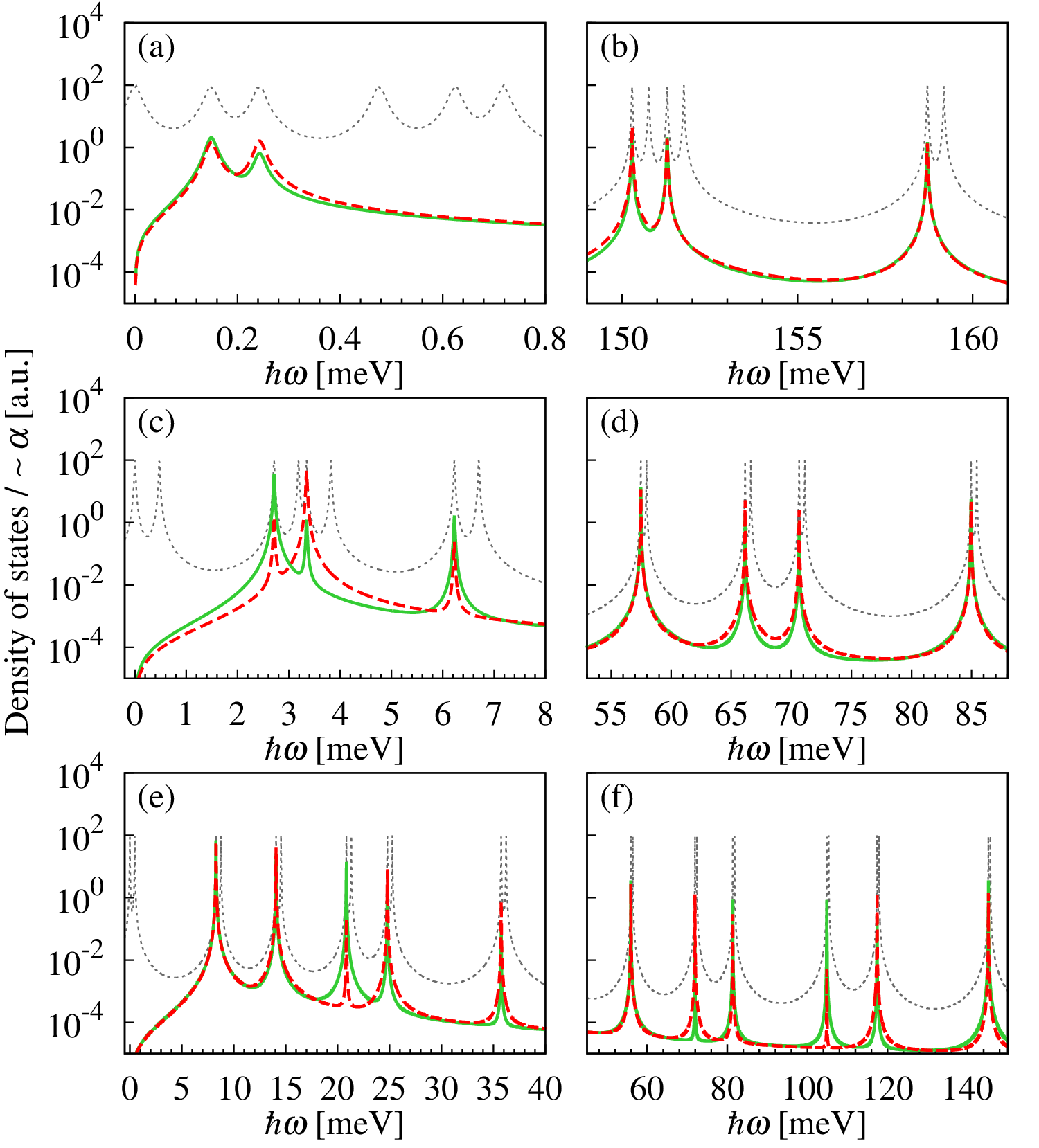
An external electric field may change the picture, as is shown in Fig. 12 where the field is applied in the ring plane. For both polarization directions all spin-allowed transitions take place, but with different values of the absorption coefficient, which shows that optical experiments may be used to probe the sample geometry. The electric field strength which allows all transitions to be ”opened” increases with the number of corners. Triangular samples require weak fields because their corners are relatively well separated, while corners of a hexagon defined by the same radius are much closer to each other and thus an electric field of the same value only slightly changes the height of the localization peaks. The dipole matrix elements depend on the symmetry of the wave function and may vanish for some pairs of states, as in the case of transition to the fifth state in Fig. 11(b). But the electric field breaks the wave function symmetry (and shifts the energy levels), and thus it also changes the matrix elements and opens some other transitions, like the one from the ground to the fifth state [Fig. 12(b)]. When the electric field is strong enough to induce localization in single corner areas, then transitions to side-localized states are much more pronounced than those to corner-localized ones. The same situation, for the same symmetry reasons, is observed for the non symmetric sample shown in Fig. 8. The absorption spectrum is also sensitive to the angle which the field forms with the axis; rotation of the field may open, close, or change the strength of some transitions.
VI Conclusions
We studied spectral and optical properties of 2D polygonal quantum rings. We showed that the polygonal geometry induces two- and fourfold degeneracies and formation of an energy gap which depends on the number of corners and the lateral side thickness. In general the lowest energy states are localized in corner areas, forming a low-energy shell. The probability density is very sensitive to the ring shape. Even if the geometry of the sample only slightly differs from a regular ring, the electron localization becomes strongly nonuniform around the polygon. The charge carriers in the ground-state are always localized in the corner with the largest area. A certain softening of the corners changes the electron localization only of higher energy-states. The localization pattern may be, to some extent, controlled by an external electric field, which may change the effective potential wells associated with corners. This may also result in breaking the symmetry of regular polygons as inducing a symmetric probability distribution in nonsymmetric samples.
In order to predict basic optical properties related to the corner localization, we calculated the absorption coefficient using the linear response method. We did not include spin-orbit interaction, and thus optical transitions occur only between states with the same spin. Other selection rules are related to the symmetry of the wave functions. Some transitions are forbidden and others are allowed depending on the (circular right or left) photon polarization. In the absence of an external electric field only two transitions from the ground-state to the next higher corner-localized states and side-localized states occur. We showed that, as in to long triangular core-multishell wires Gradečak et al. (2005); Qian et al. (2004, 2005, 2008), triangular rings interact with radiation from different domains, possibly microwave and near-infrared at the same time. Since the external electric field changes the wave function geometry, it also affects the absorption coefficient through the dipole matrix elements and “opens” previously “closed” transitions, blocks others or changes their intensity , i.e., allows contactless control of optical properties.
Acknowledgements.
This work was financially supported by the Research Fund of the University of Iceland, the Nordic network NANOCON- TROL, project No.: P-13053, and by MINECO-Spain (Grant No. FIS2011-23526).References
- Krogstrup et al. (20) P. Krogstrup, H. I. Jorgensen, M. Heiss, O. Demichel, J. V. Holm, M. Aagesen, J. Nygard, and A. Fontcuberta i Morral, Nature Photonics 7, 306–310 (2013).
- Peköz et al. (2011) R. Peköz, O. B. Malcıoğlu, and J.-Y. Raty, Phys. Rev. B 83, 035317 (2011).
- Tang et al. (2011) J. Tang, Z. Huo, S. Brittman, H. Gao, and P. Yang, Nature Nanotechnology 6, 568 (2011).
- Wang et al. (2014) K. Wang, S. C. Rai, J. Marmon, J. Chen, K. Yao, S. Wozny, B. Cao, Y. Yan, Y. Zhang, and W. Zhou, Nanoscale 6, 3679 (2014).
- Kim et al. (2015) S.-K. Kim, X. Zhang, D. J. Hill, K.-D. Song, J.-S. Park, H.-G. Park, and J. F. Cahoon, Nano Letters 15, 753 (2015), pMID: 25546325, http://dx.doi.org/10.1021/nl504462e .
- Dong et al. (2009) Y. Dong, B. Tian, T. J. Kempa, and C. M. Lieber, Nano Letters 9, 2183 (2009), pMID: 19435385, http://dx.doi.org/10.1021/nl900858v .
- Gradečak et al. (2005) S. Gradečak, F. Qian, Y. Li, H.-G. Park, and C. M. Lieber, Applied Physics Letters 87, 173111 (2005).
- Qian et al. (2004) F. Qian, Y. Li, S. Gradečak, D. Wang, C. J. Barrelet, and C. M. Lieber, Nano Letters 4, 1975 (2004), http://dx.doi.org/10.1021/nl0487774 .
- Qian et al. (2005) F. Qian, S. Gradečak, Y. Li, C.-Y. Wen, and C. M. Lieber, Nano Letters 5, 2287 (2005), pMID: 16277469, http://dx.doi.org/10.1021/nl051689e .
- Qian et al. (2008) F. Qian, Y. Li, S. Gradecak, H.-G. Park, Y. Dong, Y. Ding, Z. L. Wang, and C. M. Lieber, Nat Mater 7, 701 (2008).
- Berkolaiko and Kuchment (2012) G. Berkolaiko and P. Kuchment, Introduction to quantum graphs (American Mathematical Society, 2012).
- Blömers et al. (2013) C. Blömers, T. Rieger, P. Zellekens, F. Haas, M. I. Lepsa, H. Hardtdegen, Ö. Gül, N. Demarina, D. Grützmacher, H. Lüth, and T. Schäpers, Nanotechnology 24, 035203 (2013).
- Rieger et al. (2012) T. Rieger, M. Luysberg, T. Schäpers, D. Grützmacher, and M. I. Lepsa, Nano Letters 12, 5559 (2012), pMID: 23030380, http://dx.doi.org/10.1021/nl302502b .
- Haas et al. (2013) F. Haas, K. Sladek, A. Winden, M. von der Ahe, T. E. Weirich, T. Rieger, H. Lüth, D. Grützmacher, T. Schäpers, and H. Hardtdegen, Nanotechnology 24, 085603 (2013).
- Baird et al. (2009) L. Baird, G. Ang, C. Low, N. Haegel, A. Talin, Q. Li, and G. Wang, Physica B: Condensed Matter 404, 4933 (2009), proceedings of the 25th International Conference on Defects in Semiconductors.
- Fan et al. (2006) H. Fan, M. Knez, R. Scholz, K. Nielsch, E. Pippel, D. Hesse, U. Gösele, and M. Zacharias, Nanotechnology 17, 5157 (2006).
- Shtrikman et al. (2009) H. Shtrikman, R. Popovitz-Biro, A. Kretinin, and M. Heiblum, Nano Letters 9, 215 (2009), pMID: 19093840, http://dx.doi.org/10.1021/nl8027872 .
- Rieger et al. (2015) T. Rieger, D. Grutzmacher, and M. I. Lepsa, Nanoscale 7, 356 (2015).
- Jadczak et al. (2014) J. Jadczak, P. Plochocka, A. Mitioglu, I. Breslavetz, M. Royo, A. Bertoni, G. Goldoni, T. Smolenski, P. Kossacki, A. Kretinin, H. Shtrikman, and D. K. Maude, Nano Letters 14, 2807 (2014), http://pubs.acs.org/doi/pdf/10.1021/nl500818k .
- Bertoni et al. (2011) A. Bertoni, M. Royo, F. Mahawish, and G. Goldoni, Phys. Rev. B 84, 205323 (2011).
- Royo et al. (2013) M. Royo, A. Bertoni, and G. Goldoni, Phys. Rev. B 87, 115316 (2013).
- Royo et al. (2014) M. Royo, A. Bertoni, and G. Goldoni, Phys. Rev. B 89, 155416 (2014).
- Royo et al. (2015) M. Royo, C. Segarra, A. Bertoni, G. Goldoni, and J. Planelles, Phys. Rev. B 91, 115440 (2015).
- Fickenscher et al. (2013) M. Fickenscher, T. Shi, H. E. Jackson, L. M. Smith, J. M. Yarrison-Rice, C. Zheng, P. Miller, J. Etheridge, B. M. Wong, Q. Gao, S. Deshpande, H. H. Tan, and C. Jagadish, Nano Letters 13, 1016 (2013), http://pubs.acs.org/doi/pdf/10.1021/nl304182j .
- Shi et al. (0) T. Shi, H. E. Jackson, L. M. Smith, N. Jiang, Q. Gao, H. H. Tan, C. Jagadish, C. Zheng, and J. Etheridge, Nano Letters 15, 1876 (2015), pMID: 25714336, http://dx.doi.org/10.1021/nl5046878 .
- Pistol and Pryor (2008) M.-E. Pistol and C. E. Pryor, Phys. Rev. B 78, 115319 (2008).
- Ballester et al. (2012) A. Ballester, J. Planelles, and A. Bertoni, Journal of Applied Physics 112, 104317 (2012).
- Lent (1990) C. S. Lent, Appl. Phys. Lett. 56, 2554 (1990).
- Sols and Macucci (1990) F. Sols and M. Macucci, Phys. Rev. B 41, 11887 (1990).
- Sprung et al. (1992) D. W. L. Sprung, H. Wu, and J. Martorell, J. Appl. Phys. 71, 515 (1992).
- Wu et al. (1992a) H. Wu, D. W. L. Sprung, and J. Martorell, Phys. Rev. B 45, 11960 (1992a).
- Wu et al. (1992b) H. Wu, D. W. L. Sprung, and J. Martorell, J. Appl. Phys. 72, 151 (1992b).
- Wu and Sprung (1993) H. Wu and D. W. L. Sprung, Phys. Rev. B 47, 1500 (1993).
- Vacek et al. (1993) K. Vacek, A. Okiji, and H. Kasai, Phys. Rev. B 47, 3695 (1993).
- Xu (1993) H. Xu, Phys. Rev. B 47, 9537 (1993).
- Estarellas and Serra (2015) C. Estarellas and L. Serra, Superlatt. Microstruct. 83, 184 (2015).
- Ballester et al. (2013) A. Ballester, C. Segarra, A. Bertoni, and J. Planelles, EPL (Europhysics Letters) 104, 67004 (2013).
- Daday et al. (2011) C. Daday, A. Manolescu, D. C. Marinescu, and V. Gudmundsson, Phys. Rev. B 84, 115311 (2011).
- Wong et al. (2011) B. M. Wong, F. Léonard, Q. Li, and G. T. Wang, Nano Letters 11, 3074 (2011), pMID: 21696178, http://dx.doi.org/10.1021/nl200981x .
- Fuhrer et al. (2001) A. Fuhrer, S. Luscher, T. Ihn, T. Heinzel, K. Ensslin, W. Wegscheider, and M. Bichler, Nature 413, 822 (2001), http://dx.doi.org/10.1038/35101552 .
- Aichinger et al. (2006) M. Aichinger, S. A. Chin, E. Krotscheck, and E. Räsänen, Phys. Rev. B 73, 195310 (2006).
- Niţă et al. (2011) M. Niţă, D. C. Marinescu, A. Manolescu, and V. Gudmundsson, Phys. Rev. B 83, 155427 (2011).
- Haug and Koch (2009) H. Haug and S. W. Koch, Quantum Theory of the Optical and Electronic Properties of Semiconductors, 5th ed. (World Scientific, Singapore, 2009).
- Chuang (1995) S. L. Chuang, Physics of Optoelectronic Devices (John Wiley and Sons, Inc., New York, 1995).
- Hu et al. (2000) H. Hu, J.-L. Zhu, and J.-J. Xiong, Phys. Rev. B 62, 16777 (2000).
- Gudmundsson and Gerhardts (1991) V. Gudmundsson and R. R. Gerhardts, Phys. Rev. B 43, 12098 (1991).
- Krahne et al. (2001) R. Krahne, V. Gudmundsson, C. Heyn, and D. Heitmann, Phys. Rev. B 63, 195303 (2001).
- Magnúsdóttir and Gudmundsson (1999) I. Magnúsdóttir and V. Gudmundsson, Phys. Rev. B 60, 16591 (1999).