Quantum Spin Hall Effect in 2D Transition Metal Dichalcogenide Haeckelites
Abstract
By using first-principles calculation, we have found that a family of 2D transition metal dichalcogenide haeckelites with square-octagonal lattice -4-8 (=Mo, W and =S, Se and Te) can host quantum spin hall effect. The phonon spectra indicate that they are dynamically stable and the largest band gap is predicted to be around 54 meV, higher than room temperature. These will pave the way to potential applications of topological insulators. We have also established a simple tight-binding model on a square-like lattice to achieve topological nontrivial quantum states, which extends the study from honeycomb lattice to square-like lattice and broads the potential topological material system greatly.
I introduction
Inspired by the impressed progress in theory and applications, numerous researchers turn their attentions to two-dimensional (2D) systems especially miraculous grapheneNovoselov et al. (2004). Recently, another 2D system, transition metal dichalcogenides (TMDs) with =Mo, W, Ti, etc. and =S, Se, Te, has been widely explored due to wide range of electronic properties Radisavljevic and Kis (2013); Wang et al. (2012); Xu et al. (2014); Shirodkar and Waghmare (2014); Cao et al. (2012) and easy fabrication. Bulk TMDs are composed of 2D X-M-X layers stacked on top of each other. The bonding within those trilayer sheets is covalent while the coupling between adjacent sheets is weak van der Waals (vdW) interaction. 2D TMD layers can be manufactured not only by mechanicalNovoselov et al. (2005); Radisavljevic et al. (2011) and chemical exfoliationEda et al. (2011); Coleman et al. (2011) of their layered bulk counterparts, but also by chemical vapor deposition (CVD)Lee et al. (2012) or two-step thermolysisLiu et al. (2012). However, defect will be inevitably produced during the manufacture, and it will modify the electronic structure significantly in low dimensional system.
Graphene with 5-7 defects, which is often called Haeckelites in honor of the German biologist and naturalist Ernst Haeckel, has been theoretically proposed about twenty years agoCrespi et al. (1996); Terrones et al. (2000). In contrast to comprehensive understanding of the defect in grapheneSheng et al. (2012), defect in 2D TMDs may just launch on. There are still so many issues need to be tackled. W. Li et al.Li et al. (2014) and H. Terrones et al.Terrones and Terrones (2014) proposed that a new planar sheet could be generated from original hexagonal TMDs when introducing 4-8 defects. This new planar sheet is TMD Haeckelites with square-octagonal lattice. The periodic 4-8 defects have been observed in the grain boundaries of MoS2 and most probably will exist in other TMDsvan der Zande et al. (2013), too. High-resolution transmission electron microscopy (HR-TEM) is a powerful instrument to selectively suppress or enhance bond rotations and produce defects in sample due to the ballistic procedure between high energetic electrons and sample atoms. Using aberration corrected HR-TEM device, a disordered graphene Haeckelite has been produced in situKotakoski et al. (2011). Combing first-principles calculations and HR-TEM experiments, H. Komsa demonstrated that it is possible to observe defect formation under exposure to an 80 keV electron beam in MoS2 systemKomsa et al. (2012).
Recently, Qian et al.Qian et al. (2014) predicted that some 2D TMDs with 1 structure can be large-gap 2D topological insulators (TIs) though most of them are in 1H structure and are not TIs. It is natural to ask whether TI state can exist in the defected 2D TMDs based on 1H structure. 2D TI Kane and Mele (2005); Bernevig et al. (2006), also known as quantum spin hall (QSH) insulator, was firstly proposed in graphene, where spin-orbit coupling (SOC) opens a band gap at the Dirac point. On account of weak SOC strength, the band gap is so small (order of meV)Yao et al. (2007) that this proposal is hardly to be verified by experiments. So far, QSH effect has only been observed in HgTe/CdTeKönig et al. (2007) and InAs/GaSbKnez et al. (2011) quantum wells. Both of them require precisely controlled MBE growth and ultralow temperature. The study of 2D TI has been seriously hampered due to lack of proper materials with large band gap, stable structure and easy fabrication. Weng et al. (2014a) In this work, based on first-principles calculations, we find monolayer of WX2 and MoX2 Haeckelite are 2D TIs and the largest band gap is around 54 meV. Distinguished from other predicted QSH materialsLiu et al. (2011); Xu et al. (2013); Si et al. (2014); Song et al. (2014); Zhou et al. (2014) based on honeycomb lattice, these MX2-4-8 Haeckelites have square-like lattice and a simple tight-binding model with one orbital per site and four sites per unit cell has been established to achieve topologically nontrivial QSH state. Such extension from honeycomb lattice to square-like lattice have largely broad the potential candidates for topological materials. Weng et al. (2014b); Luo and Xiang
The paper is arranged as follows. In section II we will introduce the details of first-principles calculations. In section III, the calculation results are presented and TB analysis is performed. Finally, section IV contains a conclusion of this work.
II Calculation method and crystal structure
First-principles calculations were carried out using the projector augmented wave method Blöchl (1994); Kresse and Joubert (1999) implemented in Vienna simulation package (VASP)Kresse and Furthmüller (1996a, b). Exchange and correlation potential was treated within the generalized gradient approximation (GGA) of Perdew-Burke-Ernzerhof typePerdew et al. (1996). SOC was taken into account by the second variation method self-consistently. The cut-off energy for plane wave expansion was 500 eV. The k-points sampling grid in the self-consistent process was 9 9 3. The crystal structures have been fully relaxed until the residual forces on each atom were less than 0.001 eV/Å. The crystal parameters for all TMD Haeckelites are shown in Table 1. A vacuum of 20 Å between layers was considered in order to minimize image interactions from the periodic boundary condition. PHONOPY has been employed to calculate the phonon dispersion Togo et al. (2008). To explore the edge states of TMD Haeckelites, maximally localized wannier functions (MLWFs) for the orbitals of W and orbitals of S have been constructed and used to get tight-binding (TB) hamiltonianMarzari and Vanderbilt (1997); Souza et al. (2001); Mostofi et al. (2008). Atomic SOC is added to the TB hamiltonian by fitting the first-principle calcualtions. The projected edge states were obtained from the TB through an iterative methodSancho et al. (1984, 1985); Weng et al. (2014a).
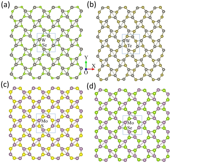
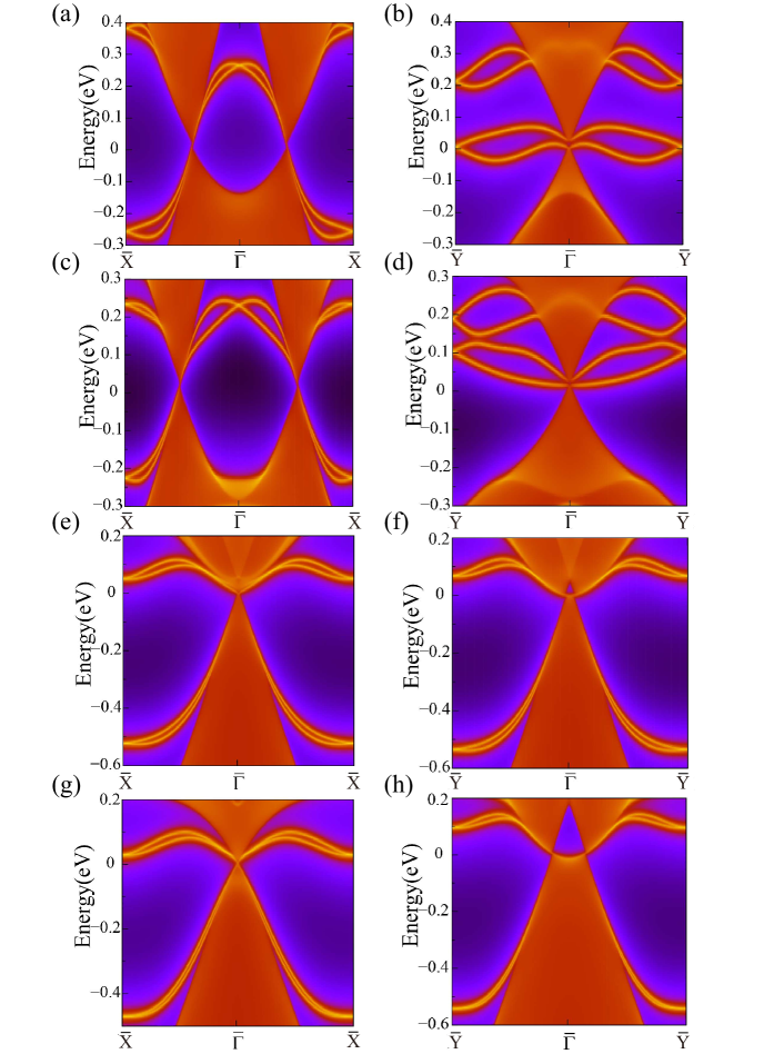
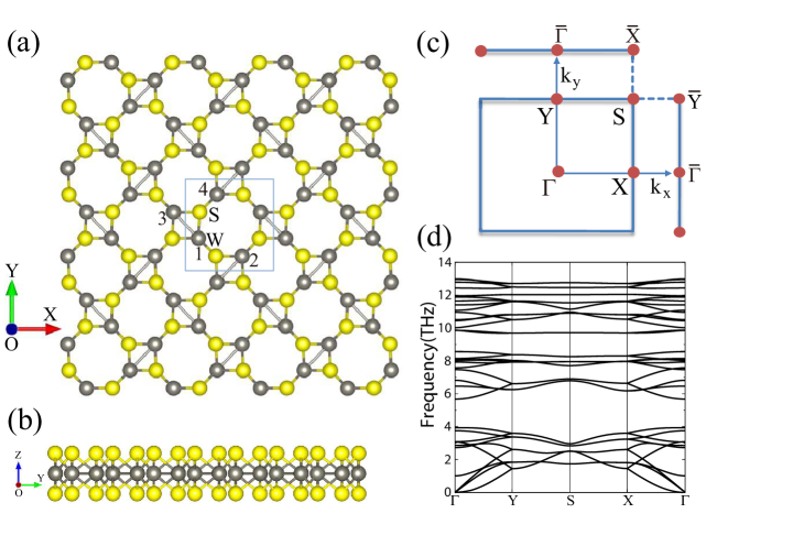
All TMD Haeckelites have the same non-symmorphic space group Pbam (). Except the difference of lattice constants, all other TMD Haeckelites have nearly the same properties as WS2. So we choose WS2-4-8 later as an example and the results of other TMD Haeckelites can be found in the Appendix. The relaxed crystal structure and Brillouin zone (BZ) for WS2-4-8 are shown in Fig. 1. It is noted that bond length between W 1 and 3 is reduced compared to that in honeycomb lattice. As we will see later, this bond is vital to topological phase transition. The dynamic stability of WS2-4-8 has been investigated by calculating it phonon spectrum. Imaginary frequencies can not be found in the phonon dispersion of WS2-4-8, which indicates the structure is stable (Fig. 1(d)).
| Structure | a(Å) | b(Å) | Gap(meV) | |
|---|---|---|---|---|
| WS2 | 6.34 | 6.41 | 53.82 | |
| WSe2 | 6.40 | 6.86 | 30.03 | |
| WTe2 | 6.65 | 7.38 | 14.743 | |
| MoS2 | 6.36 | 6.33 | 13.38 | |
| MoSe2 | 6.65 | 6.59 | 26.80 |
III results
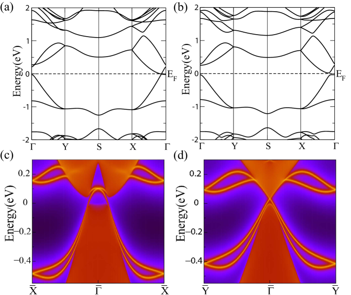
Both GGA and GGA+SOC band structures of WS2-4-8 are shown in Fig. 2. Along -X direction, there is a band crossing in GGA band structure. The little group of k point located on this direction is . The two crossing bands belong to different irreducible representations and such band crossing is protected by {} operation. When SOC is included, as we can see in Fig.2 (b), WS2-4-8 is a well defined insulator with indirect band gap around 53.8 meV. Gaps for other TMD Haeckelites are listed in the Table 1. For system possesses both time reversal (TR) and space inversion symmetry, the parity criterion proposed by Fu and Kane is a convenient method to judge its band topology number. Fu and Kane (2007) Since the space group of it is non-symmorphic, similar as that in single layer ZrTe5 and HfTe5 Weng et al. (2014b), all the bands at the three time reversal invariant momenta X, S, Y having degeneracy of even and odd states. Only the band inversion at can leads to nontrivial band topology. It is true that the total parity of occupied states at is -1 and the other three are +1. Therefore, the topological index equals to 1, which means WS2-4-8 is a QSH insulator. Considering the possible underestimation of band gap of GGA, non-local Heyd-Scuseria-Ernzerhof (HSE06) hybrid functionalHeyd et al. (2003); *heyd2006hybrid is further supplemented to check the topological property. The band topology does not change.
Since the existence of nontrivial edge states is the hallmark of QSH effect, we have calculated the edge states of WS2-4-8. As shown in Fig. 2 (c, d), there is edge Dirac cone dispersion connecting the bulk occupied and unoccupied states with Dirac point at for both X and Y edges.
In order to understand the band inversion process at point explicitly, a Slater-Koster TB has been constructed. Obviously, the main physics comes from the isolated group of four bands around the Fermi level. The band character and projected density of states (PDOS) analyses indicate that the low energy bands near the fermi level are mainly contributed by the and orbitals of W. The can mix with due to the distortion of 4-8 defects. For simplicity, only is taken into account for each W and one primitive cell contains four W atoms. Therefore, it is possible and reasonable to construct a TB hamiltonian for non-SOC case. The non-SOC TB hamiltonian with four localized bases (i=1, 2, 3, 4) can be written as follows in momentum space
| (5) |
where the hopping parameters are defined as
| (6) | |||
| (7) | |||
| (8) |
means the orbital on -th W atom labelled in Fig. 1 (a). However, one should note that periodic boundary condition is sacrificed here in order to get a concise form of Eq. (5). When the calculated properties concern global phase such as berry phase, we need to transform into another form which satisfies periodic boundary condition.
Similar to graphene, SOC is a second order effect for WS2-4-8. The intrinsic atomic SOC for W is of the order of 200 meV while it is about 4 meV for graphene. Compare to the extremely small gap for graphene, a large band gap (53.8 meV) is obtained for WS2-4-8 at last. The hybridization between and is zero due to symmetry. If TR symmetry is preserved, we will have . Therefore, even the hamiltonian size will be doubled when SOC is taken into account, we can still focus on spin up (spin down) subspace only. Spin down (spin up) subspace can be obtained using above restricted conditions. Considering all the symmetries, we obtain a generic matrix form for .
| (13) |
where and (pure imaginary numbers) are defined as
| (14) | ||||
| (15) |
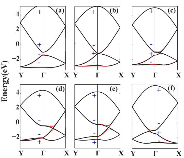
Only the total sign() makes sense. Sign can be inferred by inverting the whole bands of sign. So we take , and . As discussed above, only the band inversion at point can change the band topology. The four eigen states and their parities can be obtained explicitly as following:
| (16) | ||||
| (17) | ||||
| (18) | ||||
| (19) |
Obviously, the has the highest energy. The band inversion happens between and or and can lead to QSH state. That means the band inversion will exist as long as max(, ). Fig. 3 show the band structure calculated with the TB model with different sets of parameters. When (Fig. 3 (a)), the bonding and anti-bonding states are far away from each other. This is a trivial insulator. There will be a band touching at point if (Fig. 3 (b)). When , band inversion will happen (Fig. 3 (c)) and the system enters into QSH state. The two valence bands ( and ) with opposite parity will be degenerate at if (Fig. 3 (d)). When , they will separate each other (Fig. 3 (e)). Topological phase transition will not take place in this parametric region from Fig. 3(c) to (e), since the band inversion process occurs between two occupied valence bands. Another interesting thing is that and control the position of band crossing in non-SOC band structure. If , the crossing will be situated at direction (Fig. 3 (c)) and it will move to direction (Mo case in Appendix) for (Fig. 3 (f)).
Uniaxial strain effect has also been investigated with first-principles calculations, which can be used to tune the relative strength of these hopping parameters and control the topological quantum state transition. If we fix crystal constant and decrease , will increase faster than and . This means the band crossing in non-SOC band structure will move from to and uniaxial strain is always beneficial for band inversion. Similar results can be get for uniaxial strain along b-axis. Therefore the topology in WS2-4-8 is robust against uniaxial strain.
IV CONCLUSION
In summary, we have performed first-principles calculations for the electronic properties of TMD Haeckelites MX2-4-8 and found that they are 2D TIs. A simple TB model with one orbital per site and four sites per unit cell has been established to understand the band inversion mechanism. The nearest hopping parameter is vital to trigger the topological phase transition and can be tuned through lattice strain effect. Such simple square-like lattice model to achieve various topological quantum states is very stimulating. It will lead further study based on square lattice instead of honeycomb lattice and largely extend the searching range for topological materials.
Acknowledgements.
We acknowledge the supports from National Natural Science Foundation of China (No. 11274359 and 11422428), the 973 program of China (No. 2011CBA00108 and 2013CB921700) and the “Strategic Priority Research Program (B)” of the Chinese Academy of Sciences (No. XDB07020100).References
- Novoselov et al. (2004) K. S. Novoselov, A. K. Geim, S. V. Morozov, D. Jiang, Y. Zhang, S. V. Dubonos, I. V. Grigorieva, and A. A. Firsov, science 306, 666 (2004).
- Radisavljevic and Kis (2013) B. Radisavljevic and A. Kis, Nature materials 12, 815 (2013).
- Wang et al. (2012) Q. H. Wang, K. Kalantar-Zadeh, A. Kis, J. N. Coleman, and M. S. Strano, Nature nanotechnology 7, 699 (2012).
- Xu et al. (2014) G. Xu, J. Wang, B. Yan, and X.-L. Qi, Physical Review B 90, 100505 (2014).
- Shirodkar and Waghmare (2014) S. N. Shirodkar and U. V. Waghmare, Physical review letters 112, 157601 (2014).
- Cao et al. (2012) T. Cao, G. Wang, W. Han, H. Ye, C. Zhu, J. Shi, Q. Niu, P. Tan, E. Wang, B. Liu, et al., Nature communications 3, 887 (2012).
- Novoselov et al. (2005) K. S. Novoselov, D. Jiang, F. Schedin, T. J. Booth, V. V. Khotkevich, S. V. Morozov, and A. K. Geim, Proceedings of the National Academy of Sciences of the United States of America 102, 10451 (2005).
- Radisavljevic et al. (2011) B. Radisavljevic, A. Radenovic, J. Brivio, V. Giacometti, and A. Kis, Nature nanotechnology 6, 147 (2011).
- Eda et al. (2011) G. Eda, H. Yamaguchi, D. Voiry, T. Fujita, M. Chen, and M. Chhowalla, Nano letters 11, 5111 (2011).
- Coleman et al. (2011) J. N. Coleman, M. Lotya, A. O’Neill, S. D. Bergin, P. J. King, U. Khan, K. Young, A. Gaucher, S. De, R. J. Smith, et al., Science 331, 568 (2011).
- Lee et al. (2012) Y.-H. Lee, X.-Q. Zhang, W. Zhang, M.-T. Chang, C.-T. Lin, K.-D. Chang, Y.-C. Yu, J. T.-W. Wang, C.-S. Chang, L.-J. Li, et al., Advanced Materials 24, 2320 (2012).
- Liu et al. (2012) K.-K. Liu, W. Zhang, Y.-H. Lee, Y.-C. Lin, M.-T. Chang, C.-Y. Su, C.-S. Chang, H. Li, Y. Shi, H. Zhang, et al., Nano letters 12, 1538 (2012).
- Crespi et al. (1996) V. H. Crespi, L. X. Benedict, M. L. Cohen, and S. G. Louie, Physical Review B 53, R13303 (1996).
- Terrones et al. (2000) H. Terrones, M. Terrones, E. Hernández, N. Grobert, J.-C. Charlier, and P. Ajayan, Physical review letters 84, 1716 (2000).
- Sheng et al. (2012) X.-L. Sheng, H.-J. Cui, F. Ye, Q.-B. Yan, Q.-R. Zheng, and G. Su, Journal of Applied Physics 112, 074315 (2012).
- Li et al. (2014) W. Li, M. Guo, G. Zhang, and Y.-W. Zhang, Phys. Rev. B 89, 205402 (2014).
- Terrones and Terrones (2014) H. Terrones and M. Terrones, 2D Materials 1, 011003 (2014).
- van der Zande et al. (2013) A. M. van der Zande, P. Y. Huang, D. A. Chenet, T. C. Berkelbach, Y. You, G.-H. Lee, T. F. Heinz, D. R. Reichman, D. A. Muller, and J. C. Hone, Nature materials 12, 554 (2013).
- Kotakoski et al. (2011) J. Kotakoski, A. Krasheninnikov, U. Kaiser, and J. Meyer, Physical review letters 106, 105505 (2011).
- Komsa et al. (2012) H.-P. Komsa, J. Kotakoski, S. Kurasch, O. Lehtinen, U. Kaiser, and A. V. Krasheninnikov, Physical review letters 109, 035503 (2012).
- Qian et al. (2014) X. Qian, J. Liu, L. Fu, and J. Li, Science 346, 1344 (2014).
- Kane and Mele (2005) C. L. Kane and E. J. Mele, Physical Review Letters 95, 226801 (2005).
- Bernevig et al. (2006) B. A. Bernevig, T. L. Hughes, and S.-C. Zhang, Science 314, 1757 (2006).
- Yao et al. (2007) Y. Yao, F. Ye, X.-L. Qi, S.-C. Zhang, and Z. Fang, Physical Review B 75, 041401 (2007).
- König et al. (2007) M. König, S. Wiedmann, C. Brüne, A. Roth, H. Buhmann, L. W. Molenkamp, X.-L. Qi, and S.-C. Zhang, Science 318, 766 (2007).
- Knez et al. (2011) I. Knez, R.-R. Du, and G. Sullivan, Physical review letters 107, 136603 (2011).
- Weng et al. (2014a) H. Weng, X. Dai, and Z. Fang, MRS Bulletin 39, 849 (2014a).
- Liu et al. (2011) C.-C. Liu, W. Feng, and Y. Yao, Physical review letters 107, 076802 (2011).
- Xu et al. (2013) Y. Xu, B. Yan, H.-J. Zhang, J. Wang, G. Xu, P. Tang, W. Duan, and S.-C. Zhang, Phys. Rev. Lett. 111, 136804 (2013).
- Si et al. (2014) C. Si, J. Liu, Y. Xu, J. Wu, B.-L. Gu, and W. Duan, Phys. Rev. B 89, 115429 (2014).
- Song et al. (2014) Z. Song, C.-C. Liu, J. Yang, J. Han, M. Ye, B. Fu, Y. Yang, Q. Niu, J. Lu, and Y. Yao, arXiv:1402.2399 [cond-mat] (2014), arXiv:1402.2399 [cond-mat.mtrl-sci] .
- Zhou et al. (2014) J.-J. Zhou, W. Feng, C.-C. Liu, S. Guan, and Y. Yao, Nano Letters 14, 4767 (2014).
- Weng et al. (2014b) H. Weng, X. Dai, and Z. Fang, Physical Review X 4, 011002 (2014b).
- Luo and Xiang (0) W. Luo and H. Xiang, Nano Letters 0, null (0), http://dx.doi.org/10.1021/acs.nanolett.5b00418 .
- Blöchl (1994) P. E. Blöchl, Physical Review B 50, 17953 (1994).
- Kresse and Joubert (1999) G. Kresse and D. Joubert, Physical Review B 59, 1758 (1999).
- Kresse and Furthmüller (1996a) G. Kresse and J. Furthmüller, Computational Materials Science 6, 15 (1996a).
- Kresse and Furthmüller (1996b) G. Kresse and J. Furthmüller, Physical Review B 54, 11169 (1996b).
- Perdew et al. (1996) J. Perdew, K. Burke, and M. Ernzerhof, Phys. Rev. Lett. 77, 3865 (1996).
- Togo et al. (2008) A. Togo, F. Oba, and I. Tanaka, Physical Review B 78, 134106 (2008).
- Marzari and Vanderbilt (1997) N. Marzari and D. Vanderbilt, Physical review B 56, 12847 (1997).
- Souza et al. (2001) I. Souza, N. Marzari, and D. Vanderbilt, Physical Review B 65, 035109 (2001).
- Mostofi et al. (2008) A. A. Mostofi, J. R. Yates, Y.-S. Lee, I. Souza, D. Vanderbilt, and N. Marzari, Computer physics communications 178, 685 (2008).
- Sancho et al. (1984) M. L. Sancho, J. L. Sancho, and J. Rubio, Journal of Physics F: Metal Physics 14, 1205 (1984).
- Sancho et al. (1985) M. L. Sancho, J. L. Sancho, J. L. Sancho, and J. Rubio, Journal of Physics F: Metal Physics 15, 851 (1985).
- Fu and Kane (2007) L. Fu and C. Kane, Physical Review B 76, 045302 (2007).
- Heyd et al. (2003) J. Heyd, G. E. Scuseria, and M. Ernzerhof, The Journal of Chemical Physics 118, 8207 (2003).
- Heyd et al. (2006) J. Heyd, G. E. Scuseria, and M. Ernzerhof, The Journal of Chemical Physics 124, 219906 (2006).
V Appendix: Other TMD Haeckelites MX2-4-8
