Nonequilibrium spin texture within a thin layer below the surface of current-carrying topological insulator Bi2Se3: A first-principles quantum transport study
Abstract
We predict that unpolarized charge current injected into a ballistic thin film of prototypical topological insulator (TI) Bi2Se3 will generate a noncollinear spin texture on its surface. Furthermore, the nonequilibrium spin texture will extend into nm thick layer below the TI surfaces due to penetration of evanescent wavefunctions from the metallic surfaces into the bulk of TI. Averaging over few Å along the longitudinal direction defined by the current flow reveals large component pointing in the transverse direction. In addition, we find an order of magnitude smaller out-of-plane component when the direction of injected current with respect to Bi and Se atoms probes the largest hexagonal warping of the Dirac-cone dispersion on TI surface. Our analysis is based on an extension of the nonequilibrium Green functions combined with density functional theory (NEGF+DFT) to situations involving noncollinear spins and spin-orbit coupling. We also demonstrate how DFT calculations with properly optimized local orbital basis set can precisely match putatively more accurate calculations with plane-wave basis set for the supercell of Bi2Se3.
pacs:
72.25.Dc, 75.70.Tj, 71.15.Mb, 72.10.BgThe newly discovered three-dimensional topological insulator (3D TIs) materials possess a usual band gap in the bulk while also hosting metallic surfaces. The low-energy quasiparticles on these surfaces behave as massless Dirac fermions whose spins are locked to their momenta due to strong spin-orbit coupling (SOC). Hasan2010 Such spin-momentum locking is viewed as a resource for spintronic applications. Pesin2012 For example, very recent experiments Mellnik2014 have demonstrated magnetization dynamics of a single ferromagnetic metallic (FM) overlayer deposited on the surface of 3D TIs due to current-induced SO torques. Another recent experiment Shiomi2014 has detected spin-to-charge conversion Mahfouzi2014a ; Shen2014 when precessing magnetization of the FM overlayer pumps pure spin current into the metallic surface of 3D TIs.
The microscopic mechanism behind these phenomena can be traced to the so-called Edelstein effect (EE), originally predicted Edelstein1990 for a diffusive two-dimensional electron gas (2DEG) with the Rashba SOC Winkler2003 and observed much later experimentally. Kato2004 In the EE in 2DEG, longitudinal unpolarized charge current flowing along the -axis drives a homogeneous nonequilibrium spin density pointing in the transverse direction. The diffusive metallic surface of TIs also exhibits EE where a current-driven spin density is substantially enhanced Pesin2012 (by a factor , with being the Fermi velocity in TI and is the strength Winkler2003 of the Rashba SOC in 2DEG). This enhancement can be explained by the spin-momentum locking along the single Fermi circle, Hasan2010 formed in -space at the intersection of the Dirac cone energy-momentum dispersion and the Fermi energy plane, in contrast to spin-momentum locking along the two circles Winkler2003 in the case of Rashba 2DEG which counter the effect of each other. This has motivated recent experiments Li2014 probing directly in three-terminal geometry where nonmagnetic electrodes inject unpolarized charge current into a TI, while a third FM contact deposited in the middle of the top surface of the TI film detects a voltage signal when a non-zero is induced. These setups quantify the projection of onto the magnetization of the third FM contact.
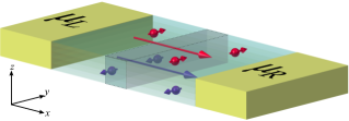
However, this picture of EE on the surface of TI is based on simplistic model Hamiltonians. Mellnik2014 ; Pesin2012 Here we employ first-principles quantum transport approach to analyze microscopic details, over Å length scale, of current-driven in the two-terminal ballistic thin film geometry hosting realistic TI material, as illustrated in Fig. 1. We choose Bi2Se3 as the prototypical TI material—with its single Dirac cone in the surface band structure, relatively large bulk band gap, and Dirac point (DP) inside the gap [see Fig. 4(a)]—on which many recent experiments probing EE directly Li2014 or indirectly Mellnik2014 ; Shiomi2014 have been performed. The central region of the device in Fig. 1, which has length Å along the -axis and infinite width along the -axis, is attached to two semi-infinite electrodes made of the same material. The electrodes are assumed to terminate at infinity into macroscopic Fermi liquid reservoirs where electrons are thermalized to acquire electrochemical potential in the left reservoir and in the right one. The Hamiltonian of the central region and the electrodes is obtained from the noncollinear density functional theory (ncDFT), implemented by us in ATK package atk , using optimized pseudo-atomic localized basis functions Ozaki2003 and SOC introduced via the total-angular-momentum-dependent pseudopotentials. Theurich2001 The transport properties of the system in Fig. 1 are computed using the nonequilibrium Green function (NEGF) formalism, Stefanucci2013 so that our approach represents an extension of the widely used NEGF+DFT framework Taylor2001 to transport problems involving noncollinear spins and SOC.
In the simplest picture—based on effective Hamiltonian ( is the vector of the Pauli matrices; is the momentum operator; and is the unit vector along the -axis in Fig. 1) describing massless Dirac electrons on the metallic surfaces of TIs—the spin and momentum of electronic eigenstates are orthogonal to each other along the single Fermi circle. This generates net homogeneous after an applied electric field shifts the Fermi circle Pesin2012 ; Mellnik2014 ; Misawa2011 along the momentum parallel to . Such manifestation of EE persists in ballistic samples as well Modak2012 ; Chang2014a where there is no electric field within the TI but instead one applies bias voltage to inject a current into the TI, as illustrated in Fig 1. The relations or describing EE in the diffusive or ballistic transport regimes, respectively, are allowed only in nonequilibrium since in equilibrium changes sign under time reversal, and, therefore, has to vanish (assuming absence of magnetic field).
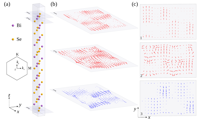
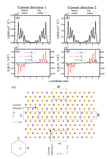
This simplistic picture can be contrasted with our principal results in Figs. 2 and 3. When a small (ensuring linear-response transport regime) is applied between the reservoirs in Fig. 1, the unpolarized charge current injected into Bi2Se3 thin film generates a nonequilibrium whose complex noncollinear texture within three planes selected in Fig. 2(a) is plotted in Figs. 2(b) and 2(c). For the visualization we use real-space grid for whose spacing is Å. Furthermore, Figs. 2 and 3 demonstrate that nonequilibrium spin texture will appear not only on the TI surface, but also within nm thick layer of its bulk just below the top and bottom surfaces. This feature is explained in Figs. 3(a) and 3(b) showing spatial profile of the local density of states (LDOS) at the Fermi energy over the cell depicted in Fig. 1. The non-zero LDOS and the corresponding in the bulk of the TI thin film stem from evanescent wavefunctions which originate from the top and bottom metallic surfaces and penetrate into the energy gap of the insulating bulk. The Bi2Se3 is a strongly anisotropic material composed of quintuple layers (QLs) of Bi and Se atoms, illustrated in Fig. 2(a), where one QL consists of three Se layers strongly bonded to two Bi layers in between. For Bi2Se3 film thinner than 5 QLs, the evanescent wavefunctions from the top and bottom metallic surface can overlap to create a minigap Yazyev2010 ; Park2010 at the DP. We select the thickness of Bi2Se3 to be 5 QLs along the -axis in Fig. 1, which ensures that the LDOS in Figs. 3(a) and 3(b) goes to zero on the plane half way between the top and bottom surfaces of the TI thin film.
Upon averaging nonequilibrium over a Å long cell depicted in Fig. 1, we obtain spatial profiles in Figs. 3(c) and 3(d) which show that is the largest component independently of the direction of incoming electrons. An order of magnitude smaller component shown in Fig. 3(d) appears for electrons incoming along current direction 2 marked in panel (e). This is in accord with experiments in equilibrium where spin- and angle-resolved photoemission spectroscopy Pan2011 finds largest out-of-plane spin component along the corresponding direction in the 2D Brillouin zone (BZ). This is due to hexagonal warping of the Dirac cone surface band structure, as confirmed by DFT calculations Yazyev2010 ; Zhao2011 finding that equilibrium expectation value of spin in the eigenstates of Bi2Se3 surfaces tilts out of the 2D BZ. Thus, Fig. 3 offers a novel prescription for probing hexagonal warping even close to DP via transport measurements where charge current is injected in different directions relative to the orientation of the lattice of Bi and Se atoms.
We now explain the technical details of our calculations. The extension of DFT to the case of spin-polarized systems is formally derived in terms of total electron density and vector magnetization density . In the collinear DFT, points in the same direction at all points in space, which is insufficient to study magnetic systems where the direction of the local magnetization is not constrained to a particular axis or systems governed by SOC. In ncDFT, Capelle2001 the exchange-correlation (XC) functional depends on pointing in arbitrary directions. The local density approximation(LDA) and most often employed version of generalized gradient approximation (GGA), implemented also by us in ATK, atk make additional approximations Capelle2001 that lead to the XC magnetic field being parallel everywhere to .
The single-particle spin-dependent Kohn-Sham (KS) Hamiltonian in ncDFT takes the form
| (1) |
where , and are the Hartree, external and XC potential, respectively. Diagonalization of proceeds by approximating the Hilbert space of all single-electron eigenfunctions with a finite set of basis functions. A popular basis set is plane-waves (PWs), where varying only one parameter (the energy cutoff) allows one to improve the basis systematically. Linear combination of atomic orbitals (LCAO) basis sets require more tuning, however, they simplify the NEGF calculations Taylor2001 where one has to spatially separate system into the central region and semi-infinite electrodes, as illustrated in Fig. 1.
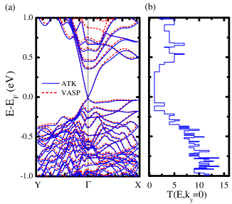
Since the pioneering screening Zhang2009 of candidate TI materials via ncDFT calculations, their electronic band structure has most often been calculated Yazyev2010 ; Park2010 using PW ncDFT with electron-core interactions described via projector augmented wave (PAW) method. Blochl1994 In Fig. 4(a) we demonstrate that such calculations, performed by VASP package, Kresse1993 can be accurately reproduced by pseudopotential-based LCAO ncDFT implemented in ATK. atk The supercell considered in both calculations is shown in Fig. 2(a), which includes 5 QLs terminated by Se atomic layer on both the top and bottom surface, as well as Å thick vacuum layer above and below these Se atomic layers.
We note that previous attempts Zhao2011 to apply pseudopotential-based LCAO ncDFT to Bi2Se3 have yielded either poor accuracy of its electronic band structure (e.g., compare our Fig. 4(a) with Fig. 1 in Ref. Zhao2011, ) or have required intricate fine tuning. Rivera2014 Therefore, we provide here a complete recipe for the proper usage of LCAO ncDFT to reproduce Fig. 4(a). In ATK calculations in Fig. 4(a), the electron-core interactions are described by norm-conserving pseudopotentials. The pseudopotentials are obtained by mapping the solution of the Dirac equation, which naturally includes SOC, Theurich2001 to non-relativistic pseudopotential, , with local contribution and non-local contributions from the total angular momentum and . The non-local terms are expanded in terms of SO projector functions, , where are normalization constants and the indices denote the possible spin orientations . We use Perdew-Burke-Ernzerhof (PBE) parametrization of GGA for the XC functional and a LCAO basis set generated by the OpenMX package, openmx ; Ozaki2003 which consists of s2p2d1 orbitals on Se atoms and s2p2d2 on Bi atoms. These pseudoatomic orbitals were generated by a confinement scheme Ozaki2003 with the cutoff radius 7.0 a.u. and 8.0 a.u. for Se and Bi atoms, respectively. The energy mesh cutoff for the real-space grid is chosen as 75.0 Hartree. In VASP calculations Kresse1993 in Fig. 4(a), the electron-core interactions are described by PAW method, Blochl1994 and we employ PBE GGA for the XC functional. The cutoff energy for the PW basis set is 350 eV. In both ATK and VASP calculations we employ -point mesh within Monkhorst-Pack scheme for the BZ integration.
The eigenstates of the KS Hamiltonian in Eq. (1) make it possible to construct the equilibrium density matrix for electrons at and temperature described by the Fermi distribution function . The local electron and magnetization density, as the central variables of ncDFT, are obtained from and , where the trace is taken over the spin Hilbert space.
In steady-state nonequilibrium due to dc current flowing between the left and right reservoirs in Fig. 1, we construct the nonequilibrium density matrix Mahfouzi2013 using NEGFs:
| (2) |
This yields plotted in Figs. 2 and 3. The NEGF formalism Stefanucci2013 for steady-state transport operates with two central quantities—the retarded GF, , and the lesser GF, —which describe the density of available quantum states and how electrons occupy those states, respectively. In the absence of inelastic processes, these are given by and . Here the self-energies are due to semi-infinite electrodes, and is the level broadening matrix. For the chosen LCAO basis set, the Hamiltonian matrix is composed of elements and the overlap matrix is composed of elements . In the linear-response transport regime considered here, Eq. (2) can be expanded Mahfouzi2013 to first order in bias voltage . Since is zero in equilibrium (because of assumed absence of external magnetic field), the linear-response density matrix can be simplified to, Mahfouzi2013 . Otherwise, the gauge-invariant form of requires additional terms Mahfouzi2013 to properly remove the equilibrium expectation value of a considered physical quantity.
The retarded GF also allows us to obtain the transmission function of the device in Fig. 1, , which depends on energy and transverse momentum due to assumed periodicity in the -direction. The total transmission function is obtained by integrating over , which determines the linear-response conductance via the Landauer formula, . We confirm in Fig. 4(b) that for within the bulk gap shown in Fig. 4(a) because only one doubly degenerate helical conducting channel is open for transport in that energy range Wang2012c for injected electrons with momentum along the –M direction ().
In conclusion, using NEGF+ncDFT framework implemented by us in ATK package, atk we computed a nonequilibrium spin texture within a thin film of current-carrying Bi2Se3 TI material. The non-zero texture appears on the TI metallic top and bottom surfaces, as well as within bulk layers of thickness nm below the surfaces that effectively dope the bulk by evanescent wavefunctions. The spin texture is noncollinear and complex on length scales Å. Upon averaging it over a few Å we find a simpler pattern—with either , or where —depending on the direction of injected current with respect to orientation of the lattice of Bi and Se atoms. Such dependency offers a novel probe, via electronic transport measurements, Li2014 of the hexagonal warping of the Dirac cone surface band structure. For the envisaged spintronic applications of TIs, it is essential to understand how changes due to finite bias voltage or self-consistent coupling Semenov2014 to magnetization of a ferromagnetic (metal or insulator) overlayer, which we relegate to future studies.
Acknowledgements.
P.-H. C. and B. K. N. were supported by NSF Grant No. ECCS 1509094. The supercomputing time was provided by XSEDE, which is supported by NSF Grant No. ACI-1053575. QuantumWise acknowledges support from the Danish Innovation Fund Grant No. 79-2013-1: “Nano-scale design tools for the semiconductor industry.”References
- (1) M. Z. Hasan and C. L. Kane, Rev. Mod. Phys. 82, 3045 (2010); X.-L. Qi and S.-C. Zhang, ibid. 83, 1057 (2011).
- (2) D. Pesin and A. H. MacDonald, Nature Mater. 11, 409 (2012).
- (3) A. R. Mellnik et al., Nature 511, 449 (2014); Y. Fan et al., Nature Mater. 13, 699 (2014).
- (4) Y. Shiomi et al., Phys. Rev. Lett. 113, 196601 (2014).
- (5) F. Mahfouzi, N. Nagaosa, and B. K. Nikolić, Phys. Rev. B 90, 115432 (2014).
- (6) K. Shen, G. Vignale, and R. Raimondi, Phys. Rev. Lett. 112, 096601 (2014).
- (7) V. M. Edelstein, Solid State Comm. 73, 233 (1990); A. G. Aronov and Y. B. Lyanda-Geller, JETP Letters 50, 431 (1989).
- (8) R. Winkler, Spin-Orbit Coupling Effects in Two-Dimensional Electron and Hole Systems (Springer, Berlin, 2003).
- (9) Y. Kato, R. C. Myers, A. C. Gossard, and D. D. Awschalom, Phys. Rev. Lett. 93, 176601 (2004); A. Y. Silov et al., Appl. Phys. Lett. 85, 5929 (2004); S.D. Ganichev et al., J. Magn. Magn. Mater. 300,127 (2006).
- (10) C. H. Li et al., Nature Nanotech. 9, 218 (2014); Y. Ando et al., Nano Letters 14, 6226 (2014); L. Liu, A. Richardella, I. Garate, Y. Zhu, N. Samarth, C.-T. Chen, Phys. Rev. B 91, 235437 (2015); J. Tian, I. Miotkowski, S. Hong, and Y. P. Chen, arXiv:1501.05050.
- (11) Atomistix ToolKit (ATK) 2014.2, http://www.quantumwise.com.
- (12) T. Ozaki, Phys. Rev. B 67, 155108 (2003); T. Ozaki and H. Kino, Phys. Rev. B 69, 195113 (2004).
- (13) G. Theurich and N. A. Hill, Phys. Rev. B 64, 073106 (2001).
- (14) G. Stefanucci and R. van Leeuwen, Nonequilibrium Many-Body Theory of Quantum Systems: A Modern Introduction (Cambridge University Press, Cambridge, 2013).
- (15) J. Taylor, H. Guo, and J. Wang, Phys. Rev. B 63, 245407 (2001); M. Brandbyge et al., Phys. Rev. B 65, 165401 (2002); D. A. Areshkin and B. K. Nikolić, Phys. Rev. B 81, 155450 (2010).
- (16) T. Misawa, T. Yokoyama, and S. Murakami, Phys. Rev. B 84, 165407 (2011).
- (17) S. Modak, K. Sengupta, and D. Sen, Phys. Rev. B 86, 205114 (2012).
- (18) P.-H. Chang, F. Mahfouzi, N. Nagaosa, and B. K. Nikolić, Phys. Rev. B 89, 195418 (2014).
- (19) O. V. Yazyev, J. E. Moore, and S. G. Louie, Phys. Rev. Lett. 105, 266806 (2010).
- (20) K. Park, J. J. Heremans, V. W. Scarola, and D. Minic, Phys. Rev. Lett. 105, 186801 (2010).
- (21) Y. Zhao et al., Nano Lett. 11, 2088 (2011).
- (22) Z.-H. Pan et al., Phys. Rev. Lett. 106, 257004 (2011); M. Nomura et al., Phys. Rev. B 89, 045134 (2014).
- (23) K. Capelle, G. Vignale, and B. L. Györffy, Phys. Rev. Lett. 87, 206403 (2001); F. G. Eich, S. Pittalis, and G. Vignale, Phys. Rev. B 88, 245102 (2013).
- (24) H. Zhang et al., Nature Phys. 5, 438 (2009).
- (25) P. E. Blöchl, Phys. Rev. B 50, 17953 (1994); G. Kresse and D. Joubert, Phys. Rev. B 59, 1758 (1999).
- (26) P. Rivera et al., Comput. Mater. Sci. 98, 372 (2015).
- (27) G. Kresse and J. Hafner, Phys. Rev. B 47, 558 (1993); G. Kresse and J. Furthmüller, Phys. Rev. B 54, 11169 (1996); G. Kresse and J. Furthmüllerb, Comput. Mater. Sci. 6, 15 (1996).
- (28) http://www.openmx-square.org/.
- (29) F. Mahfouzi, N. Nagaosa, and B. K. Nikolić, Phys. Rev. Lett. 109, 166602 (2012); F. Mahfouzi and B. K. Nikolić, SPIN 3, 1330002 (2013).
- (30) X.-F. Wang, Y. Hu, and H. Guo, Phys. Rev. B 85, 241402 (2012); A. Narayan, I. Rungger, A. Droghetti, and S. Sanvito, Phys. Rev. B 90, 205431 (2014).
- (31) Y. G. Semenov, X. Duan, and K. W. Kim, Phys. Rev. B 89, 201405 (2014).