Magnetic microscopy of topologically protected homochiral domain walls in an ultrathin perpendicularly magnetized Co film
Abstract
Next-generation concepts for solid-state memory devices are based on current-driven domain wall propagation, where the wall velocity governs the device performance. It has been shown that the domain wall velocity and the direction of travel is controlled by the nature of the wall and its chirality. This chirality is attributed to effects emerging from the lack of inversion symmetry at the interface between a ferromagnet and a heavy metal, leading to an interfacial Dzyaloshinskii-Moriya interaction that can control the shape and chirality of the magnetic domain wall. Here we present direct imaging of domain walls in Pt/Co/AlOx films using Lorentz transmission electron microscopy, demonstrating the presence of homochiral, and thus topologically protected, Néel walls. Such domain walls are good candidates for dense data storage, bringing the bit size down close to the limit of the domain wall width.
The broken inversion symmetry at interfaces between ferromagnets and heavy (high spin-orbit interaction) metals offers new ways to manipulate the magnetic state. The combination of a heavy metal and a thin ferromagnetic film gives rise to new phenomena which normally vanish in the bulk, but play an important role as soon as the thickness of the ferromagnet is reduced to an atomic size. The presence of a Rashba electric fieldMiron_Nature2010 and Dzyaloshinskii-Moryia interactionchen2013tailoring (DMI) have been recently demonstrated in such systems. Therefore the classical picture of magnetism as being an interplay between exchange, dipolar, and anisotropy energies is perturbed by a new energy term with very significant and profound consequences. This DMI term is expressed as , where is the DMI vector, and and are spin moments sitting on neighbouring atoms. When is sufficiently strong, a non-uniform ferromagnetic state has a lower energy giving rise to exotic structures such as cycloidsferriani2008atomic , helicesrossler2006spontaneous , or skyrmions heinze2011spontaneous as the magnetic ground state: at an interface the DMI enforces spin textures of a cycloidal formfert1991magnetic ; Crepieux1998 ; Freimuth2014 . However, for small DMI values, domain walls (DWs) are the precursors of these non-uniform states. Here the DMI strength is imprinted into the static DW texture via a virtual effective magnetic field that prefers a Néel wall of a given chirality rather than the magnetostatically cheaper Bloch wall. It has been shown that the choice of the heavy element dictates the sign and magnitude of the DMIryu2014chiral ; hrabec2014measuring ; chen2013tailoring ; torrejon2014interface . The nature of the DW has remarkable consequences for the processes of DW dynamicsde2013piezoelectric and the sensitivity of the DW to the torques exerted on the localized magnetic momentskhvalkovskiy2013matching . The DW texture can be deduced indirectly by matching models with current-emori2013current ; ryu2013chiral ; conte2014interfacial and field-inducedThiaville_DMI ; choe ; hrabec2014measuring DW displacement data.
Determination of the DW structure is therefore a key part of any investigation in these materials. Historically, imaging of DWs in films with planar magnetization is well established with many examples demonstrating the capability of imaging DWs which have widths upwards of tens to hundreds of nm. Methods such as magnetic force microscopyyamaguchi2004real , photoemission electron microscopyklaui2004head , electron holographybackes2007transverse , or Lorentz transmission electron microscopybasith2011direct (L-TEM) have been used to image such DWs. The spatial extent of DWs in materials with out-of-plane anisotropy is often only 10 nm or less, making them interesting objects for high density data storage devices. Resolving such small magnetic objects is a challenge but a number of methods, including those listed above, are suitable for such studies. Spin-polarized scanning tunnelling microscopyKubetzka_2003 and spin-polarized low energy electron microscopychen2013tailoring manifested the Néel texture of the walls in bilayer systems grown and studied in situ, while nitrogen-vacancy microscopy revealed and demonstrated the difference of the stray field distribution above the Bloch and Néel walls in trilayer systems such as Pt/Co/AlOx or Pt/Co/Pttetienne2014nature . Pt/Co/AlOx system is extremely interesting for solid state memory devicesparkin2008magnetic due to the combination of high DW velocitiesMoore_APL2008 ; moore2009erratum (with various phenomena being proposed to explain this processMiron_Nature2010 ; haazen2013domain ; Pizzini_DMI ) with the oxide layer which can be used as a tunnel barrier for the information read-out. Here we use L-TEM to directly image DWs in perpendicularly magnetized ‘device-ready’ films of Pt/Co/AlOx, allowing us to deduce the presence of narrow homochiral Néel walls. Furthermore, measurements taken using both L-TEM and polar Kerr imaging, which demonstrate the topological protection of these walls when they are forced together by a field, are consistent with the presence of a measurable DMI.
Results

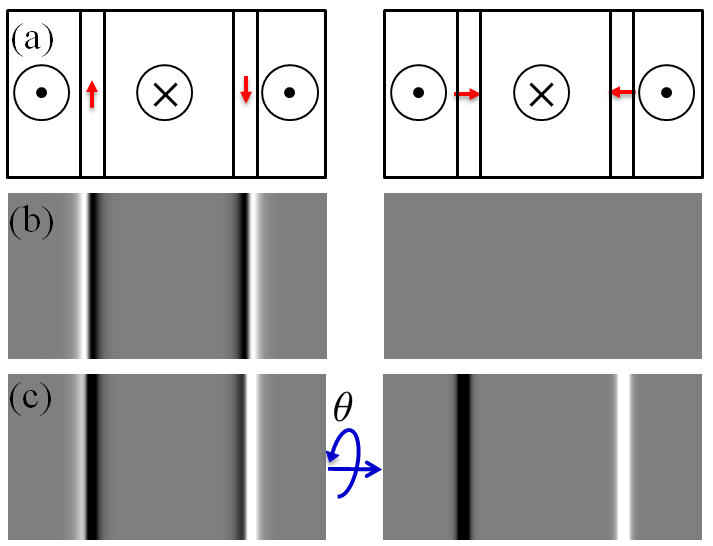
The two main types of DWs for films possessing out-of-plane anisotropy, Bloch and Néel, are sketched in figure 1(a) in plan view. The Bloch wall creates charges only at the top and bottom edges of the film, which are well separated for walls of any significant length, but is divergence-free otherwise. In contrast to this, the Néel wall gives rise to positive and negative magnetic charges along the whole length of the DW, separated by the DW width , which is of the order of , where is the exchange stiffness and is the anisotropy constant. Thus the Bloch wall is energetically favoured in perpendicularly magnetized thin films on magnetostatic grounds. To rotate the magnetic moments from the Bloch into the Néel configuration, an in-plane anisotropy expressed as , where is the demagnetizing factortarasenko that depends on the DW width and film thickness , has to be overcome. This can be achieved either by applying an external magnetic field in the -directionhaazen2013domain , or by an effective magnetic field arising from the DMIThiaville_DMI .

To enable observation of the DWs, Fresnel-mode L-TEM imaging was carried out, which reveals DWs as lines of black/white contrastchapman1984investigation . For materials with in-plane magnetization this is achieved by defocussing the imaging lens; the induction either side of the DW results in a Lorentz deflection and the electron beam diverges or converges at the wall giving dark or bright wall contrast. However, for perpendicularly magnetized films, no deflection arises from the out-of-plane component if the electron beam is at normal incidence. Thus any contrast will arise from the in-plane component, which only exists at the position of the DW. For the case of Bloch and Néel DWs, the calculated Fresnel images are shown in figure 1(b) for normal incidence. The Bloch wall on the left shows black/white contrast as each edge of the DW is similar a diverging or converging wall, but with no induction on one side of the wall, as has been observed experimentally masseboeuf2009lorentz . In the case of Néel walls at normal incidence no contrast is visible, as shown in the right hand image of figure 1(b) calculated from the magnetization configuration. The reason for this is that the wall rotation is completely divergent in nature and gives no contrast in Lorentz microscopy. The basis of contrast in Lorentz microscopy is that the magnetization configuration must have a component of magnetization curl parallel to the electron beam direction mcvitie2006quantitative ; there is no such component present in the Néel wall. This distinguishes the two walls, although the Néel walls are invisible in this orientation.
The Néel wall can be made visible by tilting the film along an axis perpendicular to the wall in the plane of the film so that the electron beam no longer passes through the film at normal incidence. This then results in a component of magnetization/induction in the domains that is perpendicular to the beam and gives only black or only white contrast at the walls, as shown in figure 1(c) on the right hand side. Tilting of a film with a Bloch wall results in contrast observed in figure 1(c) on the left, which retains its black/white character although now in an asymmetric form. In this way the wall positions are identified and their forms distinguished. In summary, Bloch walls will be visible when the film is untilted and show asymmetric black/white contrast when tilted, whilst Néel walls will be invisible when untilted but show symmetric black or white contrast when tilted.

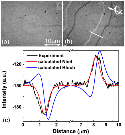
The walls under investigation here in sputtered Pt/Co/AlOx trilayers were imaged in the Fresnel mode, and the results are shown in figure 2. First, the film was subjected to an out-of-plane applied field of mT using the objective lens, close to value of the coercivity, to induce DWs. After the applied field had been removed, Fresnel images were taken both untilted and tilted by 30 degrees, which are shown in figure 2(a) and (b), respectively. It is apparent that no DWs at all are visible when the film is untilted, furthermore when tilted the DW contrast appears either dark or bright without any dark/bright asymmetry. An intensity linetrace across bright and dark walls is shown in figure 2(c) confirming the symmetric nature of the contrast. (A small intensity variation across the image can be seen in both images which is non magnetic in origin). To illustrate the difference between Bloch and Néel walls, calculated intensity variations derived from the tilted images in figure 1(c) are shown in figure 2(c) for comparison with the data. The clear asymmetry expected from the Bloch walls is not visible in the experimental linetrace. We conclude therefore that the walls are of the Néel type. It should be noted that the component of the magnetization at the centre of the Néel wall gives no contrast in Fresnel images in this configuration. Therefore, whilst we can conclude that these are indeed Néel walls, it is not possible to say anything about the chirality from such images alone. We now turn our attention to the domain wall behaviour in the presence of an applied field to determine whether chiral effects are induced by the asymmetric interfaces of the Co layer.
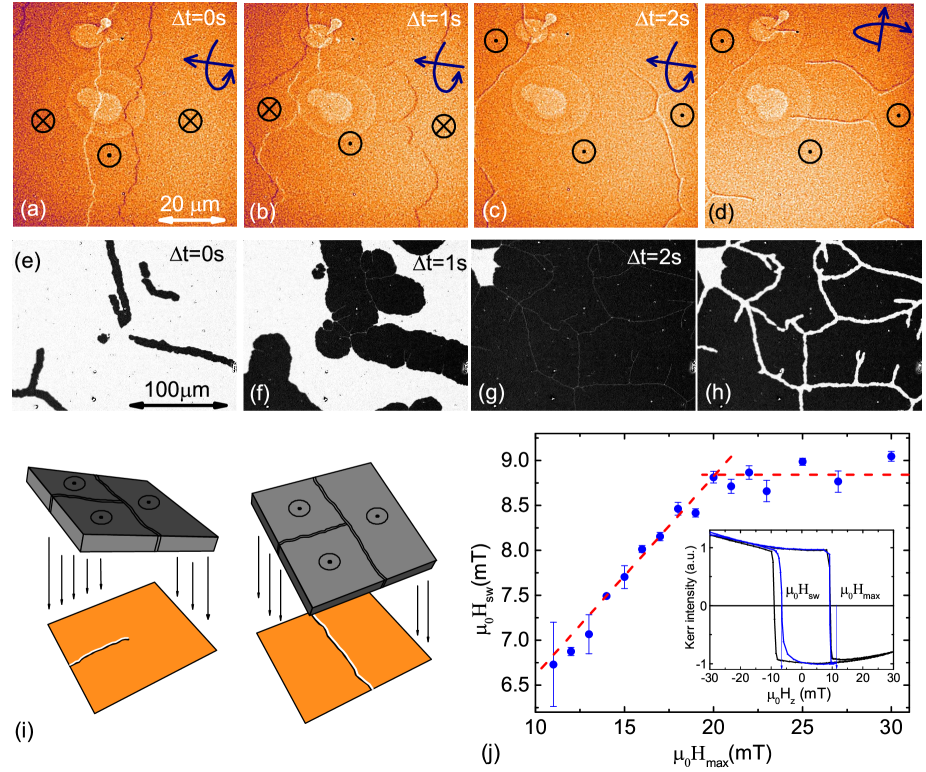
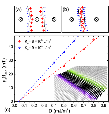
The nature of the DW chiral handedness was studied in the TEM by varying the objective lens field (which is vertical) to bring the DWs together and observing the subsequent interaction between them. Figure 3(a)-(c) shows a sequence of images of DWs displaced by a magnetic field. The initial magnetic state shown in figure 3(a) is imaged before the magnetic field is applied. Figure 3(b) and (c) show the magnetic state during and after the application of a magnetic field mT. Figure 3(d) was acquired under the same conditions as figure 3(c), but for a different in-plane tilt direction as depicted schematically in figure 3(i), confirming the Néel state. It can be seen that the up-domain state grows and the down-domain shrinks until the point where the two DWs meet, at which point they merge into 360∘ DWs. A much larger magnetic field has to be applied in order to annihilate these and fully saturate the film. The formation of 360∘ DWs takes place when two DWs of the same chirality meet and are unable to annihilate for topological reasons hubertandschaefer . Since both DWs have the same chirality, the magnetostatic charge created on either side of the wall prevents the two walls, which are locked and protected by the DMI, from annihilation. This situation is sketched in figure 4(a)-(b). It is important to note that all of the DW pairs we observed formed 360∘ DWs when they met, showing that these Néel walls are homochiral, a situation that is enforced by the presence of an interfacial DMI.

To overcome this topological protection alejos2015micromagnetic , a sufficiently strong magnetic field must be applied to overcome the energy barrier and annihilate the DW. Measuring the field required to do this has been suggested as a means of experimentally determining the strength of the DMI Hiramatsu2014 . To collect a statistically significant number of annihilation events, we have mimicked the same experiment with Kerr microscopy measurements in which the up and down domains are easily visible as dark or bright contrast. Domain expansion upon the application of a magnetic field is shown in the Kerr micrographs figure 3(e)-(g), exhibiting the same behaviour that was observed by the L-TEM. The white lines appearing in figure 3(g) correspond to the two Néel walls squeezed together into a structure. Since the magnetic field is not large enough to annihilate them, it is possible to pull them apart again by applying a small magnetic field of the opposite polarity as depicted in figure 3(h). The coercive field mT can be extracted from the Kerr effect hysteresis loop shown inset in figure 3(j), measured with the magnetic field swept in the range mT.
In order to measure the annihilation field, the following magnetic field sequence, illustrated by the blue curve in the inset of figure 3(j), was performed. The film was first saturated at mT and then the magnetic field was ramped to a maximum field above the coercive field. The magnetic field is then swept back to mT and so the switching field can be measured. It is clear from the figure 3(j) inset that the film now switches at a field that is lower than the coercive field of the major loop, i.e. .
Figure 3(j) shows the dependence of the switching field on the maximum field . The switching field rises linearly until it is as large as , which occurs at mT. For larger than this, . The linear rise is caused by a greater proportion of annihilated walls, which leads to a lower number of pre-nucleated regions for subsequent reverse domain growth on the reverse portion of the field sweep and a higher switching field. Once all the DWs are annihilated at mT, the reversal process is governed by reversed domain nucleation and propagation—just as on the major loop—rather than propagation alone. Since the stability of the two Néel walls in the 360∘ structure depends on the magnitude of the DMI, the annihilation field is a direct evaluation of the magnitude of the DMIHiramatsu2014 .
Micromagnetic simulations were performed to evaluate the effect of the DMI on the DW annihilation field. In this model we used the following material parameters appropriate to Co: saturation magnetization A/m, exchange stiffness pJ/m, and perpendicular uniaxial anisotropy J/m3. To investigate this problem we first prepared two DWs in a simulated nanowire of lateral dimensions nm nm by introducing an up-down-up domain. The two DWs were set to be 300 nm apart and then brought together by an external field as shown in the inset of figure 4(c). Figure 4(c) shows the calculated dependence of the annihilation field on for different anisotropies to include the error of the anisotropy measurement. We find that our measured value of implies that mJ/m2. Since the micromagnetic simulations were performed at K, and there is a possibility of DW annihilation due to thermal activation, this value is only a lower limit of . The real could be much be higher, potentially reaching similar value mJ/m2 as measured by Pizzini et al. Pizzini_DMI . In any case, the most pessimistic value of mJ/m2 is already high enough satisfy the condition needed to enforce the Néel configuration for the DWs in this system Thiaville_DMI .
Summary
Our L-TEM experiments show that DWs in the Pt/Co/AlOx system are indeed of the Néel form, enforced by an interfacial DMI overcoming the preference of the magnetostatic energy term for Bloch walls. The fact that they always form structures when pressed together by a field shows that these walls are homochiral, just as is expected in the presence of a DMI. We have implemented the method of annihilating these structures with a field in order to estimate the strength of the DMI in this system as being at least mJ/m2. This confirms the widespread assumption, made to interpret field- or current-driven domain wall motion data, that such walls are of the Néel type due to an effective field arising from the interfacial DMI. Knowledge of wall structures is not only important in DW dynamics experiments and the design of spintronic technologies based on this phenomenon, such as racetrack memories, where the fact that the DWs are topologically protected from mutual annihilation means that they can be very closely packed, permitting data density. Also, these Néel type walls, wrapped in a circle, form the boundaries of bubble domains with non-zero skyrmion winding numbers, leading to inertial dynamics Buttner2015 and with potential for use in skyrmion-based spintronic devices Nagaosa2013 ; Fert2013 .
Methods
Trilayer films of Ta(3.2 nm)/Pt(3 nm)/Co(0.8 nm)/AlOx(3 nm) were deposited by sputtering at base pressure 10-8 Torr. The Pt and Co layers were deposited using dc sputtering, whilst the AlOx layer was deposited by rf sputtering from an oxide target. Si4N3 membranes were used as a substrate, meaning that the samples were immediately ready for transmission electron microscopy studies. The uniaxial anisotropy constant was measured using a superconducting quantum interference device vibrating sample magnetometer (SQUID-VSM).
The L-TEM images shown here were acquired using an FEI Tecnai T20 TEM operated at 200 kV in Lorentz mode, with the objective lens only weakly excited benitez2015engineering . Kerr imaging was carried out in an Evico microscope. The perpendicular magnetic anisotropy of the deposited films was confirmed by polar Kerr microscopy showing square hysteresis loops (e.g. that in figure 3(i)).
Micromagnetic modelling was carried out using the MuMax3 code Vansteenkiste2014 . The cell size used was 1 nm 1 nm 1 nm.
References
- (1) Miron, I. M. et al. Current-driven spin torque induced by the Rashba effect in a ferromagnetic metal layer. Nature Mat. 9, 230–234 (2010).
- (2) Chen, G. et al. Tailoring the chirality of magnetic domain walls by interface engineering. Nature Comm. 4, 2671 (2013).
- (3) Ferriani, P. et al. Atomic-scale spin spiral with a unique rotational sense: Mn monolayer on W . Phys. Rev. Lett. 101, 027201 (2008).
- (4) Rößler, U., Bogdanov, A. & Pfleiderer, C. Spontaneous skyrmion ground states in magnetic metals. Nature 442, 797–801 (2006).
- (5) Heinze, S. et al. Spontaneous atomic-scale magnetic skyrmion lattice in two dimensions. Nature Phys. 7, 713–718 (2011).
- (6) Fert, A. Magnetic and transport properties of metallic multilayers. In Chamberod, A. & Hillairet, J. (eds.) Metallic Multilayers, vol. 59 of Materials Science Forum, 439–480 (1991).
- (7) Crépieux, A. & Lacroix, C. Dzyaloshinsky-Moriya interactions induced by symmetry breaking at a surface. J. Magn. Magn. Mat. 182, 341–349 (1998).
- (8) Freimuth, F., Blügel, S. & Mokrousov, Y. Berry phase theory of Dzyaloshinskii-Moriya interaction and spin-orbit torques. J. Phys.: Cond. Matt. 26, 104202 (2014).
- (9) Ryu, K.-S., Yang, S.-H., Thomas, L. & Parkin, S. S. P. Chiral spin torque arising from proximity-induced magnetization. Nature Comm. 5, 3910 (2014).
- (10) Hrabec, A. et al. Measuring and tailoring the Dzyaloshinskii-Moriya interaction in perpendicularly magnetized thin films. Phys. Rev. B 90, 020402 (2014).
- (11) Torrejon, J. et al. Interface control of the magnetic chirality in CoFeB/MgO heterostructures with heavy metal underlayers. Nature Comm. 5, 4655 (2014).
- (12) De Ranieri, E. et al. Piezoelectric control of the mobility of a domain wall driven by adiabatic and non-adiabatic torques. Nature Mater. 12, 808–814 (2013).
- (13) Khvalkovskiy, A. et al. Matching domain-wall configuration and spin-orbit torques for efficient domain-wall motion. Phys. Rev. B 87, 020402 (2013).
- (14) Emori, S., Bauer, U., Ahn, S.-M., Martinez, E. & Beach, G. Current-driven dynamics of chiral ferromagnetic domain walls. Nature Mater. 12, 611–616 (2013).
- (15) Ryu, K.-S., Thomas, L., Yang, S.-H. & Parkin, S. S. P. Chiral spin torque at magnetic domain walls. Nature Nano. 8, 527–533 (2013).
- (16) Lo Conte, R. et al. Role of B diffusion in the interfacial Dzyaloshinskii-Moriya interaction in Ta/Co20Fe60B20/MgO nanowires. Phys. Rev. B 91, 014433 (2015).
- (17) Thiaville, A., Rohart, S., Jué, E., Cros, V. & Fert, A. Dynamics of Dzyaloshinskii domain walls in ultrathin magnetic films. Europhys. Lett. 100, 57002 (2012).
- (18) Je, S.-G. et al. Asymmetric magnetic domain-wall motion by the Dzyaloshinskii-Moriya interaction. Phys. Rev. B 88, 214401 (2013).
- (19) Yamaguchi, A. et al. Real-space observation of current-driven domain wall motion in submicron magnetic wires. Phys. Rev. Lett. 92, 077205 (2004).
- (20) Kläui, M. et al. Head-to-head domain-wall phase diagram in mesoscopic ring magnets. Appl. Phys. Lett. 85, 5637–5639 (2004).
- (21) Backes, D. et al. Transverse domain walls in nanoconstrictions. Appl. Phys. Lett. 91, 112502 (2007).
- (22) Basith, M., McVitie, S., McGrouther, D., Chapman, J. & Weaver, J. Direct comparison of domain wall behavior in permalloy nanowires patterned by electron beam lithography and focused ion beam milling. J. Appl. Phys. 110, 083904 (2011).
- (23) Pietzsch, O., Kubetzka, A., Bode, M. & Wiesendanger, R. Spin-polarized scanning tunneling spectroscopy of nanoscale cobalt islands on Cu. Phys. Rev. Lett. 92, 057202 (2004).
- (24) Tetienne, J.-P. et al. The nature of domain walls in ultrathin ferromagnets revealed by scanning nanomagnetometry. arXiv:1410.1313 [cond-mat.mes-hall] .
- (25) Parkin, S. S. P., Hayashi, M. & Thomas, L. Magnetic domain-wall racetrack memory. Science 320, 190–194 (2008).
- (26) Moore, T. A. et al. High domain wall velocities induced by current in ultrathin Pt/Co/AlOx wires with perpendicular magnetic anisotropy. Appl. Phys. Lett. 93, 262504 (2008).
- (27) Moore, T. A. et al. Erratum: “High domain wall velocities induced by current in ultrathin Pt/Co/AlOx wires with perpendicular magnetic anisotropy”. Appl. Phys. Lett. 95, 9902 (2009).
- (28) Haazen, P. P. J. et al. Domain wall depinning governed by the spin hall effect. Nature Mater. 12, 299–303 (2013).
- (29) Pizzini, S. et al. Chirality-induced asymmetric magnetic nucleation in Pt/Co/AlOx ultrathin microstructures. Phys. Rev. Lett. 113, 047203 (2014).
- (30) Tarasenko, S., Stankiewicz, A., Tarasenko, V. & Ferré, J. Bloch wall dynamics in ultrathin ferromagnetic films. J. Magn. Magn. Mat. 189, 19–24 (1998).
- (31) Chapman, J. N. The investigation of magnetic domain structures in thin foils by electron microscopy. J Phys. D: Appl. Phys. 17, 623–647 (1984).
- (32) Masseboeuf, A., Gatel, C., Bayle-Guillemaud, P., Marty, A. & Toussaint, J.-C. Lorentz microscopy mapping for domain wall structure study in L10 FePd thin films. Ultramicroscopy 110, 20–25 (2009).
- (33) McVitie, S. & Cushley, M. Quantitative Fresnel Lorentz microscopy and the transport of intensity equation. Ultramicroscopy 106, 423–431 (2006).
- (34) Hubert, A. & Schäfer, R. Magnetic Domains - The Analysis of Magnetic Microstructures (Springer, Berlin, 1998).
- (35) Alejos, Ó. & Martínez, E. Micromagnetic study of interaction between achiral and homochiral domain walls in ultrathin ferromagnetic strips. Journal of Applied Physics 117, 17D509 (2015).
- (36) Hiramatsu, R., Kim, K.-J., Nakatani, Y., Moriyama, T. & Ono, T. Proposal for quantifying the Dzyaloshinsky Moriya interaction by domain walls annihilation measurement. Jpn. J. Appl. Phys. 53, 108001 (2014).
- (37) Büttner, F. et al. Dynamics and inertia of skyrmionic spin structures. Nature Phys. advance online publication (2015).
- (38) Nagaosa, N. & Tokura, Y. Topological properties and dynamics of magnetic skyrmions. Nature Nano. 8, 899–911 (2013).
- (39) Fert, A., Cros, V. & Sampaio, J. Skyrmions on the track. Nature Nano. 8, 152–156 (2013).
- (40) Benitez, M. J. et al. Engineering magnetic domain-wall structure in permalloy nanowires. arXiv:1501.01410 [cond-mat.mtrl-sci] .
- (41) Vansteenkiste, A. et al. The design and verification of MuMax3. AIP Advances 4, 107133 (2014).
Acknowledgements
This work was supported by the UK EPSRC (grant numbers EP/I011668/1, EP/I013520/1, EP/K003127/1 and EP/J007110/1), and the Scottish Universities Physics Alliance.
Author Contributions
A.H. and A.P.M. deposited the multilayer samples. M.J.B. carried out the L-TEM imaging and image calculation with assistance from S.M. and D.M. A.H. performed the micromagnetic modelling of annihilating domain walls. A.H. performed the Kerr microscopy. A.H., C.H.M. and S.M. wrote the manuscript. All the authors designed the experiments, discussed the data, and reviewed the manuscript.
Additional Information
Competing financial interests: The authors declare no competing financial interests.
Reprints and permission information is available online at http://npg.nature.com/reprintsandpermissions.