All-oxide spin Seebeck effects
Abstract
We report the observation of longitudinal spin Seebeck effects (LSSE) in an all-oxide bilayer system comprising an IrO2 film and an Y3Fe5O12 film. Spin currents generated by a temperature gradient across the IrO2/Y3Fe5O12 interface were detected as electric voltage via the inverse spin Hall effect in the conductive IrO2 layer. This electric voltage is proportional to the magnitude of the temperature gradient and its magnetic field dependence is well consistent with the characteristic of the LSSE. This demonstration may lead to the realization of low-cost, stable, and transparent spin-current-driven thermoelectric devices.
pacs:
85.75.-d, 77.84.Bw, 77.55.-g, 75.47.LxThe spin Seebeck effect (SSE) generates spin voltage in a magnetic material as a result of a temperature gradient Weiler et al. (2012); Uchida et al. (2008); Jaworski et al. (2010); Qu et al. (2013); Agrawal et al. (2014); Rezende et al. (2014); R. Ramos et al. (2013); Meier et al. (2013); Uchida et al. (2010a, b, 2012); Kikkawa et al. (2013a, b); Kirihara et al. (2012); Roschewsky et al. (2014); Uchida et al. (2014a, b); Schreier et al. (2013); Uchida et al. (2013). Since the thermally generated spin voltage induces a spin current across the interface between the magnetic material and an adjacent conductive material, it can be detected as electric voltage via the inverse spin Hall effect (ISHE) in the conductive layer. Therefore, a magnetic/conductive bilayer system is commonly used for the SSE study Uchida et al. (2010a, b); Kirihara et al. (2012); Uchida et al. (2012); Kikkawa et al. (2013a, b); R. Ramos et al. (2013); Meier et al. (2013); Roschewsky et al. (2014); Uchida et al. (2014a, b); Schreier et al. (2013); Uchida et al. (2013). The SSE has attracted increasing attention because of the possible applications for thermoelectric conversion and spintronic devices Uchida et al. (2014a); Bauer et al. (2012), and investigation of the SSE in various materials is important to further improvement of thermoelectric and thermo-spin conversion efficiency. However, all the experimental studies on the SSE to date have been performed using simple metals as conductive layers, while widen variety of materials have been investigated for the magnetic layerR. Ramos et al. (2013); Meier et al. (2013); Uchida et al. (2013).
As alternate conductive materials for the SSE devices, conductive oxides can be good candidates because of the low cost, good chemical stability, and easy preparation of oxides. In addition, conductive oxide films can often be transparent. Therefore, the conductive oxides enable the construction of transparent thermoelectric and thermo-spin devices, making it more suitable for applications requiring transparency, such as applications to smart windows.
In this work, we report the observation of the SSE in an all-oxide bilayer system comprising a conductive IrO2 and a ferrimagnetic insulator Y3Fe5O12 (YIG). Here, YIG is one of most widely used materials for spin-current studies since it has a small Gibert damping constant, long spin-wave-propagation length, and high electrical resistivity Kikkawa et al. (2013a, b); Roschewsky et al. (2014); Uchida et al. (2014a, b, 2010b, 2010a, 2012); Kirihara et al. (2012); Geller and Gilleo (1957); Cherepanov et al. (1993); Serga et al. (2010). We select IrO2 for detecting the SSE since relatively-high spin-Hall angle has been reported in this conductive oxide Qiu et al. (2013a, 2012); Fujiwara et al. (2013). Importantly, IrO2 is an n-type transparent semiconductor of which its work function is very close to metals, such as Ag Chalamala et al. (1999), making it easier to form an Ohmic contact between IrO2 and metallic electrodes Fujiwara et al. (2013). This situation is indispensable for detecting the ISHE in IrO2 if the output voltage is in the order of submicrovolts or less.
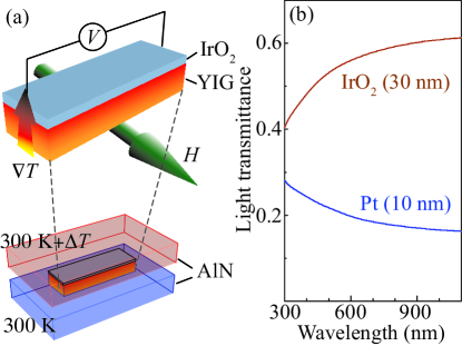
To investigate the SSE in the all-oxide system, a longitudinal configuration is employed in this work Uchida et al. (2010b, 2012). In Fig. 1(a), we show a schematic illustration of the experimental configuration and the sample structure of the IrO2/YIG bilayer film for measuring the longitudinal SSE (LSSE). The single-crystalline YIG film was grown on a 0.5-mm-thick (111) Gd3Ga5O12 (GGG) substrate by using a liquid phase epitaxy method. The thickness of the YIG film is about 4.5 m. A 30-nm-thick IrO2 film was then deposited on the YIG film by using an rf-sputtering method at room temperature. As shown in Fig. 1(b), the light transmittance of the 30-nm-thick IrO2 film is much higher than that of a conventional 10-nm-thick Pt film in the visible light range.
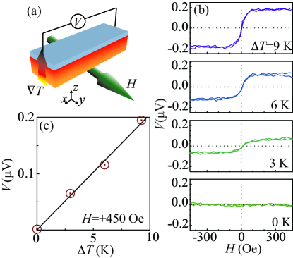
The LSSE measurements were performed by using an experimental setup similar to that described in Ref. Uchida et al. (2012). The IrO2/YIG sample with the size of mm2 was sandwiched between two AlN heat baths of which the temperatures were stabilized to and 300 K, where the temperature of the heat bath connected to the top of the IrO2 layer is higher than that connected to the bottom of the GGG substrate. The temperature difference was generated by using a Peltier thermoelectric module and detected by using thermocouples.
The temperature gradient across the IrO2/YIG interface induces a spin current in the IrO2 layer along the direction normal to the interface if the magnetic moments in YIG and conduction-carriers’ spins in IrO2 are coupled via the spin-mixing conductance. This spin current is converted into an electric field by the ISHE in the IrO2 layer along the direction determined by the following relation:
| (1) |
where , , , , and denote the spatial direction of the thermally generated spin current, spin-Hall angle, resistivity, spin-diffusion length, and thickness of the IrO2 film, respectively. is the real part of the spin-mixing conductance at the IrO2/YIG interface and M is the magnetization vector of the YIG film. In Eq. (1), we neglect the diffusion term of the spin current in the IrO2 film because () of our sample is much greater than of IrO2 ( Fujiwara et al. (2013)). The LSSE-induced in the IrO2 layer can be detected as an electric voltage signal with and respectively being the magnitude of and the effective sample length. To measure induced by the LSSE in the IrO2/YIG sample, two silver-paste electrodes were attached to the ends of the IrO2 layer with the interval of and the electric voltage difference between the two electrodes was measured with sweeping an external magnetic field at various values of .
Figure 2(b) shows the dependence of for various values of for the IrO2/YIG sample, measured when the magnetic field was applied along the direction. As increases, a clear voltage signal was found to appear in the IrO2 layer in response to the magnetization reversal of the YIG layer, while no signal was observed at K. The voltage signal is proportional to , and its linear fitting line shows that the thermopower in the IrO2/YIG sample is VK-1 [see Fig. 2(c)]. These results indicate that the voltage signal is attributed to the ISHE in the IrO2 layer generated by the LSSE in the YIG layer.
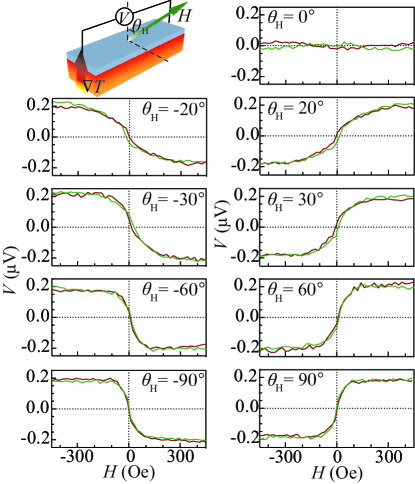
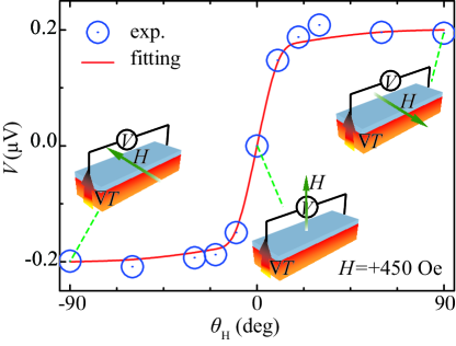
To further confirm the origin of the thermoelectric voltage in the IrO2/YIG sample, we measured with changing the angle of the external mangetic field. Figure 3 shows the dependence of for the IrO2/YIG sample at for various values of the out-of-plane field angle , where is defined as in the upper left panel of Fig. 3. When , finite signals appear and their magnitude and sign systematically change with . In contrast, no signal was observed when the magnetic field is perpendicular to the film surface: . The dependence of in the IrO2/YIG sample is well reproduced by Eq. (1) combined with static demagnetizing fields in the YIG film (see Fig. 4), consistent with the symmetry of the ISHE voltage induced by the LSSE.
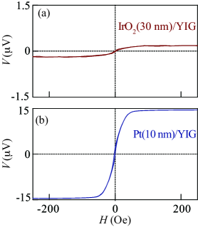
In Fig. 5, we show the comparison of the LSSE signals between the IrO2/YIG sample and conventional Pt/YIG sample. The Pt/YIG sample was prepared by sputtering a 10-nm-thick Pt film on YIG/GGG wafer, where the YIG films for the IrO2/YIG and Pt/YIG samples were grown at the same time. Both the samples have the same size ( mm2) and the LSSE measurements were carried out in the same condition at . The magnitude of the LSSE signal in the IrO2/YIG sample was found to be 68 times smaller than that in the Pt/YIG sample. Such a small LSSE signal in the IrO2/YIG sample is attributed not only to the thicker thickness of the IrO2 layer but also to the small spin-mixing conductance at the IrO2/YIG interface; by using Eq. (1) with Fujiwara et al. (2013) ( Rojas-Sánchez et al. (2014)) and cm (cm) for the IrO2 (Pt) film and at the Pt/YIG interface Qiu et al. (2013b), the spin mixing conductance at the IrO2/YIG interface is estimated to be . Therefore, improvement of the spin-mixing conductance at the conductive-oxide/magnetic-insulator interface is indispensable to realizing efficient all-oxide SSE devices, which may be achieved, for example, by improving crystalline structure of the interface by annealing treatmentQiu et al. (2013b), by modulating carrier density in the conductive oxide layer, and by inserting magnetic interlayers between the conductive-oxide and magnetic-insulator layersKikuchi et al. (2015).
In summary, we measured the longitudinal spin-Seebeck effect (LSSE) in the all-oxide IrO2/Y3Fe5O12 (YIG) bilayer film. The temperature-difference, magnetic-field, and field-angle dependences of the thermoelectric voltage in the IrO2/YIG sample are well consistent with the characteristics of the inverse spin-Hall effect in the IrO2 layer induced by the LSSE in the YIG layer. The LSSE voltage in the IrO2/YIG sample was observed to be much smaller than that in a conventional Pt/YIG sample, which may be attributed to the small spin-mixing conductance at the IrO2/YIG interface if the spin-Hall angle and spin-diffusion length of our IrO2 film are assumed to be comparable to those reported by previous studies. Although an all-oxide system is one of promising candidates for realizing low-cost, stable, and transparent LSSE thermospin devices, major improvement of the spin-mixing conductance at conductive-oxide/magnetic-insulator interfaces is necessary.
The authors thank A. Kirihara and M. Ishida for valuable discussions. This work was supported by PRESTO “Phase Interfaces for Highly Efficient Energy Utilization”, Strategic International Cooperative Program ASPIMATT from JST, Japan, Grant-in-Aid for Young Scientists (A) (25707029), Grant-in-Aid for Challenging Exploratory Research (26600067), Grant-in-Aid for Scientific Research (A) (24244051), Grant-in-Aid for Scientific Research on Innovative Areas “Nano Spin Conversion Science” (26103005) from MEXT, Japan, and NEC Corporation.
References
- Weiler et al. (2012) M. Weiler, M. Althammer, F. D. Czeschka, H. Huebl, M. S. Wagner, M. Opel, I. M. Imort, G. Reiss, A. Thomas, R. Gross, et al., Physical Review Letters 108, 106602 (2012).
- Uchida et al. (2008) K. Uchida, S. Takahashi, K. Harii, J. Ieda, W. Koshibae, K. Ando, S. Maekawa, and E. Saitoh, Nature 455, 778 (2008).
- Jaworski et al. (2010) C. M. Jaworski, J. Yang, S. Mack, D. D. Awschalom, J. P. Heremans, and R. C. Myers, Nature Materials 9, 898 (2010).
- Qu et al. (2013) D. Qu, S. Y. Huang, J. Hu, R. Wu, and C. L. Chien, Physical Review Letters 110, 067206 (2013).
- Agrawal et al. (2014) M. Agrawal, V. I. Vasyuchka, A. A. Serga, A. Kirihara, P. Pirro, T. Langner, M. B. Jungfleisch, a. V. Chumak, E. T. Papaioannou, and B. Hillebrands, Physical Review B 89, 224414 (2014).
- Rezende et al. (2014) S. M. Rezende, R. L. Rodríguez-Suárez, R. O. Cunha, A. R. Rodrigues, F. L. A. Machado, G. A. Fonseca Guerra, J. C. Lopez Ortiz, and A. Azevedo, Physical Review B 89, 014416 (2014).
- R. Ramos et al. (2013) R. Ramos, T. Kikkawa, K. Uchida, H. Adachi, I. Lucas, M. H. Aguirre, P. Algarabel, L. M. On, S. Maekawa, E. Saitoh, and M. R. Ibarra, Appl. Phys. Lett. 102, 072413 (2013).
- Meier et al. (2013) D. Meier, T. Kuschel, L. Shen, A. Gupta, T. Kikkawa, K. Uchida, E. Saitoh, J. M. Schmalhorst, and G. Reiss, Physical Review B 87, 054421 (2013).
- Uchida et al. (2010a) K. Uchida, J. Xiao, H. Adachi, J. Ohe, S. Takahashi, J. Ieda, T. Ota, Y. Kajiwara, H. Umezawa, H. Kawai, G. E. W. Bauer, S. Maekawa, and E. Saitoh, Nature Materials 9, 894 (2010a).
- Uchida et al. (2010b) K. Uchida, H. Adachi, T. Ota, H. Nakayama, S. Maekawa, and E. Saitoh, Applied Physics Letters 97, 172505 (2010b).
- Uchida et al. (2012) K. Uchida, T. Ota, H. Adachi, J. Xiao, T. Nonaka, Y. Kajiwara, G. E. W. Bauer, S. Maekawa, and E. Saitoh, Journal of Applied Physics 111, 103903 (2012).
- Kikkawa et al. (2013a) T. Kikkawa, K. Uchida, S. Daimon, Y. Shiomi, H. Adachi, Z. Qiu, D. Hou, X. F. Jin, S. Maekawa, and E. Saitoh, Physical Review B 88, 214403 (2013a).
- Kikkawa et al. (2013b) T. Kikkawa, K. Uchida, Y. Shiomi, Z. Qiu, D. Hou, D. Tian, H. Nakayama, X. F. Jin, and E. Saitoh, Physical Review Letters 110, 067207 (2013b).
- Kirihara et al. (2012) A. Kirihara, K. Uchida, Y. Kajiwara, M. Ishida, Y. Nakamura, T. Manako, E. Saitoh, and S. Yorozu, Nature Materials 11, 686 (2012).
- Roschewsky et al. (2014) N. Roschewsky, M. Schreier, A. Kamra, F. Schade, K. Ganzhorn, S. Meyer, H. Huebl, R. Gross, and S. T. B. Goennenwein, Applied Physics Letters 104, 202410 (2014).
- Uchida et al. (2014a) K. Uchida, M. Ishida, T. Kikkawa, A. Kirihara, T. Murakami, and E. Saitoh, Journal of Physics: Condensed matter 26, 343202 (2014a).
- Uchida et al. (2014b) K. Uchida, T. Kikkawa, A. Miura, J. Shiomi, and E. Saitoh, Phys. Rev. X 4, 041023 (2014b).
- Schreier et al. (2013) M. Schreier, N. Roschewsky, E. Dobler, S. Meyer, H. Huebl, R. Gross, and S. T. B. Goennenwein, Applied Physics Letters 103, 242404 (2013).
- Uchida et al. (2013) K. Uchida, T. Nonaka, T. Kikkawa, Y. Kajiwara, and E. Saitoh, Physical Review B 87, 104412 (2013).
- Bauer et al. (2012) G. E. W. Bauer, E. Saitoh, and B. J. van Wees, Nature Materials 11, 391 (2012).
- Geller and Gilleo (1957) S. Geller and M. A. Gilleo, Acta Crystallographica 10, 239 (1957).
- Cherepanov et al. (1993) V. Cherepanov, I. Kolokolov, and V. L’vov, Physics Reports 229, 81 (1993).
- Serga et al. (2010) A. A. Serga, A. V. Chumak, and B. Hillebrands, Journal of Physics D-Applied Physics 43, 264002 (2010).
- Qiu et al. (2013a) Z. Qiu, T. An, K. Uchida, D. Hou, Y. Shiomi, Y. Fujikawa, and E. Saitoh, Applied Physics Letters 103, 182404 (2013a).
- Qiu et al. (2012) Z. Qiu, Y. Kajiwara, K. Ando, Y. Fujikawa, K. Uchida, T. Tashiro, K. Harii, T. Yoshino, and E. Saitoh, Applied Physics Letters 100, 022402 (2012).
- Fujiwara et al. (2013) K. Fujiwara, Y. Fukuma, J. Matsuno, H. Idzuchi, Y. Niimi, Y. Otani, and H. Takagi, Nature Communications 4, 2893 (2013).
- Chalamala et al. (1999) B. R. Chalamala, Y. Wei, R. H. Reuss, S. Aggarwal, B. E. Gnade, R. Ramesh, J. M. Bernhard, E. D. Sosa, and D. E. Golden, Applied Physics Letters 74, 1394 (1999).
- Rojas-Sánchez et al. (2014) J. C. Rojas-Sánchez, N. Reyren, P. Laczkowski, W. Savero, J. P. Attané, C. Deranlot, M. Jamet, J. M. George, L. Vila, and H. Jaffrès, Physical Review Letters 112, 106602 (2014).
- Qiu et al. (2013b) Z. Qiu, K. Ando, K. Uchida, Y. Kajiwara, R. Takahashi, H. Nakayama, T. An, Y. Fujikawa, and E. Saitoh, Applied Physics Letters 103, 092404 (2013b).
- Kikuchi et al. (2015) D. Kikuchi, M. Ishida, K. Uchida, Z. Qiu, T. Murakami, and E. Saitoh, Appl. Phys. Lett. 106, 082401 (2015).