Capacitive coupling in hybrid Graphene/GaAs nanostructures
Abstract
Coupled hybrid nanostructures are demonstrated using the combination of lithographically patterned graphene on top of a two-dimensional electron gas (2DEG) buried in a GaAs/AlGaAs heterostructure. The graphene forms Schottky barriers at the surface of the heterostructure and therefore allows tuning the electronic density of the 2DEG. Conversely, the 2DEG potential can tune the graphene Fermi energy. Graphene-defined quantum point contacts in the 2DEG show half-plateaus of quantized conductance in finite bias spectroscopy and display the 0.7 anomaly for a large range of densities in the constriction, testifying to their good electronic properties. Finally, we demonstrate that the GaAs nanostructure can detect charges in the vicinity of the heterostructure’s surface. This confirms the strong coupling of the hybrid device: localized states in the graphene ribbon could in principle be probed by the underlying confined channel. The present hybrid graphene/GaAs nanostructures are promising for the investigation of strong interactions and coherent coupling between the two fundamentally different materials.
pacs:
81.05.ue, 73.22-b, 73.63.NmThe control of individual electrons in semiconductor nanostructures allows the investigation of electron-electron interactions at a basic level Kouwenhoven, Austing, and Tarucha (2001). Recently, it has become possible to study such phenomena in nanostructured graphene devices Güttinger et al. (2008). In such experiments, the coupling of neighboring quantum devices has to be understood and controlled in great detail. The combination of electronic devices made from different material systems, such as graphene on GaAs/AlGaAs heterostructures, offers unique opportunities for well-coupled electronic systems with strongly differing energy-momentum relations.
The technological challenge of combining graphene with a GaAs substrate proved to be laborious because of graphene’s invisibility on this substrate Calizo et al. (2007); Yu and Hilke (2009); Wurstbauer et al. (2010); Peters et al. (2011); Friedemann et al. (2009). Using visibility-enhancing GaAs/AlAs superlattices Friedemann et al. (2009), Woszczyna et al. could measure a state-of-the-art quantum resistance standard in a graphene Hall bar on insulating GaAs Woszczyna et al. (2011, 2012). Other works have bypassed the problem of the graphene invisibility by transferring chemical-vapor-deposited graphene on n-type GaAs chips to study the formation of Schottky barriers Tongay et al. (2012), and use them to fabricate Schottky-junction based solar cells Jie, Zheng, and Hao (2013).
Fewer works have studied the interaction of large-area graphene with a buried 2DEG in a GaAs/AlGaAs heterostructure. Tang et al. have demonstrated a micrometer-long graphene field-effect transistor gated by the 2DEG underneath Tang et al. (2012) and a highly tunable GaAs far infrared photodetector covered by a graphene top-gate Tang et al. (2014). The first Coulomb drag measurements in a micrometer-sized graphene/GaAs 2DEG bilayer system established the importance of Coulomb interactions between both charge carrier systems Gamucci et al. (2014).
In this work, we take the combination of the two materials one step further by forming GaAs nanostructures using Schottky barriers made of graphene. Our first sample is a GaAs quantum point contact (QPC) defined by graphene split-gates and our second sample consists of self-aligned and capacitively coupled graphene/GaAs constrictions. We present the fabrication, functionality, stability and electronic properties of these nanostructures. We finally demonstrate that the GaAs QPC acts as a detector for charges located close to the graphene gates.
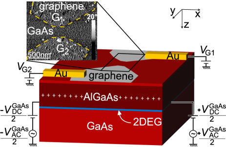
We fabricate hybrid nanostructures with the layer sequence schematically shown in Fig. 1. The GaAs/Al0.3Ga0.7As heterostructure comprises from top to bottom: a thick GaAs cap layer on the surface (), an thick AlGaAs layer including a Si doping layer of density cm-2 at below the surface, and a heterointerface at .
The 2DEG’s electron density, measured from the Hall effect, is with a mobility of , as measured using the Van der Pauw method without illumination at a temperature of . Graphene flakes are produced by mechanical exfoliation and their monolayer character is verified using Raman spectroscopy Ferrari et al. (2006); Graf et al. (2007). After optical lithography steps defining mesa, ohmic contacts and top-gate leads, the graphene flake is transferred onto the GaAs substrate following the method pioneered by Dean et al. Dean et al. (2010). Next, an electron beam lithography (EBL) step followed by a Ti/Au evaporation provides electrical contacts to the flake. The EBL resist is then removed with solvents and using atomic force microscope (AFM) mechanical cleaning Goossens et al. (2012). Finally, a second EBL exposure followed by an O2 plasma ashing step (W for s) defines the graphene device’s shape. The fabrication method and the choice of the etching technique are further explained in the supplemental material sup . Following these steps, we first fabricated two graphene split-gates, as shown in the inset of Fig. 1.
For this device, the differential conductance in the 2DEG is measured using a standard lock-in technique with a small AC excitation voltage between source (S) and drain (D) contacts at a frequency . All experiments are carried out in a 4He cryostat at a temperature of .
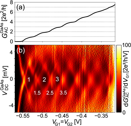
Applying a negative voltage to the two graphene split-gates G1 and G2 depletes the underlying 2DEG. The depletion voltage of graphene and of Ti/Au reference split-gates are the same within our experimental uncertainty (see Section I sup ). Hence, their contact potentials are similar. Moreover, we observe quantized conductance until pinch-off is reached, due to the formation of discrete modes in the 2DEG channel between the graphene gates. Figure 2(a) shows an example of the stepwise decrease in the GaAs differential conductance. As this is a two-point measurement, the resistance of the cables, bond wires, contacts, and mostly of the ohmic contacts to the 2DEG and of the 2DEG itself add to the resistance of the QPC. A serial resistance of has thus been subtracted from the data such that the fifth plateau resides at the expected conductance of . The observation of six conductance plateaus agrees well with the expectation based on the lithographic gap -nm between the graphene split-gates, which corresponds to a number of modes -.
In Fig. 2(b), we show the transconductance , with , as a function of split-gate voltage and DC bias voltage . The above-mentioned modes now draw a diamond pattern. Indeed, when increasing the split-gate voltage along V, each bright peak corresponds to another QPC subband falling below the Fermi level as the confinement potential is lowered. The dark regions correspond to the conductance plateaus occurring when the number of occupied modes is kept constant. As the bias voltage is increased, the bias window opens until it allows one additional subband to contribute to the conduction at the corners of the dark diamonds. Thus, the width in bias voltage of these diamonds gives a QPC subband spacing of meV.
Upon further increasing the bias voltage, additional dark regions are observed in Fig. 2(b). These diamonds are conductance plateaus at half-integer multiples of , often called half-plateaus. They occur when a subband-bottom resides between the source and drain chemical potentials Patel et al. (1991). Half-plateaus can vanish due to scattering events involving the electronic states available at higher bias. Hence, observing them testifies to the cleanliness and electrical stability of the device. Additionally, the quantized conductance plateaus and the half-plateaus have similar sizes, indicating that the confinement potential is close to harmonic Rössler et al. (2011). Thus, no observable degradation of transport properties results from the use of graphene top-gates or from the employed processing technology.
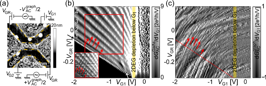
Having demonstrated the suitability of graphene as a top-gate, more involved graphene-GaAs hybrid nanostructures have been fabricated. Figure 3(a) shows an AFM topography image of our second device. It consists of a nm wide graphene nanoribbon (GR) with side-gates G1 and G2 on the same GaAs/AlGaAs heterostructure as for the first device. The differential conductance in the graphene ribbon is defined like for the 2DEG as using the same lock-in measurement technique as previously mentioned, with a source-drain (SD) voltage of for both graphene and 2DEG, and frequencies and .
The biased side-gates lead to the formation of a QPC in the 2DEG and the ribbon can be used to tune the density in its center. This is depicted in Fig. 3(b). The QPC transconductance is shown as a function of the gate voltage and the ribbon voltage . is kept constant at mV, such that the 2DEG underneath G2 is depleted. Figure 3(b) exhibits three regimes of conductance: for V (yellow band), a current can flow below G1 so electrons are not confined in a channel. For more negative , a QPC is formed and the conductance decreases stepwise. In this region, a decrease of reduces the electron density in the center of the channel, thus the plateaus and pinch-off positions occur at more positive . Finally, below the pinch-off voltage (black region), the QPC is completely depleted and no current can flow.
Below the first plateau at , a shoulder at is observed (black arrow, left of the graph). Its conductance value is stable for a large range of densities, therefore we attribute this shoulder to a quite pronounced 0.7 anomaly. Usually observed in clean 2DEGs with moderate bulk electron densities Rössler et al. (2011), the 0.7 anomaly has been found to be strongest at temperatures around Thomas et al. (1998); Kristensen et al. (1998). In agreement with other studies Thomas et al. (2000); Nuttinck et al. (2000), the anomaly shifts to lower conductance at low QPC electronic density, reaching for V. Interestingly, we find that this feature survives at lower densities in the channel than the first quantized plateau. This is in agreement with its general robustness with temperature and lateral shifting Thomas et al. (1998).
Additional features in the QPC conductance are observed at low , i.e. low density in the channel. A kink occurs on a line crossing the first three plateaus (white arrow). This is most probably the result of impurities creating local minima in the confinement potential of the channel. Electronic bound states form in these minima and transmission resonances appear Weis et al. (1992).
The current through the graphene ribbon top-gate can be measured simultaneously with the current in the QPC. Fig. 3(c) shows the graphene transconductance as a function of and recorded simultaneously with the data shown in Fig. 3(b). Smooth conductance fluctuations, commonly observed in graphene nanoribbons Han et al. (2007); Todd et al. (2008); Minke et al. (2012); Bischoff et al. (2014), are visible as a background. They have positive slopes because they occur at a constant values of the ribbon Fermi energy and because and have an opposite influence on them. When decreases, the ribbon Fermi energy increases, while a variation of is directly a variation of its Fermi energy.
Superimposed onto the broad conductance variations, fine lines (red arrows in the map) also have positive slopes, indicating tunnel-coupling to either the ribbon or G1 (see section IV sup for more details). However, they probably are not Coulomb resonances occurring in the graphene ribbon. Indeed, the transport gap in the ribbon cannot be reached within the accessible range of side-gates voltages. The graphene conductance in this map is above and increases on average with increasing (not shown), suggesting that the flake is -doped.
Instead, these fine lines can be explained by charge detection. Both QPCs and quantum dots have been shown to be sensitive detectors that can resolve a few percents of an electronic charge at a distance of a few hundred nanometers Field et al. (1993); Elzerman et al. (2003); Rössler et al. (2013). The strong conductance fluctuations in graphene nanoribbons make these structures sensitive detectors as well, even outside their transport gap. Variations of charge manifest themselves as kinks in the conductance of the detector, as seen in Fig. S4(c) sup . The narrow lines visible in Fig. 3(c) are thus attributed to charge traps detected by the graphene ribbon (see Section III sup for more details).
Similar measurements on a reference ribbon on SiO2 fabricated in the same way revealed that such resonances may come from residual carbon islands in the etched patterns left by the soft etching Simonet et al. (2015). The charge traps could also be impurities implanted during the etching process, but they cannot be located deep in the heterostructure since they should be tunnel-coupled to G1 or the ribbon.
These lines evolve differently in the three regimes mentioned for Fig. 3(b). For V (yellow band in Fig. 3(b) and (c), these fluctuations are barely influenced by because of the stronger capacitive coupling between G1 and the 2DEG underneath. Between the depletion voltage below G1 and the pinch-off voltage of the QPC (along the red dashed line in Fig. 3(c), the electronic density in the GaAs channel is decreased, so the influence of G1 on the charge traps and hence their slopes increase. Finally, the capacitive coupling between G1 and the traps is maximal when the QPC is completely depleted in the pinch-off region.
The same red arrows are drawn in Fig. 3(b), its inset and Fig. 3(c). Indicated by these arrows, the faint lines observed in Fig. 3(c) can also be faintly seen in Fig. 3(b) and with better visibility in the inset, where a directional derivative has been performed. Thus, the GaAs QPC also detects the same charge traps as seen in the graphene conductance. This means that the system is sufficiently well-coupled to allow the GaAs QPC to detect charges in the graphene plane. The next step could be the fabrication of a similar hybrid graphene-GaAs device with a graphene ribbon whose transport gap is accessible. The transfer of a boron-nitride flake before the graphene flake for instance would permit a more efficient etching process and a smaller doping of the final graphene ribbon. Spatial information on the ribbon’s localized charges in the transport gap could be gained using their detection by the GaAs QPC underneath.
In summary, we fabricated capacitively coupled graphene/GaAs nanostructures and characterized them by transport spectroscopy. Conductance quantization in the GaAs QPC could be observed. The observation of finite bias half-plateaus confirmed that this QPC exhibits high purity and charge stability. A second sample including a central graphene top-gate was used to observe the density dependence of the QPC conductance as the 2DEG is depleted. The presence of the 0.7 anomaly for a large range of densities was evidence of the quality of the device. Finally, we demonstrated mutual capacitive coupling between the graphene constriction and the GaAs QPC, including charge detection signals in the QPC conductance. Further high-quality hybrid nanostructures should allow probing localized states at graphene edges using the QPC defined in the GaAs 2DEG. Using shallower heterostructures, Coulomb drag in hybrid nanostructures or tunneling coupling between quasi-relativistic charge carriers in graphene with massive electrons in GaAs could be investigated.
Acknowledgements.
The authors would like to thank D. Bischoff and A. Kozikov for helpful discussions and R. Gorbachev for his advice on the graphene transfer technique. Support by the Marie Curie Initial Training Action (ITN) Q-NET 264034, the Marie Curie ITN S3 Nano and the ETH FIRST laboratory are gratefully acknowledged.References
- Kouwenhoven, Austing, and Tarucha (2001) L. P. Kouwenhoven, D. G. Austing, and S. Tarucha, Reports on Progress in Physics 64, 701 (2001).
- Güttinger et al. (2008) J. Güttinger, C. Stampfer, S. Hellmüller, F. Molitor, T. Ihn, and K. Ensslin, Applied Physics Letters 93, 212102 (2008).
- Calizo et al. (2007) I. Calizo, W. Bao, F. Miao, C. N. Lau, and A. A. Balandin, Applied Physics Letters 91, 201904 (2007).
- Yu and Hilke (2009) V. Yu and M. Hilke, Applied Physics Letters 95, 151904 (2009).
- Wurstbauer et al. (2010) U. Wurstbauer, C. Röling, U. Wurstbauer, W. Wegscheider, M. Vaupel, P. H. Thiesen, and D. Weiss, Applied Physics Letters 97, 231901 (2010).
- Peters et al. (2011) K. Peters, A. Tittel, N. Gayer, A. Graf, V. Paulava, U. Wurstbauer, and W. Hansen, Applied Physics Letters 99, 191912 (2011).
- Friedemann et al. (2009) M. Friedemann, K. Pierz, R. Stosch, and F. J. Ahlers, Applied Physics Letters 95, 102103 (2009).
- Woszczyna et al. (2011) M. Woszczyna, M. Friedemann, K. Pierz, T. Weimann, and F. J. Ahlers, Journal of Applied Physics 110, 043712 (2011).
- Woszczyna et al. (2012) M. Woszczyna, M. Friedemann, M. Götz, E. Pesel, K. Pierz, T. Weimann, and F. J. Ahlers, Applied Physics Letters 100, 164106 (2012).
- Tongay et al. (2012) S. Tongay, M. Lemaitre, X. Miao, B. Gila, B. R. Appleton, and A. F. Hebard, Physical Review X 2, 011002 (2012).
- Jie, Zheng, and Hao (2013) W. Jie, F. Zheng, and J. Hao, Applied Physics Letters 103, 233111 (2013).
- Tang et al. (2012) C.-C. Tang, M.-Y. Li, L. J. Li, C. C. Chi, and J.-C. Chen, Applied Physics Letters 101, 202104 (2012).
- Tang et al. (2014) C.-C. Tang, D. C. Ling, C. C. Chi, and J.-C. Chen, Applied Physics Letters 105, 181103 (2014).
- Gamucci et al. (2014) A. Gamucci, D. Spirito, M. Carrega, B. Karmakar, A. Lombardo, M. Bruna, L. N. Pfeiffer, K. W. West, A. C. Ferrari, M. Polini, and V. Pellegrini, Nature Communications 5 (2014), 10.1038/ncomms6824.
- Ferrari et al. (2006) A. C. Ferrari, J. C. Meyer, V. Scardaci, C. Casiraghi, M. Lazzeri, F. Mauri, S. Piscanec, D. Jiang, K. S. Novoselov, S. Roth, and A. K. Geim, Physical Review Letters 97, 187401 (2006).
- Graf et al. (2007) D. Graf, F. Molitor, K. Ensslin, C. Stampfer, A. Jungen, C. Hierold, and L. Wirtz, Nano Letters 7, 238 (2007).
- Dean et al. (2010) C. R. Dean, A. F. Young, I. Meric, C. Lee, L. Wang, S. Sorgenfrei, K. Watanabe, T. Taniguchi, P. Kim, K. L. Shepard, and J. Hone, Nature Nanotechnology 5, 722 (2010).
- Goossens et al. (2012) A. M. Goossens, V. E. Calado, A. Barreiro, K. Watanabe, T. Taniguchi, and L. M. K. Vandersypen, Applied Physics Letters 100, 073110 (2012).
- (19) See supplemental material at [URL] for more details on the Ti/Au reference split-gates, on the choice in processing techniques, on charge detection in our system and on our argument for tunnel-coupled charge traps.
- Patel et al. (1991) N. K. Patel, J. T. Nicholls, L. Martin-Moreno, M. Pepper, J. E. F. Frost, D. A. Ritchie, and G. A. C. Jones, Physical Review B 44, 13549 (1991).
- Rössler et al. (2011) C. Rössler, S. Baer, E. d. Wiljes, P.-L. Ardelt, T. Ihn, K. Ensslin, C. Reichl, and W. Wegscheider, New Journal of Physics 13, 113006 (2011).
- Thomas et al. (1998) K. J. Thomas, J. T. Nicholls, N. J. Appleyard, M. Y. Simmons, M. Pepper, D. R. Mace, W. R. Tribe, and D. A. Ritchie, Physical Review B 58, 4846 (1998).
- Kristensen et al. (1998) A. Kristensen, P. E. Lindelof, J. Bo Jensen, M. Zaffalon, J. Hollingbery, S. W. Pedersen, J. Nygård, H. Bruus, S. M. Reimann, C. B. Sørensen, M. Michel, and A. Forchel, Physica B: Condensed Matter 249–251, 180 (1998).
- Thomas et al. (2000) K. J. Thomas, J. T. Nicholls, M. Pepper, W. R. Tribe, M. Y. Simmons, and D. A. Ritchie, Physical Review B 61, R13365 (2000).
- Nuttinck et al. (2000) S. Nuttinck, K. Hashimoto, S. Miyashita, T. Saku, Y. Yamamoto, and Y. Hirayama, Japanese Journal of Applied Physics 39, L655 (2000).
- Weis et al. (1992) J. Weis, R. J. Haug, K. v. Klitzing, and K. Ploog, Physical Review B 46, 12837 (1992).
- Han et al. (2007) M. Y. Han, B. Özyilmaz, Y. Zhang, and P. Kim, Physical Review Letters 98, 206805 (2007).
- Todd et al. (2008) K. Todd, H.-T. Chou, S. Amasha, and D. Goldhaber-Gordon, Nano Letters 9, 416 (2008).
- Minke et al. (2012) S. Minke, J. Bundesmann, D. Weiss, and J. Eroms, Physical Review B 86, 155403 (2012).
- Bischoff et al. (2014) D. Bischoff, F. Libisch, J. Burgdörfer, T. Ihn, and K. Ensslin, Physical Review B 90, 115405 (2014).
- Field et al. (1993) M. Field, C. G. Smith, M. Pepper, D. A. Ritchie, J. E. F. Frost, G. A. C. Jones, and D. G. Hasko, Physical Review Letters 70, 1311 (1993).
- Elzerman et al. (2003) J. M. Elzerman, R. Hanson, J. S. Greidanus, L. H. Willems van Beveren, S. De Franceschi, L. M. K. Vandersypen, S. Tarucha, and L. P. Kouwenhoven, Physical Review B 67, 161308 (2003).
- Rössler et al. (2013) C. Rössler, T. Krähenmann, S. Baer, T. Ihn, K. Ensslin, C. Reichl, and W. Wegscheider, New Journal of Physics 15, 033011 (2013).
- Simonet et al. (2015) P. Simonet, D. Bischoff, A. Moser, T. Ihn, and K. Ensslin, arXiv:1503.01921 [cond-mat] (2015), arXiv: 1503.01921.