Quantum spin Hall phase in multilayer graphene
Abstract
The so called quantum spin Hall phase is a topologically non trivial insulating phase that is predicted to appear in graphene and graphene-like systems. In this work we address the question of whether this topological property persists in multilayered systems. We consider two situations: purely multilayer graphene and heterostructures where graphene is encapsulated by trivial insulators with a strong spin-orbit coupling. We use a four orbital tight-binding model that includes the full atomic spin-orbit coupling and we calculate the topological invariant of the bulk states as well as the edge states of semi-infinite crystals with armchair termination. For homogeneous multilayers we find that even when the spin-orbit interaction opens a gap for all the possible stackings, only those with odd number of layers host gapless edge states while those with even number of layers are trivial insulators. For the heterostructures where graphene is encapsulated by trivial insulators, it turns out that the interlayer coupling is able to induce a topological gap whose size is controlled by the spin-orbit coupling of the encapsulating materials, indicating that the quantum spin Hall phase can be induced by proximity to trivial insulators.
pacs:
73.22.Pr, 73.43.CdI Introduction
In their seminal papers,Kane2005 Kane and Mele established the existence of two fundamentally different types of band insulators with time reversal symmetry in two dimensions, dubbed as trivial and topological. Remarkably, it was predicted that monolayer graphene would be topological, giving rise to protected chiral gapless edge states. Importantly, this opened a new venue in condensed matter physics, the quest of searching and designing topological states in two dimensional systems.
The nature of the topological state in graphene comes from the intrinsic spin-orbit coupling (SOC). In particular, SOC will open gaps of opposite signs at the two Dirac points, in contrast with the trivial gap that a staggered potential opens in the honeycomb lattice, with the same sign at the two valleys. This twisting of the wave functions in the reciprocal space leads to the appearance of in-gap states at the boundaries of the material. Subsequent workMin2006 ; Yao2007 ; Gmitra2009 found that the size of the SOC gap in graphene was very small, and the attention shifted to other systems, such as CdTe/HgTe quantum wellsBernevig2006a in which the quantum spin Hall (QSH) phase was foundKonig2007 as well as to bulk systems, for which the notion of topologically non-trivial insulators was extended. Experimental evidence for quantum spin Hall phase has also been found in other systems, such as Bi(111) atomically thin layersSabater2013 ; Drozdov2014 , and InSb/GaSb quantum wellsZhang2014 ; Knez2011 .
Multilayers of two dimensional materials are also potential candidates to sustain topological states. In particular, their appealing comes from the the tunability of stacking a different number of layers, or even different materials. In the present work we will focus on the study of a particular type of multilayer systems, whose basic building blocks are graphene-like systems. We will study mainly two families of multilayers. First we consider multilayered systems formed by graphene-like insulators using the SOC as a free parameter, so the main concepts should be suitable for systems such as graphene, SiliceneVogt2012 ; Fleurence2012 ; Xu2012 , GermaneneHoussa2010 or StaneneXu2013 (in fact our methods make it easy to extended this kind of analysis to the case of BismuthMurakami2006 ; Sabater2013 ; Drozdov2014 , and metal-organic frameworksZhou2014 ; Davila2014 ; Lalmi2010 ; Liu2011 ; Tang2014 ; Petit2009 ; Rodenas2014 ). Second, stacks formed by a layer of graphene encapsulated by some trivial insulator with a strong SOC.
From a practical point of view, several reasons motivate this work. First, there is a generic interest in the possibility of engineering the electronic properties of two dimensional crystals, such as graphene, h-BN and transition metal dichalcogenides, by combining them into multilayersGiovannetti2007 ; Kosmider2013 ; Geim2013 . Stacking monolayers of the same type is also a very interesting and widely studied possibility.
Our second motivation is to study the behavior of the topological gap as we increase the number of layers in the system. In the case of graphene, it is well known that key electronic properties, such as the pattern of Landau levels and the density of states at the Dirac point are drastically modified for bilayerMcCann2013 and trilayer graphene.McCann2006 ; Konschuh2011a ; Zhang2010 ; Coletti2013 ; Min2008 . Recent experimental work shows that some sort of magnetic order can occur, even at in bilayerFreitag2012 ; Velasco2014 , trilayerLee2014 and even tetralayersGrushina2015 . These last trivial symmetry breaking states, will compete with the potential topological states studied in our work.
A third motivation comes from recent experimentsAvsar2014 that report a very large enhancement of the spin Hall effect for graphene deposited on top of WS2, as trivial semiconductor with a quite large SOC. This inspires the calculation for graphene placed between two insulators with a trivial band gap, large SOC and broken inversion symmetry, to mimic the properties of WS2 and related transition metal dichalcogenides.
Furthermore, we have also a formal motivation. It is not obvious a priori that the original second-neighbor hopping Hamiltonian Kane2005 can be applied to multilayer grapheneCortijo2010 . In monolayer graphene the orbitals are strictly decoupled from the , , orbitals, due to mirror symmetry with respect to the plane. In the monolayer, SOC mixes with and orbitals of opposite spin and, when treated perturbatively, leads to an effective HamiltonianKane2005 with a spin-dependent effective second-neighbor hopping between orbitals that conserves . In multilayer graphene this is no longer true, since electrons in a orbital in one layer can hop to the orbital of atoms in the next layer. When SOC is added to the model, we expect that this mixing naturally leads to spin-mixing terms in the Hamiltonian, which is indeed the case.Guinea2010 The presence of this spin-flip channel interaction cast a doubt on the validity of the spin-conserving Kane-Mele model for multilayersPrada2011 ; Qiao2011 and motivates our choice of the standardKonschuh2010 ; Min2006 ; Kormanyos2013 ; McCann2010 ; Fratini2013 four orbital tight-binding calculations.
The rest of this work is organized as follows. In section II we briefly review the tight-binding model and the procedures to determine the existence of a QSH phase applied to the homogeneous case, studying the relation between interlayer coupling and the topological properties of the system. In section III the same methodology is applied to the case of a heterogeneous structure, graphene encapsulated by a trivial insulator, finding that topological properties can be induced even by trivial neighboring layers. Finally, in section IV we summarize our findings.
II Homogeneous multilayers
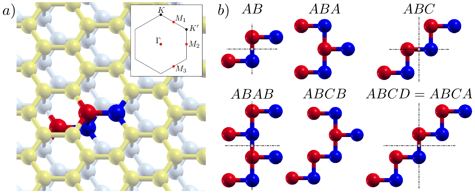
Monolayer graphene consists of a triangular lattice with two atoms per unit cell that leads, in the reciprocal space, to a hexagonal Brillouin zone that hosts Dirac cones in its corners. When layers are considered the crystalline structure remains the same, only there will be atoms per unit cell. We shall only use the so called Bernal stacking, shown in Fig. (1), which is the ground state configuration, according to both DFT calculations and experimental evidenceNorimatsu2010 ; Charlier1994 ; Charlier1994a . In Bernal stacked materials an atom from the sublattice () sits on top of an atom belonging to the other sublattice (). For there is only one way to achieve this, but for there are different possible stacking orders. In figure 1 we show the different possibilities for , with a self-evident notation.
II.1 The Model
We describe the multilayers with the following tight-binding Hamiltonian:
| (1) |
where and account for the intralayer and interlayer hoppings, respectively, and the last term is the intra-atomic SOC. Our tight-binding model is based on four atomic orbitals, , , and . Both the intralayer and interlayer hoppings are described within the Slater-Koster formalismSlater1954 . The intralayer hopping parameters are taken from Ref Gosalbez-Martinez2011 . In order to study the effect of interlayer coupling, the interlayer terms are scaled by a dimensionless parameter . When , the ratio between interlayer and intralayer in graphene is taken asKatsnelson2012 0.13. Unless otherwise stated, in all our calculations we have . Within this model, the dimension of the Hilbert space for the minimal unit cell of the crystal with layers is (4 orbitals per atom, 2 atoms per layer, plus the two possible spin orientations).
Without SOC, this model reproduces the very well known band structure of graphene () and multilayer graphene , that portraits these systems as zero-gap semiconductors. Within this model, SOC is known to open a gap in the monolayerMin2006 as well as in the bilayer Konschuh2012 ; Guinea2010 ; Cortijo2010 . In the case of the monolayer graphene the gap is known to be topological. Within this model, the computed value of the gap eV when we take a realistic value of the atomic spin orbit coupling, meV. This gap is much smaller than the ones obtained with accurate density functional theory (DFT) calculations, in the range of 30eVKonschuh2011a . The reason for the discrepancy turns out to be that the mayor contribution to the SOC gap at the Dirac point comes from the coupling to the higher energy bandsKonschuh2011a ; Konschuh2012 . The later is a simple consequence of the fact that SOC opens a gap in second order in the coupling in the Dirac points when projected over the band. In comparison, SOC acts as first order when considering channels involving the band. Nevertheless, interlayer hopping may open a first order spin flipping channel in the manifold, becoming of the same order as the intrinsic spin conserving -level contribution. These last processes would be the ones missing in the multilayer Kane-Mele model, and should be added for completeness. In our case, for the sake of simplicity, we will focus on the spin flipping channel, and use a four orbital tight-binding model considering as a free parameter.
Future work shall focus on the effect of the d-levels in multilayer graphene, which will not be addressed here.
The effect of SOC on the band structure of the multilayers can be summarized in the following points:
-
1.
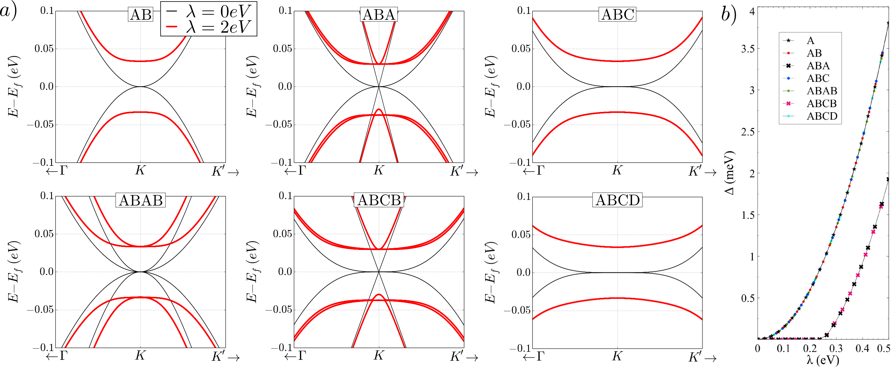
SOC opens up a gap for all the stacked layers considered, reproducing the existing resultsGuinea2010 for the case of . Notice that in the case of and stackings, the system remains gapless until a critical value of . This peculiarity is related to the non uniform evolution of the SO splitting of the linear and non-linear bands as shown in figure 2.
-
2.
The scaling of the gap with is very similar for monolayer and multilayers as it is shown in Figure 2. Therefore, it is expected that within this model, the gap opened by the intrinsic SOC might be as small in multilayers as in monolayers.
-
3.
The magnitude of the band-gap is insensitive to the interlayer coupling. This result is somewhat surprising, since together with atomic SOC the interlayer coupling opens a spin-flip channel, otherwise missing in the monolayer case. In particular, switching on the interlayer coupling does not close the SOC gap of the monolayer as shown in Figure 2. As a consequence, the ground state of two decoupled () monolayers can be adiabatically connected to the ground state of the bilayer ().
The last observation leads to the following result: odd stacked graphene will be quantum spin Hall Insulators, whereas even will not. More precisely, for a system of decoupled monolayers the invariant is:
| (2) |
Since the gap opened by remains unaffected when switching on the interlayer coupling , the value of for graphene-like multilayers is also given by equation (2). In the following we verify equation (2) using two different strategies. In the case of inversion symmetric structures, we compute the invariant. In all cases, we compute the edge states and check whether they fill the gap, or else. Independently on how the topological character is obtained, eq. (2) holds in all the cases.
II.2 Calculation of the invariant.
Using the method developed by Fu and Kane in 2007Fu2007 for systems with inversion symmetry it is possible to determine easily its topological character (the invariant) by calculating the parity of the occupied Bloch wave functions at the time reversal invariant momenta (TRIMs).
| (3) |
where is the parity eigenvalue of the occupied state at the TRIM . Using this method the topological character of a system will be determined just by the quantity , resulting that means trivial topology and means non trivial topology. The calculation for the systems with inversion symmetry yields the following results:
| A | AB | ABC | ABAB | ABCD | |
|---|---|---|---|---|---|
This guarantees that and crystals are topological but the bilayers and tetralayers (with inversion symmetry) are not. This method cannot be applied to systems without inversion symmetry, which are addressed in the next section using a different approach.
II.3 Edge states
To confirm equation (2) even for systems without inversion symmetry we look for the presence of gapless edge states. We consider armchair-terminated semi-infinite crystals. Using translation invariance along the direction parallel to the edge, we block-diagonalize the Hamiltonian of the semi-infinite 2D crystal in terms of a collection of dependent semi-infinite 1D Hamiltonians, as indicated in figure (3). The 1D Hamiltonian describes unit cells with atoms, where stands for the number of graphene layers. The intra-cell terms are denoted by and the inter-cell hoppings by .
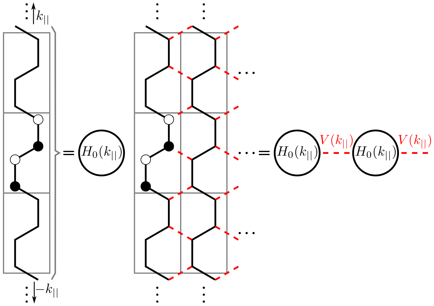
The surface Green function of this block tridiagonal semi-infinite matrix can be written as:
| (4) |
where is a self-energy that accounts for the coupling to the semi-infinite crystal, is the self-energy due to its interaction with the atoms included to get rid of the dangling bonds and a small analytic continuation.
The self-energy can be calculated employing a recursive Green’s function method that leads to the following coupled equations
| (5) |
The is calculated just as an additional iteration to the self-consistent calculation with the appropriate value for the hoppings .
For a given we compute the density of states using
| (6) |
Using a similar approach we can also obtain the bulk density of states calculating the bulk Green function by recursion.
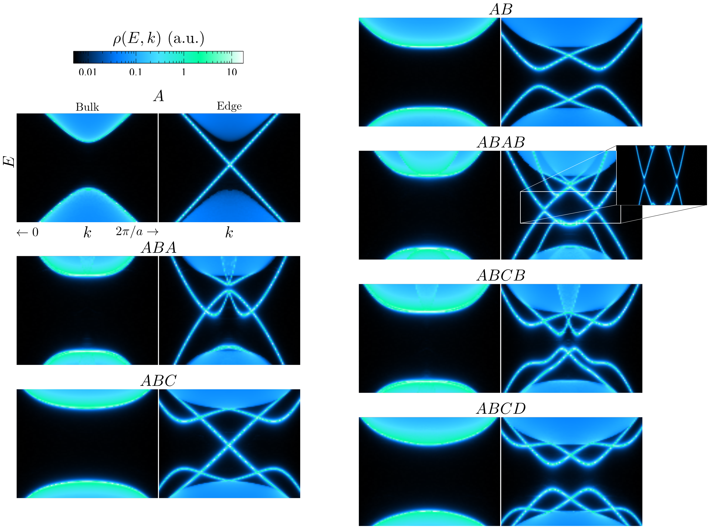
In figure 4 we show the density of states for both bulk and edge for all the stackings as a contour plot in the plane. For each stacking the left panel shows the bulk density of states, which are gaped for all the stackings and the right panel shows the edge states. The calculations are done for a rather large value of eV. The first thing to notice is that, for such large values of , all the structures have edge states. However, only in the case of odd , shown in the left column, the in-gap states are gapless. This is a necessary condition in order to have a QSHI. In contrast, all systems with even have edge states with a gap. Thereby, they are definitely not in the QSH phase, validating equation (2). Therefore, we conclude that odd graphene stacks are QSHI and even are trivial insulators. In all cases, the gap opened by SOC is quite small.
III Heterogeneous multilayers
In the previous section we have seen that for homogeneous multilayers the gap opened by SOC has the same magnitude than for the monolayer. Thereby, homogeneous multilayers of graphene would not improve the prospects for observation of the QSH phase compared to the monolayer. We thus explore the case of a heterogeneous multilayer. This is motivated in part by recent experiments Avsar2014 that seem to indicate an enhancement of the SOC interaction in graphene due to proximity to WS2, a trivial semiconductor with quite large SOC and no inversion symmetry. There has also been plenty of work studying the enhancement of SOC interaction in graphene due to proximity to heavy metalsZhang2014a . However, it would be much more interesting if graphene could be driven into a QSH phase by proximity to an insulator, so that the only conducting channels would be only at the edges of graphene.
Density functional calculations showKaloni2014 that a topological band-gap opens in graphene on top of both WS2 and WSe2, two widely studied two dimensional transition metal dichalcogenides (TMD). The magnitude of this gap is in the range of a few meV, i.e., two or three orders of magnitude larger than the intrinsic SOC gap.
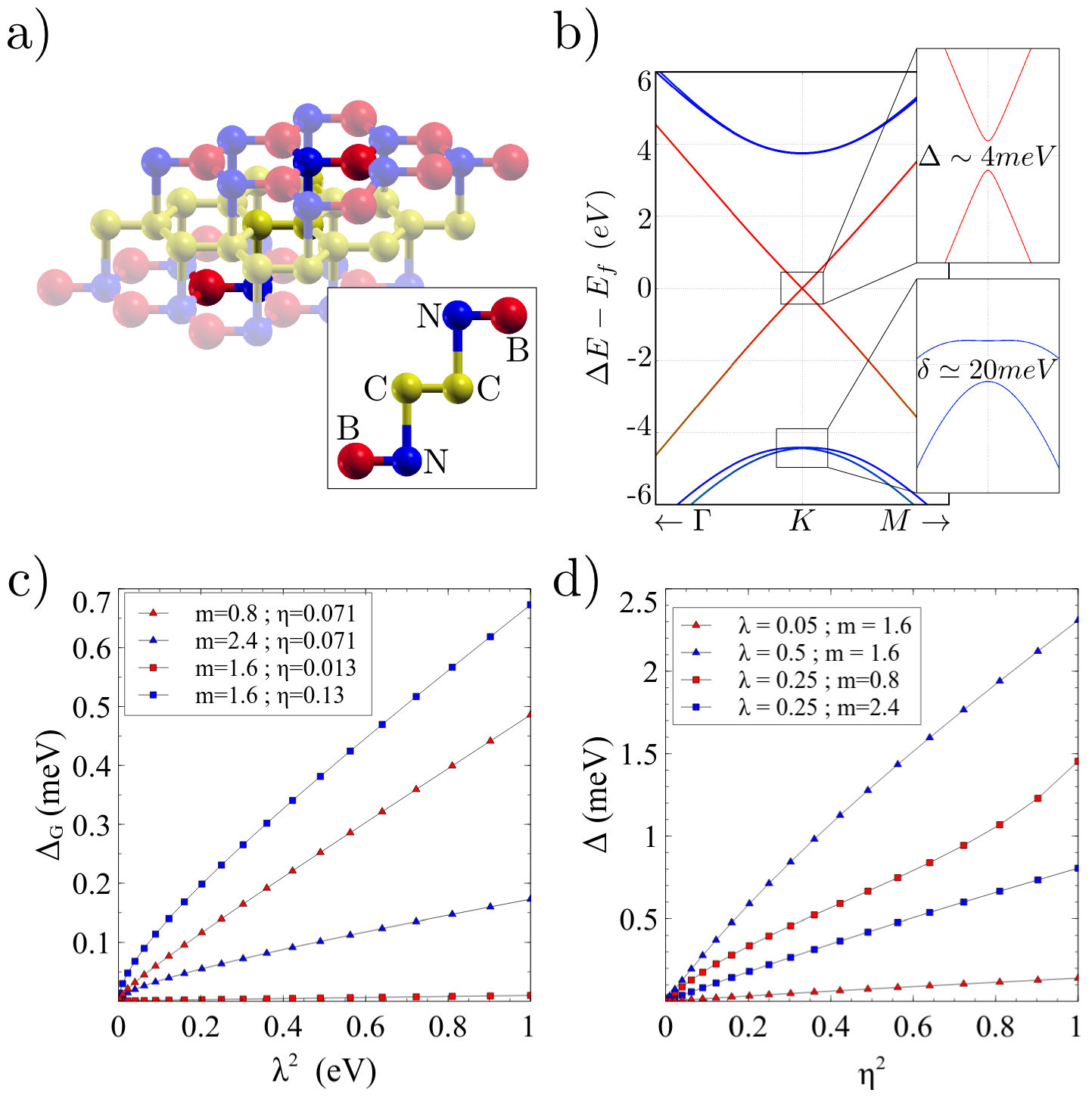
Here we propose a toy model to understand the opening of a non-trivial gap due to proximity to a trivial insulator with strong spin orbit coupling. For that matter, we take graphene encapsulated between two monolayers of a trivial semiconductor with strong SOC and broken inversion symmetry. Specifically, the structure of these adjacent monolayers is that of a BN-like crystal (see figure 5(a)). The choice of the stacking is such that, globally, the structure has inversion symmetry. Otherwise, a trivial band gap would be opened by proximityGiovannetti2007 .
The BN-like crystal is described with the same interatomic Slater-Koster parameters than graphene, but very different on-site parameters. In particular we assume a large SOC and a staggered potential that breaks inversion symmetry of the top and bottom layers. Since we are interested in the proximity effect, we turn off the atomic SOC of the graphene layer. As in the case of the homogeneous multilayers, the interlayer coupling is characterized by the dimensionless parameter . In this case we impose zero SOC for the graphene layer, in order to study the proximity effect. For the bands of this system would be the superposition of those of the top and bottom insulators, with gap , and the bands of graphene, whose Dirac cones would lie inside the gap. Broadly speaking, this picture remains the same as the interlayer coupling is turned on. Interestingly, a non-trivial gap opens in the Dirac cones only when and . We have verified that this gap satisfies the scaling
| (7) |
in the limit of small , and . This results implies that graphene can borrow SOC from a neighbor trivial insulator layer via interlayer coupling. Using the method of the TRIM we have verified that this insulator has , and is therefore topologically non-trivial.
The magnitude of the proximity effect away from the weak coupling limit of eq. (7) is shown in figures 5. We study the dependence of the proximity gap as a function of both the SOC and the interlayer coupling for two values of the encapsulating layer staggered potential . It is apparent that, taking (a trivial gap ) and eV, values in line with those of 2D TMD, the proximity gap is in the order of 1meV, similar to the DFT results. Therefore, our model provides a reasonable justification of the DFT computations, which are certainly more complete.
Our toy model does not capture some probably important features of real heterogeneous multilayers. For instance, the interlayer interaction could break inversion symmetry which is expected to open a trivial gap. In addition, the geometry of our encapsulating layers was chosen to minimize the size of the unit cell, rather than to describe a real material. In general, the coupling of graphene to other 2D crystals will imply a new length scale, given by the size of the new unit cell. In this setup, the inversion symmetry breaking could average out.
IV Conclusions
We have studied the quantum spin Hall phase in multilayer graphene and in graphene encapsulated by a trivial semiconductor. In the case of multilayer graphene we find that only the stacks with an odd number of layers are quantum spin Hall insulators. However, the size of the gap is the same than for a monolayer, and thereby, most likely too small to be detected experimentally. In contrast, we propose a toy model for graphene encapsulated between two semiconducting layers with strong SOC and a trivial gap. Our model shows that a non-trivial gap can be opened in graphene whose magnitude is controlled by the atomic spin orbit coupling of the adjacent layers. Our model provides a qualitative understanding of recent DFT calculationsZhang2014a as well as recent experimental workAvsar2014 and shows a promising route to observe the quantum spin Hall phase in graphene.
V Acknowledgments
JFR acknowledges financial supported by MEC- Spain (FIS2010-21883-C02-01) and Generalitat Valenciana (ACOMP/2010/070), Prometeo. This work has been financially supported in part by FEDER funds. We acknowledge financial support by Marie-Curie-ITN 607904-SPINOGRAPH. J. L. Lado and N. Garcia thank the hospitality of the Departamento de Fisica Aplicada at the Universidad de Alicante.
References
- (1) C. L. Kane and E. J. Mele, Phys. Rev. Lett. 95, 226801 (2005).
- (2) H. Min, J. E. Hill, N. A. Sinitsyn, B. R. Sahu, L. Kleinman, and A. H. MacDonald, Phys. Rev. B 74, 165310 (2006).
- (3) Y. Yao, F. Ye, X. Qi, S. Zhang, and Z. Fang, Phys. Rev. B 75, 041401(R) (2007).
- (4) M. Gmitra, S. Konschuh, C. Ertler, C. Ambrosch-Draxl, and J. Fabian, Phys. Rev. B 80, 235431 (2009).
- (5) B. Andrei Bernevig, T. L. Hughes, S. Zhang, Science 15, 314, 5806 (2006).
- (6) M. König, S. Wiedmann, C. Brüne, A. Roth, H. Buhmann, L. W. Molenkamp, X. Qi, S. Zhang, Science 2, 318, 5851. 766-770 (2007).
- (7) C. Sabater, D. Gosálbez-Martínez, J. Fernández-Rossier, J. G. Rodrigo, C. Untiedt, and J. J. Palacios, Phys. Rev. Lett. 110, 176802 (2013).
- (8) I. K. Drozdov, A. Alexandradinata, S. Jeon, S. Nadj-Perge, H. Ji, R. J. Cava, B. A. Bernevig and A. Yazdani, Nature Physics 10, 664–669 (2014).
- (9) H. Zhang, Y. Xu, J., K. Chang, and S. Zhang, Phys. Rev. Lett. 112, 216803 (2014).
- (10) I. Knez, R. Du, Frontiers of Physics 7, 2, 200-207 (2011).
- (11) P. Vogt, P. De Padova, C. Quaresima, J. Avila, E. Frantzeskakis, M. C. Asensio, A. Resta, B. Ealet, and G. Le Lay, Phys. Rev. Lett. 108, 155501 (2012).
- (12) A. Fleurence, R. Friedlein, T. Ozaki, H. Kawai, Y. Wang, and Y. Yamada-Takamura, Phys. Rev. Lett. 108, 245501 (2012).
- (13) C. Xu, G. Luo, Q. Liu, J. Zheng, Z. Zhang, S. Nagase, Z. Gao, and J. Lu, Nanoscale 4, 3111 (2012).
- (14) M. Houssa, G. Pourtois, V. V. Afanas’ev, and A. Stesmans, Appl. Phys. Lett. 96, 1 (2010).
- (15) L. Xu, Y. Zhou, and C.-D. Gong, J. Phys. Condens. Matter 25, 335503 (2013).
- (16) S. Murakami, Phys. Rev. Lett. 97, 1 (2006).
- (17) Jin-Jian Zhou, Wanxiang Feng, Gui-Bin Liu and Yugui Yao New J. Phys. 17 015004 (2015).
- (18) M. E. Davila, L. Xian, S. Cahangirov, A. Rubio, and G. Le Lay, New J. Phys. 16, 095002 (2014).
- (19) B. Lalmi, H. Oughaddou, H. Enriquez, A. Kara, S. Vizzini, B. Ealet, and B. Aufray, Appl. Phys. Lett. 97, 223109 (2010).
- (20) C. Liu, H. Jiang, and Y. Yao, Phys. Rev. B 84, 195430 (2011).
- (21) P. Tang, P. Chen, W. Cao, H. Huang, S. Cahangirov, L. Xian, Y. Xu, S. Zhang, W. Duan, and A. Rubio, Phys. Rev. B 90, 121408 (2014).
- (22) C. Petit and T. J. Bandosz, Adv. Mater. 21, 46, 4753–4757, (2009).
- (23) T. Rodenas, I. Luz, G. Prieto, B. Seoane, H. Miro, A. Corma, F. Kapteijn, F. X. Llabres i Xamena and J. Gascon. Nature Materials 14 (2015)
- (24) G. Giovannetti, P. A. Khomyakov, G. Brocks, P. J. Kelly, and J. Van Den Brink, Phys. Rev. B 76, 2 (2007).
- (25) K. Kosmider and J. Fernández-Rossier, Phys. Rev. B 87, 2 (2013)
- (26) A. K. Geim and I. V. Grigorieva, Nature 499, 419 (2013).
- (27) E. McCann and M Koshino, Rep. Prog. Phys. 76 056503 (2013).
- (28) E. McCann and V. Falko, Phys. Rev. Lett. 96, 086805 (2006).
- (29) S. Konschuh, M. Gmitra, and J. Fabian, Phys. Rev. B 82, 245412 (2010).
- (30) F. Zhang, B. Sahu, H. Min, and A. H. MacDonald, Phys. Rev. B 82, 035409 (2010).
- (31) C. Coletti, S. Forti, A. Principi, K. V. Emtsev, A. A. Zakharov, K. M. Daniels, B. K. Daas, M. V. S. Chandrashekhar, T. Ouisse, D. Chaussende, A. H. MacDonald, M. Polini, and U. Starke, Phys. Rev. B 88, 155439 (2013).
- (32) H. Min and A. H. MacDonald, Prog. Theor. Phys. Suppl. 176, 227 (2008).
- (33) F. Freitag, J. Trbovic, M. Weiss, and C. Schönenberger Phys. Rev. Lett. 108, 076602 (2012).
- (34) J. Velasco Jr, Y. Lee, F. Zhang, K. Myhro, D. Tran, M. Deo, D. Smirnov, A. H. MacDonald and C. N. Lau, Nature Communications 5, 4550 (2014).
- (35) Y. Lee, D. Tran, K. Myhro, J. Velasco, N. Gillgren, C. N. Lau, Y. Barlas, J. M. Poumirol, D. Smirnov and F. Guinea, Nature Communications 5, 5656 (2014).
- (36) A. L. Grushina, D.-K. Ki, M. Koshino, A. A. L. Nicolet, C. Faugeras, E. McCann, M. Potemski, and A. F. Morpurgo, Nature Communications 6, 6419 (2015).
- (37) A. Avsar, J. Y. Tan, T. Taychatanapat, J. Balakrishnan, G. K. W. Koon, Y. Yeo, J. Lahiri, A. Carvalho, A. S. Rodin, E. C. T. O’Farrell, G. Eda, A. H. Castro Neto, and B. Ozyilmaz, Nature communications 5, 4875 (2014).
- (38) A. Cortijo, A. G. Grushin, and M. A. H. Vozmediano, Phys. Rev. B 82, 195438 (2010).
- (39) F. Guinea, New J. Phys. 12, 083063 (2010).
- (40) E. Prada, P. San-Jose, L. Brey, and H. Fertig, Solid State Commun. 151, 1075 (2011).
- (41) Z. Qiao, W.-K. Tse, H. Jiang, Y. Yao, and Q. Niu, Phys. Rev. Lett. 107, 256801 (2011).
- (42) S. Konschuh, M. Gmitra, and J. Fabian, Phys. Rev. B 82, 245412 (2010).
- (43) A. Kormányos and G. Burkard, Phys. Rev. B 87, 045419 (2013).
- (44) E. McCann and M. Koshino, Phys. Rev. B 81, 4 (2010).
- (45) S. Fratini, D. Gosalbez-Martinez, P. M. Cámara, and J. Fernández-Rossier, Phys. Rev. B 88, 115426 (2013).
- (46) W. Norimatsu and M. Kusunoki, Phys. Rev. B 81, 161410 (2010).
- (47) J. C. Charlier, X. Gonze, and J. P. Michenaud, Europhys. Lett. 28, 403 (1994).
- (48) J. Charlier, X. Gonze, and J. Michenaud, Carbon N. Y. 32, 289 (1994).
- (49) J. C. Slater and G. F. Koster, Phys. Rev. 94, 1498 (1954)
- (50) D. Gosalbez-Martinez, J. J. Palacios, and J. Fernández- Rossier, Phys. Rev. B 83, 115436 (2011).
- (51) M. I. Katsnelson, Graphene: carbon in two dimensions (2012)
- (52) S. Konschuh, M. Gmitra, D. Kochan, and J. Fabian, Phys. Rev. B 85, 115423 (2012)
- (53) L. Fu and C. Kane, Phys. Rev. B 76, 045302 (2007).
- (54) J. Zhang, C. Triola, and E. Rossi, Phys. Rev. Lett. 112, 096802 (2014).
- (55) T. P. Kaloni, L. Kou, T. Frauenheim, and U. Schwingenschlögl, Appl. Phys. Lett. 105, 233112 (2014).